Lecture 16: Small Signal Amplifiers
|
|
|
- Randolf Stanley
- 6 years ago
- Views:
Transcription
1 Lecture 16: Small Signal Amplifiers Prof. Niknejad
2 Lecture Outline Review: Small Signal Analysis Two Port Circuits Voltage Amplifiers Current Amplifiers Transconductance Amps Transresistance Amps Example: MOS Amp Again!
3 Small Signal Analysis Step 1: Find DC operating point. Calculate (estimate) the DC voltages and currents (ignore small signals sources) Substitute the small-signal model of the MOSFET/BJT/Diode and the small-signal models of the other circuit elements. Solve for desired parameters (gain, input impedance, )
4 A Simple Circuit: An MOS Amplifier Input signal RD VDD Supply Rail v o v s I DS vgs = VGS + vs V GS Output signal
5 Small-Signal Analysis Step 1. Find DC Bias ignore small-signal source I GS,Q V GS,BIAS was found in Lecture 15
6 Small-Signal Modeling What are the small-signal models of the DC supplies? Shorts!
7 Small-Signal Models of Ideal Supplies Small-signal model: isupply gsupply = = v supply r supply = 0 short g supply isupply = = v supply 0 r supply = open
8 Small-Signal Circuit for Amplifier
9 Low-Frequency Voltage Gain Consider first ω 0 case capacitors are open-circuits Transconductance v = gv R r ( ) out m s D o A = g R r ( ) v m D o Design Variable W 2I gm = µ ncox ( VGS VT) = L V V GS DSAT, T Design Variables
10 Voltage Gain (Cont.) Substitute transconductance: A 2I = R r ( ) DSAT, v D o VGS VT g R m D Output resistance: typical value λ n = 0.05 V -1 r o 1 1 = = kω= 200kΩ λni D, SAT Voltage gain: A v 20.1 = ( ) =
11 Input and Output Waveforms Output small-signal voltage amplitude: 14 x 25 mv = 350 Input small-signal voltage amplitude: 25 mv
12 What Limits the Output Amplitude? 1. v OUT (t) reaches V SUP or 0 or 2. MOSFET leaves constant-current region and enters triode region VDS VDS, SAT = VGS VTn = 0.31V v, = VDSSAT, = 0.32 V omin amp = V = 2.18V
13 Maximum Output Amplitude v out (t)= V cos(ωt) v s (t) = 152 mv cos(ωt) How accurate is the small-signal (linear) model? vs V V = 0.32 GS Tn Significant error in neglecting third term in expansion of i D = i D (v GS )
 in v o R L v in i s I BIAS V SS Active")
14 Generalized Amplifier R S V DD v = V + v v S BIAS s s V BIAS I DD il = IDD id i D = f( v ) in v o R L v in i s I BIAS V SS Active Device
15 Amplifier Terminology Sources: Signal, its source resistance, and bias voltage or current Load: Use resistor in Chap. 8, but could be a general impedance Port: A pair of terminals across which a voltage and an associated current are defined Source, Load: one port Amplifier: two port
16 One-Port Models (EECS 40) A terminal pair across which a voltage and associated current are defined + v ab i ab Circuit Block i ab i ab + R thev + v ab v thev v ab R thev i thev
17 Small-Signal Two-Port Models + i in i out + v in v out We assume that input port is linear and that the amplifier is unilateral: Output depends on input but input is independent of output. Output port : depends linearly on the current and voltage at the input and output ports Unilateral assumption is good as long as overlap capacitance is small (MOS)
18 Math 54 Perspective Can write linear system of equations for either i out or v out in terms of two of i in, v in, i out, or v out : possibilities are i = α v + α v out 1 in 2 out i = α i + α v out 3 in 4 out v = α v + α i out 5 in 6 out v = α i + α i out 7 in 8 out What is physical meaning of α 1? of α 6?
19 EE Perspective Four amplifier types: determined by the output signal and the input signal both of which we select (usually obvious) Voltage Amp (V V) Current Amp (I I) Transconductance Amp (V I) Transresistance Amp (I V) We need methods to find the 6 α parameters for the four models and equivalent circuits for unilateral two ports
20 Two-Port Small-Signal Amplifiers R s R out v s + v in R in Av v in R L Voltage Amplifier i in is Rs Rin Ai i in Rout RL Current Amplifier
21 Two-Port Small-Signal Amplifiers R s v s + v in R in G v m in Rout RL Transconductance Amplifier i in R out is Rs Rin Ri m in R L Transresistance Amplifier

22 Input Resistance R in Looks like a Thevenin resistance measurement, but note that the output port has the load resistance attached R in = v i t t R R S L removed, attached

23 Output Resistance R out Looks like a Thevenin resistance measurement, but note that the input port has the source resistance attached R out = v i t t R R L S removed, attached

24 Finding the Voltage Gain A v Key idea: the output port is open-circuited and the source resistance is shorted

25 Finding the Current Gain A i Key idea: the output port is shorted and the source resistance is removed

26 Finding the Transresistance R m
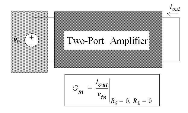
27 Finding the Transconductance G m
28 Common-Source Amplifier (again) How to isolate DC level?
29 DC Bias 5 V Neglect all AC signals 2.5 V Choose I BIAS, W/L
30 Load-Line Analysis to find Q I R D = V DD V R D out I D = 5V 10k Q 1 slope = 10k I D = 0V 10k
31 Small-Signal Analysis R in =
32 Two-Port Parameters: Find R in, R out, G m Generic Transconductance Amp R s v s + v in R in G v m in Rout RL R in = G m = g R = r R m out o D
33 Two-Port CS Model Reattach source and load one-ports:
EE105 - Fall 2006 Microelectronic Devices and Circuits
 EE105 - Fall 2006 Microelectronic Devices and Circuits Prof. Jan M. Rabaey (jan@eecs) Lecture 11: Voltage and Current Sources Administrativia Lab 3 this week Please make sure to work through the pre-lab
Lecture 20 Transistor Amplifiers (II) Other Amplifier Stages
 Other Amplifier Stages") Lecture 20 Transistor Amplifiers (II) Other Amplifier Stages Outline Common drain amplifier Common gate amplifier Reading Assignment: Howe and Sodini; Chapter 8, Sections 8.78.9 6.02 Spring 2009 . Common
Lecture 20 Transistor Amplifiers (II) Other Amplifier Stages Outline Common drain amplifier Common gate amplifier Reading Assignment: Howe and Sodini; Chapter 8, Sections 8.78.9 6.02 Spring 2009 . Common
Chapter 4 Single-stage MOS amplifiers
 Chapter 4 Single-stage MOS amplifiers ELEC-H402/CH4: Single-stage MOS amplifiers 1 Single-stage MOS amplifiers NMOS as an amplifier: example of common-source circuit NMOS amplifier example Introduction
INTRODUCTION TO ELECTRONICS EHB 222E
 INTRODUCTION TO ELECTRONICS EHB 222E MOS Field Effect Transistors (MOSFETS II) MOSFETS 1/ INTRODUCTION TO ELECTRONICS 1 MOSFETS Amplifiers Cut off when v GS < V t v DS decreases starting point A, once
Lecture 20 Transistor Amplifiers (II) Other Amplifier Stages. November 17, 2005
 Other Amplifier Stages. November 17, 2005") 6.012 Microelectronic Devices and Circuits Fall 2005 Lecture 20 1 Lecture 20 Transistor Amplifiers (II) Other Amplifier Stages November 17, 2005 Contents: 1. Common source amplifier (cont.) 2. Common drain
6.012 Microelectronic Devices and Circuits Fall 2005 Lecture 20 1 Lecture 20 Transistor Amplifiers (II) Other Amplifier Stages November 17, 2005 Contents: 1. Common source amplifier (cont.) 2. Common drain
The George Washington University School of Engineering and Applied Science Department of Electrical and Computer Engineering ECE 20 - LAB
 The George Washington University School of Engineering and Applied Science Department of Electrical and Computer Engineering ECE 20 - LAB Experiment # 11 MOSFET Amplifiers testing and designing Equipment:
Chapter 15 Goals. ac-coupled Amplifiers Example of a Three-Stage Amplifier
 Chapter 15 Goals ac-coupled multistage amplifiers including voltage gain, input and output resistances, and small-signal limitations. dc-coupled multistage amplifiers. Darlington configuration and cascode
Lecture 34: Designing amplifiers, biasing, frequency response. Context
 Lecture 34: Designing amplifiers, biasing, frequency response Prof J. S. Smith Context We will figure out more of the design parameters for the amplifier we looked at in the last lecture, and then we will
ECE315 / ECE515 Lecture 8 Date:
 ECE35 / ECE55 Lecture 8 Date: 05.09.06 CS Amplifier with Constant Current Source Current Steering Circuits CS Stage Followed by CG Stage Cascode as Current Source Cascode as Amplifier ECE35 / ECE55 CS
Lecture 19 Transistor Amplifiers (I) Common Source Amplifier. November 15, 2005
 Common Source Amplifier. November 15, 2005") 6.012 Microelectronic Devices and Circuits Fall 2005 Lecture 19 1 Lecture 19 Transistor Amplifiers (I) Common Source Amplifier November 15, 2005 Contents: 1. Amplifier fundamentals 2. Common source amplifier
6.012 Microelectronic Devices and Circuits Fall 2005 Lecture 19 1 Lecture 19 Transistor Amplifiers (I) Common Source Amplifier November 15, 2005 Contents: 1. Amplifier fundamentals 2. Common source amplifier
Week 9a OUTLINE. MOSFET I D vs. V GS characteristic Circuit models for the MOSFET. Reading. resistive switch model small-signal model
 Week 9a OUTLINE MOSFET I vs. V GS characteristic Circuit models for the MOSFET resistive switch model small-signal model Reading Rabaey et al.: Chapter 3.3.2 Hambley: Chapter 12 (through 12.5); Section
Electronic Circuits for Mechatronics ELCT 609 Lecture 7: MOS-FET Amplifiers
 Electronic Circuits for Mechatronics ELCT 609 Lecture 7: MOS-FET Amplifiers Assistant Professor Office: C3.315 E-mail: eman.azab@guc.edu.eg 1 Enhancement N-MOS Modes of Operation Mode V GS I DS V DS Cutoff
Experiment 5 Single-Stage MOS Amplifiers
 Experiment 5 Single-Stage MOS Amplifiers B. Cagdaser, H. Chong, R. Lu, and R. T. Howe UC Berkeley EE 105 Fall 2005 1 Objective This is the first lab dealing with the use of transistors in amplifiers. We
Lecture 21: Voltage/Current Buffer Freq Response
 Lecture 21: Voltage/Current Buffer Freq Response Prof. Niknejad Lecture Outline Last Time: Frequency Response of Voltage Buffer Frequency Response of Current Buffer Current Mirrors Biasing Schemes Detailed
EE311: Electrical Engineering Junior Lab, Fall 2006 Experiment 4: Basic MOSFET Characteristics and Analog Circuits
 EE311: Electrical Engineering Junior Lab, Fall 2006 Experiment 4: Basic MOSFET Characteristics and Analog Circuits Objective This experiment is designed for students to get familiar with the basic properties
Digital Electronics. Assign 1 and 0 to a range of voltage (or current), with a separation that minimizes a transition region. Positive Logic.
, with a separation that minimizes a transition region. Positive Logic.") Digital Electronics Assign 1 and 0 to a range of voltage (or current), with a separation that minimizes a transition region Positive Logic Logic 1 Negative Logic Logic 0 Voltage Transition Region Transition
Digital Electronics Assign 1 and 0 to a range of voltage (or current), with a separation that minimizes a transition region Positive Logic Logic 1 Negative Logic Logic 0 Voltage Transition Region Transition
ECE 546 Lecture 12 Integrated Circuits
 ECE 546 Lecture 12 Integrated Circuits Spring 2018 Jose E. Schutt-Aine Electrical & Computer Engineering University of Illinois jesa@illinois.edu ECE 546 Jose Schutt Aine 1 Integrated Circuits IC Requirements
D n ox GS THN DS GS THN DS GS THN. D n ox GS THN DS GS THN DS GS THN
 Name: EXAM #3 Closed book, closed notes. Calculators may be used for numeric computations only. All work is to be your own - show your work for maximum partial credit. Data: Use the following data in all
EE 330 Lecture 26. Amplifier Biasing (precursor) Two-Port Amplifier Model
 Two-Port Amplifier Model") EE 330 Lecture 26 Amplifier Biasing (precursor) Two-Port Amplifier Model Exam Schedule Exam 2 Friday October 27 Exam 3 Friday November 17 Review from Last Lecture Graphical Analysis and Interpretation
EE 330 Lecture 26 Amplifier Biasing (precursor) Two-Port Amplifier Model Exam Schedule Exam 2 Friday October 27 Exam 3 Friday November 17 Review from Last Lecture Graphical Analysis and Interpretation
IFB270 Advanced Electronic Circuits
 IFB270 Advanced Electronic Circuits Chapter 9: FET amplifiers and switching circuits Prof. Manar Mohaisen Department of EEC Engineering Review of the Precedent Lecture Review of basic electronic devices
LAB 4 : FET AMPLIFIERS
 LEARNING OUTCOME: LAB 4 : FET AMPLIFIERS In this lab, students design and implement single-stage FET amplifiers and explore the frequency response of the real amplifiers. Breadboard and the Analog Discovery
ANALOG FUNDAMENTALS C. Topic 4 BASIC FET AMPLIFIER CONFIGURATIONS
 AV18-AFC ANALOG FUNDAMENTALS C Topic 4 BASIC FET AMPLIFIER CONFIGURATIONS 1 ANALOG FUNDAMENTALS C AV18-AFC Overview This topic identifies the basic FET amplifier configurations and their principles of
ECE 442 Solid State Devices & Circuits. 15. Differential Amplifiers
 ECE 442 Solid State Devices & Circuits 15. Differential Amplifiers Jose E. Schutt-Aine Electrical & Computer Engineering University of Illinois jschutt@emlab.uiuc.edu ECE 442 Jose Schutt Aine 1 Background
ECE315 / ECE515 Lecture 5 Date:
 Lecture 5 ate: 20.08.2015 MOSFET Small Signal Models, and Analysis Common Source Amplifier Introduction MOSFET Small Signal Model To determine the small-signal performance of a given MOSFET amplifier circuit,
Course Number Section. Electronics I ELEC 311 BB Examination Date Time # of pages. Final August 12, 2005 Three hours 3 Instructor
 Course Number Section Electronics ELEC 311 BB Examination Date Time # of pages Final August 12, 2005 Three hours 3 nstructor Dr. R. Raut M aterials allowed: No Yes X (Please specify) Calculators allowed:
C H A P T E R 5. Amplifier Design
 C H A P T E 5 Amplifier Design The Common-Source Amplifier v 0 = r ( g mvgs )( D 0 ) A v0 = g m r ( D 0 ) Performing the analysis directly on the circuit diagram with the MOSFET model used implicitly.
EE 230 Fall 2006 Experiment 11. Small Signal Linear Operation of Nonlinear Devices
 EE 230 Fall 2006 Experiment 11 Small Signal Linear Operation of Nonlinear Devices Purpose: The purpose of this laboratory experiment is to investigate the use of small signal concepts for designing and
Multistage Amplifiers
 Multistage Amplifiers Single-stage transistor amplifiers are inadequate for meeting most design requirements for any of the four amplifier types (voltage, current, transconductance, and transresistance.)
Lecture 27: MOSFET Circuits at DC.
 Whites, EE 30 Lecture 7 Page 1 of 8 Lecture 7: MOSFET Circuits at C. We will illustrate the C analysis of MOSFET circuits through a number of examples in this lecture. Example N7.1 (similar to text Example
ECE315 / ECE515 Lecture 9 Date:
 Lecture 9 Date: 03.09.2015 Biasing in MOS Amplifier Circuits Biasing using Single Power Supply The general form of a single-supply MOSFET amplifier biasing circuit is: We typically attempt to satisfy three
EE105 Fall 2015 Microelectronic Devices and Circuits
 EE105 Fall 2015 Microelectronic Devices and Circuits Multi-Stage Amplifiers Prof. Ming C. Wu wu@eecs.berkeley.edu 511 Sutardja Dai Hall (SDH) Terminal Gain and I/O Resistances of MOS Amplifiers Common
Field Effect Transistors
 Field Effect Transistors LECTURE NO. - 41 Field Effect Transistors www.mycsvtunotes.in JFET MOSFET CMOS Field Effect transistors - FETs First, why are we using still another transistor? BJTs had a small
Session 2 MOS Transistor for RF Circuits
 Session 2 MOS Transistor for RF Circuits Session Speaker Chandramohan P. Session Contents MOS transistor basics MOS equivalent circuit Single stage amplifiers Opamp design Session objectives To understand
Preliminary Exam, Fall 2013 Department of Electrical and Computer Engineering University of California, Irvine EECS 170B
 Preliminary Exam, Fall 2013 Department of Electrical and Computer Engineering University of California, Irvine EECS 170B Problem 1. Consider the following circuit, where a saw-tooth voltage is applied
Electronic Devices. Floyd. Chapter 9. Ninth Edition. Electronic Devices, 9th edition Thomas L. Floyd
 Electronic Devices Ninth Edition Floyd Chapter 9 The Common-Source Amplifier In a CS amplifier, the input signal is applied to the gate and the output signal is taken from the drain. The amplifier has
ECE315 / ECE515 Lecture 7 Date:
 Lecture 7 ate: 01.09.2016 CG Amplifier Examples Biasing in MOS Amplifier Circuits Common Gate (CG) Amplifier CG Amplifier- nput is applied at the Source and the output is sensed at the rain. The Gate terminal
EE105 Fall 2015 Microelectronic Devices and Circuits
 EE105 Fall 2015 Microelectronic Devices and Circuits Prof. Ming C. Wu wu@eecs.berkeley.edu 511 Sutardja Dai Hall (SDH) 11-1 Transistor Operating Mode in Amplifiers Transistors are biased in flat part of
Lecture 030 ECE4430 Review III (1/9/04) Page 030-1
 Page 030-1") Lecture 030 ECE4430 Review III (1/9/04) Page 0301 LECTURE 030 ECE 4430 REVIEW III (READING: GHLM Chaps. 3 and 4) Objective The objective of this presentation is: 1.) Identify the prerequisite material
Lecture 030 ECE4430 Review III (1/9/04) Page 0301 LECTURE 030 ECE 4430 REVIEW III (READING: GHLM Chaps. 3 and 4) Objective The objective of this presentation is: 1.) Identify the prerequisite material
Analysis and Design of Analog Integrated Circuits Lecture 8. Cascode Techniques
 Analysis and Design of Analog Integrated Circuits Lecture 8 Cascode Techniques Michael H. Perrott February 15, 2012 Copyright 2012 by Michael H. Perrott All rights reserved. Review of Large Signal Analysis
LECTURE 19 DIFFERENTIAL AMPLIFIER
 Lecture 19 Differential Amplifier (6/4/14) Page 191 LECTURE 19 DIFFERENTIAL AMPLIFIER LECTURE ORGANIZATION Outline Characterization of a differential amplifier Differential amplifier with a current mirror
Solid State Devices & Circuits. 18. Advanced Techniques
 ECE 442 Solid State Devices & Circuits 18. Advanced Techniques Jose E. Schutt-Aine Electrical l&c Computer Engineering i University of Illinois jschutt@emlab.uiuc.edu 1 Darlington Configuration - Popular
55:041 Electronic Circuits
 55:041 Electronic Circuits Mosfet Review Sections of Chapter 3 &4 A. Kruger Mosfet Review, Page-1 Basic Structure of MOS Capacitor Sect. 3.1 Width 1 10-6 m or less Thickness 50 10-9 m or less ` MOS Metal-Oxide-Semiconductor
EE5310/EE3002: Analog Circuits. on 18th Sep. 2014
 EE5310/EE3002: Analog Circuits EC201-ANALOG CIRCUITS Tutorial 3 : PROBLEM SET 3 Due shanthi@ee.iitm.ac.in on 18th Sep. 2014 Problem 1 The MOSFET in Fig. 1 has V T = 0.7 V, and μ n C ox = 500 μa/v 2. The
Cbyp. RoutCS 2N7000. Chi-CS. Cs Cbyp. CS-CC figure 1: Two stage amplifier
 Under construction: Let me know of any errors. Design tools for Two stage DC coupled CS CC amplifier Richard Cooper October 27 2016 The Two-stage amplifier will combine two amplifiers that we have already
Course Outline. 4. Chapter 5: MOS Field Effect Transistors (MOSFET) 5. Chapter 6: Bipolar Junction Transistors (BJT)
 5. Chapter 6: Bipolar Junction Transistors (BJT)") Course Outline 1. Chapter 1: Signals and Amplifiers 1 2. Chapter 3: Semiconductors 3. Chapter 4: Diodes 4. Chapter 5: MOS Field Effect Transistors (MOSFET) 5. Chapter 6: Bipolar Junction Transistors (BJT)
Course Outline 1. Chapter 1: Signals and Amplifiers 1 2. Chapter 3: Semiconductors 3. Chapter 4: Diodes 4. Chapter 5: MOS Field Effect Transistors (MOSFET) 5. Chapter 6: Bipolar Junction Transistors (BJT)
EE 140 / EE 240A ANALOG INTEGRATED CIRCUITS FALL 2015 C. Nguyen PROBLEM SET #7
 Issued: Friday, Oct. 16, 2015 PROBLEM SET #7 Due (at 8 a.m.): Monday, Oct. 26, 2015, in the EE 140/240A HW box near 125 Cory. 1. A design error has resulted in a mismatch in the circuit of Fig. PS7-1.
Lecture 040 CE and CS Output Stages (1/11/04) Page ECE Analog Integrated Circuits and Systems II P.E. Allen
 Page ECE Analog Integrated Circuits and Systems II P.E. Allen") Lecture 040 CE and CS Output Stages (1/11/04) Page 0401 LECTURE 040 COMMON SOURCE AND EMITTER OUTPUT STAGES (READING: GHLM 8498, AH 181) Objective The objective of this presentation is: Show how to design
Lecture 040 CE and CS Output Stages (1/11/04) Page 0401 LECTURE 040 COMMON SOURCE AND EMITTER OUTPUT STAGES (READING: GHLM 8498, AH 181) Objective The objective of this presentation is: Show how to design
Design and Analysis of Two-Stage Amplifier
 Design and Analysis of Two-Stage Amplifier Introduction This report discusses the design and analysis of a two stage amplifier. An FET based common source amplifier was designed.fet was preferred over
Analog Integrated Circuit Design Exercise 1
 Analog Integrated Circuit Design Exercise 1 Integrated Electronic Systems Lab Prof. Dr.-Ing. Klaus Hofmann M.Sc. Katrin Hirmer, M.Sc. Sreekesh Lakshminarayanan Status: 21.10.2015 Pre-Assignments The lecture
Figure 1: JFET common-source amplifier. A v = V ds V gs
 Chapter 7: FET Amplifiers Switching and Circuits The Common-Source Amplifier In a common-source (CS) amplifier, the input signal is applied to the gate and the output signal is taken from the drain. The
EECS3611 Analog Integrated Circuit Design. Lecture 3. Current Source and Current Mirror
 EECS3611 Analog ntegrated Circuit Design Lecture 3 Current Source and Current Mirror ntroduction Before any device can be used in any application, it has to be properly biased so that small signal AC parameters
6.976 High Speed Communication Circuits and Systems Lecture 5 High Speed, Broadband Amplifiers
 6.976 High Speed Communication Circuits and Systems Lecture 5 High Speed, Broadband Amplifiers Michael Perrott Massachusetts Institute of Technology Copyright 2003 by Michael H. Perrott Broadband Communication
Lecture 19 - Transistor Amplifiers (I) Common-Source Amplifier. April 24, 2001
 Common-Source Amplifier. April 24, 2001") 6.012 Microelectronic Devices and Circuits Spring 2001 Lecture 191 Lecture 19 Transistor Amplifiers (I) CommonSource Amplifier April 24, 2001 Contents: 1. Amplifier fundamentals 2. Commonsource amplifier
6.012 Microelectronic Devices and Circuits Spring 2001 Lecture 191 Lecture 19 Transistor Amplifiers (I) CommonSource Amplifier April 24, 2001 Contents: 1. Amplifier fundamentals 2. Commonsource amplifier
University of Pittsburgh
 University of Pittsburgh Experiment #4 Lab Report MOSFET Amplifiers and Current Mirrors Submission Date: 07/03/2018 Instructors: Dr. Ahmed Dallal Shangqian Gao Submitted By: Nick Haver & Alex Williams
Lab 6: MOSFET AMPLIFIER
 Lab 6: MOSFET AMPLIFIER NOTE: This is a "take home" lab. You are expected to do the lab on your own time (still working with your lab partner) and then submit your lab reports. Lab instructors will be
Chapter 8 Differential and Multistage Amplifiers
 1 Chapter 8 Differential and Multistage Amplifiers Operational Amplifier Circuit Components 2 1. Ch 7: Current Mirrors and Biasing 2. Ch 9: Frequency Response 3. Ch 8: Active-Loaded Differential Pair 4.
CMOS Cascode Transconductance Amplifier
 CMOS Cascode Transconductance Amplifier Basic topology. 5 V I SUP v s V G2 M 2 iout C L v OUT Device Data V Tn = 1 V V Tp = 1 V µ n C ox = 50 µa/v 2 µ p C ox = 25 µa/v 2 λ n = 0.05 V 1 λ p = 0.02 V 1 @
Week 7: Common-Collector Amplifier, MOS Field Effect Transistor
 EE 2110A Electronic Circuits Week 7: Common-Collector Amplifier, MOS Field Effect Transistor ecture 07-1 Topics to coer Common-Collector Amplifier MOS Field Effect Transistor Physical Operation and I-V
EE 330 Lecture 20. Operating Points for Amplifier Applications Amplification with Transistor Circuits Small Signal Modelling
 EE 330 Lecture 20 Operating Points for Amplifier Applications Amplification with Transistor Circuits Small Signal Modelling Review from Last Lecture Simplified Multi-Region Model Alternate equivalent model
ENEE 307 Laboratory#2 (n-mosfet, p-mosfet, and a single n-mosfet amplifier in the common source configuration)
") Revised 2/16/2007 ENEE 307 Laboratory#2 (n-mosfet, p-mosfet, and a single n-mosfet amplifier in the common source configuration) *NOTE: The text mentioned below refers to the Sedra/Smith, 5th edition.
Revised 2/16/2007 ENEE 307 Laboratory#2 (n-mosfet, p-mosfet, and a single n-mosfet amplifier in the common source configuration) *NOTE: The text mentioned below refers to the Sedra/Smith, 5th edition.
In a cascade configuration, the overall voltage and current gains are given by:
 ECE 3274 Two-Stage Amplifier Project 1. Objective The objective of this lab is to design and build a direct coupled two-stage amplifier, including a common-source gain stage and a common-collector buffer
6.002 Circuits and Electronics Final Exam Practice Set 1
 MASSACHUSETTS INSTITUTE OF TECHNOLOGY DEPARTMENT OF ELECTRICAL ENGINEERING AND COMPUTER SCIENCE 6.002 Circuits and Electronics Set 1 Problem 1 Figure 1 shows a simplified small-signal model of a certain
SAMPLE FINAL EXAMINATION FALL TERM
 ENGINEERING SCIENCES 154 ELECTRONIC DEVICES AND CIRCUITS SAMPLE FINAL EXAMINATION FALL TERM 2001-2002 NAME Some Possible Solutions a. Please answer all of the questions in the spaces provided. If you need
Amplifier Design Using an Active Load
 THE PENNSYLVANIA STATE UNIVERSITY EE 310 : ELECTRONIC CIRCUIT DESIGN I Amplifier Design Using an Active Load William David Stranburg 1 Introduction: In Part 1 of this lab, we used an NMOS amplifying transistor
The Miller Approximation. CE Frequency Response. The exact analysis is worked out on pp of H&S.
 CE Frequency Response The exact analysis is worked out on pp. 639-64 of H&S. The Miller Approximation Therefore, we consider the effect of C µ on the input node only V ---------- out V s = r g π m ------------------
Building Blocks of Integrated-Circuit Amplifiers
 Building Blocks of ntegrated-circuit Amplifiers 1 The Basic Gain Cell CS and CE Amplifiers with Current Source Loads Current-source- or active-loaded CS amplifier Rin A o R A o g r r o g r 0 m o m o Current-source-
Lecture 20: Passive Mixers
 EECS 142 Lecture 20: Passive Mixers Prof. Ali M. Niknejad University of California, Berkeley Copyright c 2005 by Ali M. Niknejad A. M. Niknejad University of California, Berkeley EECS 142 Lecture 20 p.
MOSFET Biasing Supplement for Laboratory Experiment 5 EE348L. Spring 2005
 MOSFET Biasing Supplement for Laboratory Experiment 5 EE348L Spring 2005 B. Madhavan Spring 2005 B. Madhavan Page 1 of 10 EE348L, Spring 2005 5 Laboratory Assignment 5 biasing supplement 5.1 Biasing a
55:041 Electronic Circuits
 55:041 Electronic Circuits MOSFETs Sections of Chapter 3 &4 A. Kruger MOSFETs, Page-1 Basic Structure of MOS Capacitor Sect. 3.1 Width = 1 10-6 m or less Thickness = 50 10-9 m or less ` MOS Metal-Oxide-Semiconductor
Fundamentos de Electrónica Lab Guide
 Fundamentos de Electrónica Lab Guide Field Effect Transistor MOS-FET IST-2016/2017 2 nd Semester I-Introduction These are the objectives: a. n-type MOSFET characterization from the I(U) characteristics.
MOS Field Effect Transistors
 MOS Field Effect Transistors A gate contact gate interconnect n polysilicon gate source contacts W active area (thin oxide area) polysilicon gate contact metal interconnect drain contacts A bulk contact
Basic Electronics Prof. Dr. Chitralekha Mahanta Department of Electronics and Communication Engineering Indian Institute of Technology, Guwahati
 Basic Electronics Prof. Dr. Chitralekha Mahanta Department of Electronics and Communication Engineering Indian Institute of Technology, Guwahati Module: 3 Field Effect Transistors Lecture-8 Junction Field
Week 12: Output Stages, Frequency Response
 ELE 2110A Electronic Circuits Week 12: Output Stages, Frequency esponse (2 hours only) Lecture 12-1 Output Stages Topics to cover Amplifier Frequency esponse eading Assignment: Chap 15.3, 16.1 of Jaeger
UNIT-1 Bipolar Junction Transistors. Text Book:, Microelectronic Circuits 6 ed., by Sedra and Smith, Oxford Press
 UNIT-1 Bipolar Junction Transistors Text Book:, Microelectronic Circuits 6 ed., by Sedra and Smith, Oxford Press Figure 6.1 A simplified structure of the npn transistor. Microelectronic Circuits, Sixth
Lecture 16: MOS Transistor models: Linear models, SPICE models. Context. In the last lecture, we discussed the MOS transistor, and
 Lecture 16: MOS Transistor models: Linear models, SPICE models Context In the last lecture, we discussed the MOS transistor, and added a correction due to the changing depletion region, called the body
Electronic Circuits. Junction Field-effect Transistors. Dr. Manar Mohaisen Office: F208 Department of EECE
 Electronic Circuits Junction Field-effect Transistors Dr. Manar Mohaisen Office: F208 Email: manar.subhi@kut.ac.kr Department of EECE Review of the Precedent Lecture Explain the Operation Class A Power
F7 Transistor Amplifiers
 Lars Ohlsson 2018-09-25 F7 Transistor Amplifiers Outline Transfer characteristics Small signal operation and models Basic configurations Common source (CS) CS/CE w/ source/ emitter degeneration resistance
Homework Assignment 12
 Homework Assignment 12 Question 1 Shown the is Bode plot of the magnitude of the gain transfer function of a constant GBP amplifier. By how much will the amplifier delay a sine wave with the following
Microelectronic Devices and Circuits- EECS105 Final Exam
 EECS105 1 of 13 Fall 2000 Microelectronic Devices and Circuits- EECS105 Final Exam Wednesday, December 13, 2000 Costas J. Spanos University of California at Berkeley College of Engineering Department of
Review Sheet for Midterm #2
 Review Sheet for Midterm #2 Brian Bircumshaw brianb@eecs.berkeley.edu 1 Miterm #1 Review See Table 1 on the following page for a list of the most important equations you should know from Midterm #1. 2
BJT Amplifier. Superposition principle (linear amplifier)
") BJT Amplifier Two types analysis DC analysis Applied DC voltage source AC analysis Time varying signal source Superposition principle (linear amplifier) The response of a linear amplifier circuit excited
BJT Amplifier Two types analysis DC analysis Applied DC voltage source AC analysis Time varying signal source Superposition principle (linear amplifier) The response of a linear amplifier circuit excited
MOSFET Terminals. The voltage applied to the GATE terminal determines whether current can flow between the SOURCE & DRAIN terminals.
 MOSFET Terminals The voltage applied to the GATE terminal determines whether current can flow between the SOURCE & DRAIN terminals. For an n-channel MOSFET, the SOURCE is biased at a lower potential (often
Depletion-mode operation ( 공핍형 ): Using an input gate voltage to effectively decrease the channel size of an FET
: Using an input gate voltage to effectively decrease the channel size of an FET") Ch. 13 MOSFET Metal-Oxide-Semiconductor Field-Effect Transistor : I D D-mode E-mode V g The gate oxide is made of dielectric SiO 2 with e = 3.9 Depletion-mode operation ( 공핍형 ): Using an input gate voltage
Ch. 13 MOSFET Metal-Oxide-Semiconductor Field-Effect Transistor : I D D-mode E-mode V g The gate oxide is made of dielectric SiO 2 with e = 3.9 Depletion-mode operation ( 공핍형 ): Using an input gate voltage
MODULE-2: Field Effect Transistors (FET)
") FORMAT-1B Definition: MODULE-2: Field Effect Transistors (FET) FET is a three terminal electronic device used for variety of applications that match with BJT. In FET, an electric field is established by
FORMAT-1B Definition: MODULE-2: Field Effect Transistors (FET) FET is a three terminal electronic device used for variety of applications that match with BJT. In FET, an electric field is established by
Operational Amplifiers
 CHAPTER 9 Operational Amplifiers Analog IC Analysis and Design 9- Chih-Cheng Hsieh Outline. General Consideration. One-Stage Op Amps / Two-Stage Op Amps 3. Gain Boosting 4. Common-Mode Feedback 5. Input
Design and Layout of Two Stage High Bandwidth Operational Amplifier
 Design and Layout of Two Stage High Bandwidth Operational Amplifier Yasir Mahmood Qureshi Abstract This paper presents the design and layout of a two stage, high speed operational amplifiers using standard
12/01/2009. Practice with past exams
 EE40 Final Exam Review Prof. Nathan Cheung 12/01/2009 Practice with past exams http://hkn.eecs.berkeley.edu/exam/list/?examcourse=ee%2040 Slide 1 Overview of Course Circuit components: R, C, L, sources
L It indicates that g m is proportional to the k, W/L ratio and ( VGS Vt However, a large V GS reduces the allowable signal swing at the drain.
 Field-Effect Transistors (FETs) 3.9 MOSFET as an Aplifier Sall-signal equivalent circuit odels Discussions about the MOSFET transconductance W Forula 1: g = k n ( VGS Vt ) L It indicates that g is proportional
2. Introduction to MOS Amplifiers: Transfer Function Biasing & Small-Signal-Model Concepts
 2. Introduction to MOS Amplifiers: Transfer Function Biasing & Small-Signal-Model Concepts Reading: Sedra & Smith Sec. 5.4 (S&S 5 th Ed: Sec. 4.4) ECE 102, Fall 2011, F. Najmabadi NMOS Transfer Function
8. Characteristics of Field Effect Transistor (MOSFET)
") 1 8. Characteristics of Field Effect Transistor (MOSFET) 8.1. Objectives The purpose of this experiment is to measure input and output characteristics of n-channel and p- channel field effect transistors
1 8. Characteristics of Field Effect Transistor (MOSFET) 8.1. Objectives The purpose of this experiment is to measure input and output characteristics of n-channel and p- channel field effect transistors
Electronic Circuits Laboratory EE462G Lab #6. Small Signal Models: The MOSFET Common Source Amplifier
 Electronic Circuits Laboratory EE462G Lab #6 Small Signal Models: The MOSFET Common Source Amplifier AC and DC Analysis Amplifier circuits have DC and AC components that can be analyzed separately. The
EE 435. Lecture 6: Current Mirrors Signal Swing
 EE 435 ecture 6: Current Mirrors Signal Swing 1 Review from last lecture: Where we are at: Basic Op Amp Design Fundamental Amplifier Design Issues Single-Stage ow Gain Op Amps Single-Stage High Gain Op
UNIVERSITY OF NORTH CAROLINA AT CHARLOTTE Department of Electrical and Computer Engineering
 UNIVERSITY OF NORTH CAROLINA AT CHARLOTTE Department of Electrical and Computer Engineering EXPERIMENT 8 MOSFET AMPLIFIER CONFIGURATIONS AND INPUT/OUTPUT IMPEDANCE OBJECTIVES The purpose of this experiment
LOW-VOLTAGE, CLASS AB AND HIGH SLEW-RATE TWO STAGE OPERATIONAL AMPLIFIERS. CARLOS FERNANDO NIEVA-LOZANO, B.Sc.E.E
 LOW-VOLTAGE, CLASS AB AND HIGH SLEW-RATE TWO STAGE OPERATIONAL AMPLIFIERS BY CARLOS FERNANDO NIEVA-LOZANO, B.Sc.E.E A thesis submitted to the Graduate School in partial fulfillment of the requirements
Lecture 13 - Digital Circuits (II) MOS Inverter Circuits. October 25, 2005
 MOS Inverter Circuits. October 25, 2005") 6.12 - Microelectronic Devices and Circuits - Fall 25 Lecture 13-1 Lecture 13 - Digital Circuits (II) MOS Inverter Circuits October 25, 25 Contents: 1. NMOS inverter with resistor pull-up (cont.) 2. NMOS
6.12 - Microelectronic Devices and Circuits - Fall 25 Lecture 13-1 Lecture 13 - Digital Circuits (II) MOS Inverter Circuits October 25, 25 Contents: 1. NMOS inverter with resistor pull-up (cont.) 2. NMOS
V o. ECE2280 Homework #1 Fall Use: ignore r o, V BE =0.7, β=100 V I = sin(20t) For DC analysis, assume that the capacitors are open
 For DC analysis, assume that the capacitors are open") ECE2280 Homework #1 Fall 2011 1. Use: ignore r o, V BE =0.7, β=100 V I = 200.001sin(20t) For DC analysis, assume that the capacitors are open (a) Solve for the DC currents: a. I B b. I E c. I C (b) Solve
ECE2280 Homework #1 Fall 2011 1. Use: ignore r o, V BE =0.7, β=100 V I = 200.001sin(20t) For DC analysis, assume that the capacitors are open (a) Solve for the DC currents: a. I B b. I E c. I C (b) Solve
ECE4902 C Lab 5 MOSFET Common Source Amplifier with Active Load Bandwidth of MOSFET Common Source Amplifier: Resistive Load / Active Load
 ECE4902 C2012 - Lab 5 MOSFET Common Source Amplifier with Active Load Bandwidth of MOSFET Common Source Amplifier: Resistive Load / Active Load PURPOSE: The primary purpose of this lab is to measure the
Lecture 18: Common Emitter Amplifier.
 Whites, EE 320 Lecture 18 Page 1 of 8 Lecture 18: Common Emitter Amplifier. We will now begin the analysis of the three basic types of linear BJT small-signal amplifiers: 1. Common emitter (CE) 2. Common
The Common Source JFET Amplifier
 The Common Source JFET Amplifier Small signal amplifiers can also be made using Field Effect Transistors or FET's for short. These devices have the advantage over bipolar transistors of having an extremely
Homework Assignment 07
 Homework Assignment 07 Question 1 (Short Takes). 2 points each unless otherwise noted. 1. A single-pole op-amp has an open-loop low-frequency gain of A = 10 5 and an open loop, 3-dB frequency of 4 Hz.