INTRODUCTION TO ELECTRONICS EHB 222E
|
|
|
- Amie Fowler
- 6 years ago
- Views:
Transcription
 MOSFETS 1/ INTRODUCTION TO")
1 INTRODUCTION TO ELECTRONICS EHB 222E MOS Field Effect Transistors (MOSFETS II) MOSFETS 1/ INTRODUCTION TO ELECTRONICS 1
2 MOSFETS Amplifiers Cut off when v GS < V t v DS decreases starting point A, once transistor turns ON Initially v DS is high -> SATURATION: highest slope As v DS drops to < v GS V t -> TRIODE AT SATURATION: Coordinates of point B: (replace v DS with v GS - V t ) -> solve for v GS 2
3 Biasing the MOSFET Saturation AC signal is superimposed on DC: Small-signal voltage gain: Bias point (this is an inverting amplifier) 3
4 Biasing the MOSFET 4
5 Exercise 1 a) At saturation (preferred mode for amplification) 5
6 Exercise 1 continued b) Maximum allowable swing: v DS = 0.4 V (found in part 1) Should be > V t (0.2V) for SAT 1.8 V Max negative swing: = 0.2V Max symmetrical swing: ± 0.2 V V DS =0.4 V Indeed, v DS can go much higher in the positive side (up till 1.8 V) 6
 when:")
 avg v DS peak v DS > mean v GS + peak v")
7 Exercise 1 continued alternative way to find input swing: MOSFET is in SAT (at negative peak) when: When v DS is maximum -> v GS is minimum (inverting amplifier) avg v DS peak v DS > mean v GS + peak v GS - V t 7
8 Locating the bias (Q) point Q1: does not have sufficient room for positive swing (too close to V DD ) Q2: does not have sufficient room for negative swing (too close to triode/sat boundary) 8
9 Small-signal operation At saturation distortion I D (DC term) AC output: minimize distortion linearly proportional to input (v gs ) For negligible distortion: (neglect last term above) MOSFET transconductance 9
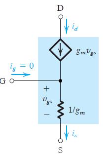
10 Small-signal operation 10
11 Small-signal Voltage gain: Small-signal assumption AC (signal) component 11
12 Small-signal Voltage gain: -> Negligible distortion at output v DSmax < V DD to avoid cut-off v DSmax > v GSmin - V t to avoid triode 12
 passes through R")
13 Small-signal equivalent models With channel-length modulation MOSFET behaves like a voltage controlled current source gm v gs current (i d ) passes through R D 13
14 Small-signal equivalent models transconductance (saturation) Isolate V OV in 2 nd equation and replace into 1st (alternative expression for g m ) Transconductance is proportional to square root of drain current Transconductance is proportional to square root of W/L Isolate k n (alternative expression for g m ) 14

15 Exercise 2 15
16 Exercise 2 continued.. First determine DC operating point -> Capacitors act as open circuit -> No current passes through R G V DS = V GS -> SATURATION For simplicity, channel-modulation is neglected for DC operating point Use V GS that is found from 1 st equation 16
17 Exercise 2 continued.. Small-signal equivalent -> capacitors are short Small-signal parameters, found using DC values (formulas drived previously) 17
18 Exercise 2 continued.. Small-signal equivalent -> capacitors are short Voltage gain Insert i i equation -> into v o Since R G is very large (10 MΩ) 18
19 Exercise 2 continued.. Small-signal equivalent -> capacitors are short 1) Input resistance 2) Input swing: transistor has to stay in SATURATION 19
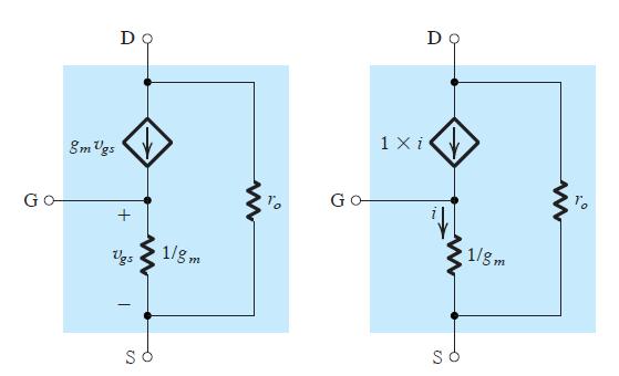
20 T-equivalent small-signal model(s) 20
 and voltage gain (A v = v o /v i")
 Common-gate amplifier!")
21 Exercise 3 Find input resistance (R in ) and voltage gain (A v = v o /v i ) Small-signal equivalent (DC current source: open) Common-gate amplifier! 21
22 MOSFET Amplifiers COMMON-SOURCE COMMON-GATE COMMON-DRAIN 22
 Neglecting channel-length modulation Overall voltage gain including")
23 Common-source amplifier (most widely used gain stage) Small-signal When v i is set to 0 Open-circuit voltage gain (v o /v i = v o /v GS ) Neglecting channel-length modulation Overall voltage gain including R L 23
 G v = A v since R in =")
24 Common-source amplifier with source resistance Resistance connected to the source T model preferred (Voltage divider) G v = A v since R in = 24
25 Common-gate amplifier (voltage divider) (same as CS, but non-inverting) 25
 (v i = 0, exclude R L )")
26 Common-drain / source follower amplifier (voltage buffer) (v i = 0, exclude R L ) 26
27 Summary & Comparison 27
28 Summary & Comparison CS configuration is best suited as the gain stage One can tune CS parameters through replacing R s CG amplifier serves well as a high frequency amplifier Source follower acts as a voltage buffer -> connects high resistance source to low resistance load -> useful as the output stage of a multistage amplifier 28
29 Biasing MOS amplifiers Fixing gate voltage (V G ) For a fixed V G -> If I D increases (for any reason) -> V GS decrases (V G is fixed) -> decreases I D (remember I D depends on V GS ) -> Therefore, R s acts as a (negative) feedback resistance, maintains I D at a constant level. PRACTICAL IMPLEMENTATIONS 29
30 Biasing MOS amplifiers Using Drain-Gate feedback resistor Large R G -> no current through R G Identical to: from previous slide -> R D serves as a (negative) feedback resistance, keeping I D constant 30
31 Biasing MOS amplifiers Constant current source Current-source implementation Drain and Gate of Q1 are connected -> SAT Q 2 shares V GS with Q1 -> Q2 assume SAT (current mirror) 31
C H A P T E R 5. Amplifier Design
 C H A P T E 5 Amplifier Design The Common-Source Amplifier v 0 = r ( g mvgs )( D 0 ) A v0 = g m r ( D 0 ) Performing the analysis directly on the circuit diagram with the MOSFET model used implicitly.
Course Outline. 4. Chapter 5: MOS Field Effect Transistors (MOSFET) 5. Chapter 6: Bipolar Junction Transistors (BJT)
 5. Chapter 6: Bipolar Junction Transistors (BJT)") Course Outline 1. Chapter 1: Signals and Amplifiers 1 2. Chapter 3: Semiconductors 3. Chapter 4: Diodes 4. Chapter 5: MOS Field Effect Transistors (MOSFET) 5. Chapter 6: Bipolar Junction Transistors (BJT)
Course Outline 1. Chapter 1: Signals and Amplifiers 1 2. Chapter 3: Semiconductors 3. Chapter 4: Diodes 4. Chapter 5: MOS Field Effect Transistors (MOSFET) 5. Chapter 6: Bipolar Junction Transistors (BJT)
ECE315 / ECE515 Lecture 9 Date:
 Lecture 9 Date: 03.09.2015 Biasing in MOS Amplifier Circuits Biasing using Single Power Supply The general form of a single-supply MOSFET amplifier biasing circuit is: We typically attempt to satisfy three
Chapter 4 Single-stage MOS amplifiers
 Chapter 4 Single-stage MOS amplifiers ELEC-H402/CH4: Single-stage MOS amplifiers 1 Single-stage MOS amplifiers NMOS as an amplifier: example of common-source circuit NMOS amplifier example Introduction
ECE315 / ECE515 Lecture 7 Date:
 Lecture 7 ate: 01.09.2016 CG Amplifier Examples Biasing in MOS Amplifier Circuits Common Gate (CG) Amplifier CG Amplifier- nput is applied at the Source and the output is sensed at the rain. The Gate terminal
Week 9a OUTLINE. MOSFET I D vs. V GS characteristic Circuit models for the MOSFET. Reading. resistive switch model small-signal model
 Week 9a OUTLINE MOSFET I vs. V GS characteristic Circuit models for the MOSFET resistive switch model small-signal model Reading Rabaey et al.: Chapter 3.3.2 Hambley: Chapter 12 (through 12.5); Section
Applied Electronics II
 Applied Electronics II Chapter 2: Differential Amplifier School of Electrical and Computer Engineering Addis Ababa Institute of Technology Addis Ababa University Daniel D./Abel G. April 4, 2016 Chapter
EE105 Fall 2015 Microelectronic Devices and Circuits
 EE105 Fall 2015 Microelectronic Devices and Circuits Prof. Ming C. Wu wu@eecs.berkeley.edu 511 Sutardja Dai Hall (SDH) 11-1 Transistor Operating Mode in Amplifiers Transistors are biased in flat part of
Electronic Circuits for Mechatronics ELCT 609 Lecture 7: MOS-FET Amplifiers
 Electronic Circuits for Mechatronics ELCT 609 Lecture 7: MOS-FET Amplifiers Assistant Professor Office: C3.315 E-mail: eman.azab@guc.edu.eg 1 Enhancement N-MOS Modes of Operation Mode V GS I DS V DS Cutoff
Lecture 20 Transistor Amplifiers (II) Other Amplifier Stages. November 17, 2005
 Other Amplifier Stages. November 17, 2005") 6.012 Microelectronic Devices and Circuits Fall 2005 Lecture 20 1 Lecture 20 Transistor Amplifiers (II) Other Amplifier Stages November 17, 2005 Contents: 1. Common source amplifier (cont.) 2. Common drain
6.012 Microelectronic Devices and Circuits Fall 2005 Lecture 20 1 Lecture 20 Transistor Amplifiers (II) Other Amplifier Stages November 17, 2005 Contents: 1. Common source amplifier (cont.) 2. Common drain
EE105 Fall 2015 Microelectronic Devices and Circuits
 EE105 Fall 2015 Microelectronic Devices and Circuits Multi-Stage Amplifiers Prof. Ming C. Wu wu@eecs.berkeley.edu 511 Sutardja Dai Hall (SDH) Terminal Gain and I/O Resistances of MOS Amplifiers Common
ECEN 474/704 Lab 6: Differential Pairs
 ECEN 474/704 Lab 6: Differential Pairs Objective Design, simulate and layout various differential pairs used in different types of differential amplifiers such as operational transconductance amplifiers
Chapter 4. CMOS Cascode Amplifiers. 4.1 Introduction. 4.2 CMOS Cascode Amplifiers
 Chapter 4 CMOS Cascode Amplifiers 4.1 Introduction A single stage CMOS amplifier cannot give desired dc voltage gain, output resistance and transconductance. The voltage gain can be made to attain higher
Lecture 20 Transistor Amplifiers (II) Other Amplifier Stages
 Other Amplifier Stages") Lecture 20 Transistor Amplifiers (II) Other Amplifier Stages Outline Common drain amplifier Common gate amplifier Reading Assignment: Howe and Sodini; Chapter 8, Sections 8.78.9 6.02 Spring 2009 . Common
Lecture 20 Transistor Amplifiers (II) Other Amplifier Stages Outline Common drain amplifier Common gate amplifier Reading Assignment: Howe and Sodini; Chapter 8, Sections 8.78.9 6.02 Spring 2009 . Common
Gechstudentszone.wordpress.com
 UNIT 4: Small Signal Analysis of Amplifiers 4.1 Basic FET Amplifiers In the last chapter, we described the operation of the FET, in particular the MOSFET, and analyzed and designed the dc response of circuits
MOSFET Amplifier Configuration. MOSFET Amplifier Configuration
 MOSFET Amplifier Configuration Single stage The signal is fed to the amplifier represented as sig with an internal resistance sig. MOSFET is represented by its small signal model. Generally interested
ECE315 / ECE515 Lecture 5 Date:
 Lecture 5 ate: 20.08.2015 MOSFET Small Signal Models, and Analysis Common Source Amplifier Introduction MOSFET Small Signal Model To determine the small-signal performance of a given MOSFET amplifier circuit,
Digital Electronics. Assign 1 and 0 to a range of voltage (or current), with a separation that minimizes a transition region. Positive Logic.
, with a separation that minimizes a transition region. Positive Logic.") Digital Electronics Assign 1 and 0 to a range of voltage (or current), with a separation that minimizes a transition region Positive Logic Logic 1 Negative Logic Logic 0 Voltage Transition Region Transition
Digital Electronics Assign 1 and 0 to a range of voltage (or current), with a separation that minimizes a transition region Positive Logic Logic 1 Negative Logic Logic 0 Voltage Transition Region Transition
ITT Technical Institute. ET215 Devices 1. Chapter
 ITT Technical Institute ET215 Devices 1 Chapter 4.6 4.7 Chapter 4 Section 4.6 FET Linear Amplifiers Transconductance of FETs The output drain current is controlled by the input signal voltage. As we earlier
Basic Electronics Prof. Dr. Chitralekha Mahanta Department of Electronics and Communication Engineering Indian Institute of Technology, Guwahati
 Basic Electronics Prof. Dr. Chitralekha Mahanta Department of Electronics and Communication Engineering Indian Institute of Technology, Guwahati Module: 3 Field Effect Transistors Lecture-3 MOSFET UNDER
F7 Transistor Amplifiers
 Lars Ohlsson 2018-09-25 F7 Transistor Amplifiers Outline Transfer characteristics Small signal operation and models Basic configurations Common source (CS) CS/CE w/ source/ emitter degeneration resistance
ANALOG FUNDAMENTALS C. Topic 4 BASIC FET AMPLIFIER CONFIGURATIONS
 AV18-AFC ANALOG FUNDAMENTALS C Topic 4 BASIC FET AMPLIFIER CONFIGURATIONS 1 ANALOG FUNDAMENTALS C AV18-AFC Overview This topic identifies the basic FET amplifier configurations and their principles of
Chapter 8 Differential and Multistage Amplifiers
 1 Chapter 8 Differential and Multistage Amplifiers Operational Amplifier Circuit Components 2 1. Ch 7: Current Mirrors and Biasing 2. Ch 9: Frequency Response 3. Ch 8: Active-Loaded Differential Pair 4.
Experiment 5 Single-Stage MOS Amplifiers
 Experiment 5 Single-Stage MOS Amplifiers B. Cagdaser, H. Chong, R. Lu, and R. T. Howe UC Berkeley EE 105 Fall 2005 1 Objective This is the first lab dealing with the use of transistors in amplifiers. We
ES 330 Electronics II Homework # 2 (Fall 2016 Due Wednesday, September 7, 2016)
") Page1 Name ES 330 Electronics II Homework # 2 (Fall 2016 Due Wednesday, September 7, 2016) Problem 1 (15 points) You are given an NMOS amplifier with drain load resistor R D = 20 k. The DC voltage (V RD
Page1 Name ES 330 Electronics II Homework # 2 (Fall 2016 Due Wednesday, September 7, 2016) Problem 1 (15 points) You are given an NMOS amplifier with drain load resistor R D = 20 k. The DC voltage (V RD
Introduction to MOSFET MOSFET (Metal Oxide Semiconductor Field Effect Transistor)
") Microelectronic Circuits Introduction to MOSFET MOSFET (Metal Oxide Semiconductor Field Effect Transistor) Slide 1 MOSFET Construction MOSFET (Metal Oxide Semiconductor Field Effect Transistor) Slide 2
Microelectronic Circuits Introduction to MOSFET MOSFET (Metal Oxide Semiconductor Field Effect Transistor) Slide 1 MOSFET Construction MOSFET (Metal Oxide Semiconductor Field Effect Transistor) Slide 2
Microelectronics Circuit Analysis and Design
 Neamen Microelectronics Chapter 4-1 Microelectronics Circuit Analysis and Design Donald A. Neamen Chapter 4 Basic FET Amplifiers Neamen Microelectronics Chapter 4-2 In this chapter, we will: Investigate
Improving Amplifier Voltage Gain
 15.1 Multistage ac-coupled Amplifiers 1077 TABLE 15.3 Three-Stage Amplifier Summary HAND ANALYSIS SPICE RESULTS Voltage gain 998 1010 Input signal range 92.7 V Input resistance 1 M 1M Output resistance
Depletion-mode operation ( 공핍형 ): Using an input gate voltage to effectively decrease the channel size of an FET
: Using an input gate voltage to effectively decrease the channel size of an FET") Ch. 13 MOSFET Metal-Oxide-Semiconductor Field-Effect Transistor : I D D-mode E-mode V g The gate oxide is made of dielectric SiO 2 with e = 3.9 Depletion-mode operation ( 공핍형 ): Using an input gate voltage
Ch. 13 MOSFET Metal-Oxide-Semiconductor Field-Effect Transistor : I D D-mode E-mode V g The gate oxide is made of dielectric SiO 2 with e = 3.9 Depletion-mode operation ( 공핍형 ): Using an input gate voltage
IENGINEERS-CONSULTANTS QUESTION BANK SERIES ELECTRONICS ENGINEERING 1 YEAR UPTU ELECTRONICS ENGINEERING EC 101 UNIT 3 (JFET AND MOSFET)
") ELECTRONICS ENGINEERING EC 101 UNIT 3 (JFET AND MOSFET) LONG QUESTIONS (10 MARKS) 1. Draw the construction diagram and explain the working of P-Channel JFET. Also draw the characteristics curve and transfer
ELECTRONICS ENGINEERING EC 101 UNIT 3 (JFET AND MOSFET) LONG QUESTIONS (10 MARKS) 1. Draw the construction diagram and explain the working of P-Channel JFET. Also draw the characteristics curve and transfer
Figure 1: JFET common-source amplifier. A v = V ds V gs
 Chapter 7: FET Amplifiers Switching and Circuits The Common-Source Amplifier In a common-source (CS) amplifier, the input signal is applied to the gate and the output signal is taken from the drain. The
Chapter 7 Building Blocks of Integrated Circuit Amplifiers: Part D: Advanced Current Mirrors
 1 Chapter 7 Building Blocks of Integrated Circuit Amplifiers: Part D: Advanced Current Mirrors Current Mirror Example 2 Two Stage Op Amp (MOSFET) Current Mirror Example Three Stage 741 Opamp (BJT) 3 4
Lecture 16: Small Signal Amplifiers
 Lecture 16: Small Signal Amplifiers Prof. Niknejad Lecture Outline Review: Small Signal Analysis Two Port Circuits Voltage Amplifiers Current Amplifiers Transconductance Amps Transresistance Amps Example:
EE5310/EE3002: Analog Circuits. on 18th Sep. 2014
 EE5310/EE3002: Analog Circuits EC201-ANALOG CIRCUITS Tutorial 3 : PROBLEM SET 3 Due shanthi@ee.iitm.ac.in on 18th Sep. 2014 Problem 1 The MOSFET in Fig. 1 has V T = 0.7 V, and μ n C ox = 500 μa/v 2. The
4.5 Biasing in MOS Amplifier Circuits
 4.5 Biasing in MOS Amplifier Circuits Biasing: establishing an appropriate DC operating point for the MOSFET - A fundamental step in the design of a MOSFET amplifier circuit An appropriate DC operating
ECEN 474/704 Lab 5: Frequency Response of Inverting Amplifiers
 ECEN 474/704 Lab 5: Frequency Response of Inverting Amplifiers Objective Design, simulate and layout various inverting amplifiers. Introduction Inverting amplifiers are fundamental building blocks of electronic
L It indicates that g m is proportional to the k, W/L ratio and ( VGS Vt However, a large V GS reduces the allowable signal swing at the drain.
 Field-Effect Transistors (FETs) 3.9 MOSFET as an Aplifier Sall-signal equivalent circuit odels Discussions about the MOSFET transconductance W Forula 1: g = k n ( VGS Vt ) L It indicates that g is proportional
Lecture 16: MOS Transistor models: Linear models, SPICE models. Context. In the last lecture, we discussed the MOS transistor, and
 Lecture 16: MOS Transistor models: Linear models, SPICE models Context In the last lecture, we discussed the MOS transistor, and added a correction due to the changing depletion region, called the body
Electronics Prof. D. C. Dube Department of Physics Indian Institute of Technology, Delhi
 Electronics Prof. D. C. Dube Department of Physics Indian Institute of Technology, Delhi Module No # 05 FETS and MOSFETS Lecture No # 06 FET/MOSFET Amplifiers and their Analysis In the previous lecture
ECE 255, MOSFET Amplifiers
 ECE 255, MOSFET Amplifiers 26 October 2017 In this lecture, the basic configurations of MOSFET amplifiers will be studied similar to that of BJT. Previously, it has been shown that with the transistor
MOSFET Common Source Amplifier
 Microelectronic Circuits MOSFET Common Source Amplifier Slide 1 Small nal Model The definition of Transconductance g m i D S S S k n W L O The definition of output resistance r o DS I The definition of
UNIT-1 Bipolar Junction Transistors. Text Book:, Microelectronic Circuits 6 ed., by Sedra and Smith, Oxford Press
 UNIT-1 Bipolar Junction Transistors Text Book:, Microelectronic Circuits 6 ed., by Sedra and Smith, Oxford Press Figure 6.1 A simplified structure of the npn transistor. Microelectronic Circuits, Sixth
SKEL 4283 Analog CMOS IC Design Current Mirrors
 SKEL 4283 Analog CMOS IC Design Current Mirrors Dr. Nasir Shaikh Husin Faculty of Electrical Engineering Universiti Teknologi Malaysia Current Mirrors 1 Objectives Introduce and characterize the current
Electronic Circuits EE359A
 Electronic Circuits EE359A Bruce McNair B206 bmcnair@stevens.edu 201-216-5549 Lecture 12 1 MOSFET vs. BJT current-voltage characteristic 1.5 10 3 i C ( v) i D ( v) 1 10 3 500 0 2 4 6 8 10 v The drain current
Field Effect Transistors
 Field Effect Transistors LECTURE NO. - 41 Field Effect Transistors www.mycsvtunotes.in JFET MOSFET CMOS Field Effect transistors - FETs First, why are we using still another transistor? BJTs had a small
IFB270 Advanced Electronic Circuits
 IFB270 Advanced Electronic Circuits Chapter 9: FET amplifiers and switching circuits Prof. Manar Mohaisen Department of EEC Engineering Review of the Precedent Lecture Review of basic electronic devices
Design and Analysis of Two-Stage Amplifier
 Design and Analysis of Two-Stage Amplifier Introduction This report discusses the design and analysis of a two stage amplifier. An FET based common source amplifier was designed.fet was preferred over
MOSFET Terminals. The voltage applied to the GATE terminal determines whether current can flow between the SOURCE & DRAIN terminals.
 MOSFET Terminals The voltage applied to the GATE terminal determines whether current can flow between the SOURCE & DRAIN terminals. For an n-channel MOSFET, the SOURCE is biased at a lower potential (often
6.976 High Speed Communication Circuits and Systems Lecture 5 High Speed, Broadband Amplifiers
 6.976 High Speed Communication Circuits and Systems Lecture 5 High Speed, Broadband Amplifiers Michael Perrott Massachusetts Institute of Technology Copyright 2003 by Michael H. Perrott Broadband Communication
Chapter 8. Field Effect Transistor
 Chapter 8. Field Effect Transistor Field Effect Transistor: The field effect transistor is a semiconductor device, which depends for its operation on the control of current by an electric field. There
Electronic Circuits for Mechatronics ELCT 609 Lecture 6: MOS-FET Transistor
 Electronic Circuits for Mechatronics ELCT 609 Lecture 6: MOS-FET Transistor Assistant Professor Office: C3.315 E-mail: eman.azab@guc.edu.eg 1 Introduction Why we call it Transistor? The name came as an
F9 Differential and Multistage Amplifiers
 Lars Ohlsson 018-10-0 F9 Differential and Multistage Amplifiers Outline MOS differential pair Common mode signal operation Differential mode signal operation Large signal operation Small signal operation
Review Sheet for Midterm #2
 Review Sheet for Midterm #2 Brian Bircumshaw brianb@eecs.berkeley.edu 1 Miterm #1 Review See Table 1 on the following page for a list of the most important equations you should know from Midterm #1. 2
Basic Electronics Prof. Dr. Chitralekha Mahanta Department of Electronics and Communication Engineering Indian Institute of Technology, Guwahati
 Basic Electronics Prof. Dr. Chitralekha Mahanta Department of Electronics and Communication Engineering Indian Institute of Technology, Guwahati Module: 3 Field Effect Transistors Lecture-8 Junction Field
D n ox GS THN DS GS THN DS GS THN. D n ox GS THN DS GS THN DS GS THN
 Name: EXAM #3 Closed book, closed notes. Calculators may be used for numeric computations only. All work is to be your own - show your work for maximum partial credit. Data: Use the following data in all
55:041 Electronic Circuits The University of Iowa Fall Exam 3. Question 1 Unless stated otherwise, each question below is 1 point.
 Exam 3 Name: Score /65 Question 1 Unless stated otherwise, each question below is 1 point. 1. An engineer designs a class-ab amplifier to deliver 2 W (sinusoidal) signal power to an resistive load. Ignoring
DC Coupling: General Trends
 DC Coupling: General Trends * Goal: want both input and output to be centered at halfway between the positive and negative supplies (or ground, for a single supply) -- in order to have maximum possible
Multistage Amplifiers
 Multistage Amplifiers Single-stage transistor amplifiers are inadequate for meeting most design requirements for any of the four amplifier types (voltage, current, transconductance, and transresistance.)
Prof. Paolo Colantonio a.a
 Prof. Paolo Colantonio a.a. 20 2 Field effect transistors (FETs) are probably the simplest form of transistor, widely used in both analogue and digital applications They are characterised by a very high
Homework Assignment 07
 Homework Assignment 07 Question 1 (Short Takes). 2 points each unless otherwise noted. 1. A single-pole op-amp has an open-loop low-frequency gain of A = 10 5 and an open loop, 3-dB frequency of 4 Hz.
The Common Source JFET Amplifier
 The Common Source JFET Amplifier Small signal amplifiers can also be made using Field Effect Transistors or FET's for short. These devices have the advantage over bipolar transistors of having an extremely
ECE 255, MOSFET Basic Configurations
 ECE 255, MOSFET Basic Configurations 8 March 2018 In this lecture, we will go back to Section 7.3, and the basic configurations of MOSFET amplifiers will be studied similar to that of BJT. Previously,
EE105 - Fall 2006 Microelectronic Devices and Circuits
 EE105 - Fall 2006 Microelectronic Devices and Circuits Prof. Jan M. Rabaey (jan@eecs) Lecture 11: Voltage and Current Sources Administrativia Lab 3 this week Please make sure to work through the pre-lab
ECE 546 Lecture 12 Integrated Circuits
 ECE 546 Lecture 12 Integrated Circuits Spring 2018 Jose E. Schutt-Aine Electrical & Computer Engineering University of Illinois jesa@illinois.edu ECE 546 Jose Schutt Aine 1 Integrated Circuits IC Requirements
Lecture 030 ECE4430 Review III (1/9/04) Page 030-1
 Page 030-1") Lecture 030 ECE4430 Review III (1/9/04) Page 0301 LECTURE 030 ECE 4430 REVIEW III (READING: GHLM Chaps. 3 and 4) Objective The objective of this presentation is: 1.) Identify the prerequisite material
Lecture 030 ECE4430 Review III (1/9/04) Page 0301 LECTURE 030 ECE 4430 REVIEW III (READING: GHLM Chaps. 3 and 4) Objective The objective of this presentation is: 1.) Identify the prerequisite material
Electronic Devices. Floyd. Chapter 9. Ninth Edition. Electronic Devices, 9th edition Thomas L. Floyd
 Electronic Devices Ninth Edition Floyd Chapter 9 The Common-Source Amplifier In a CS amplifier, the input signal is applied to the gate and the output signal is taken from the drain. The amplifier has
Phy 335, Unit 4 Transistors and transistor circuits (part one)
") Mini-lecture topics (multiple lectures): Phy 335, Unit 4 Transistors and transistor circuits (part one) p-n junctions re-visited How does a bipolar transistor works; analogy with a valve Basic circuit
Mini-lecture topics (multiple lectures): Phy 335, Unit 4 Transistors and transistor circuits (part one) p-n junctions re-visited How does a bipolar transistor works; analogy with a valve Basic circuit
Unit III FET and its Applications. 2 Marks Questions and Answers
 Unit III FET and its Applications 2 Marks Questions and Answers 1. Why do you call FET as field effect transistor? The name field effect is derived from the fact that the current is controlled by an electric
CHAPTER 8 DIFFERENTIAL AND MULTISTAGE AMPLIFIERS
 CHAPTER 8 DIFFERENTIAL AND MULTISTAGE AMPLIFIERS Chapter Outline 8.1 The CMOS Differential Pair 8. Small-Signal Operations of the MOS Differential Pair 8.3 The BJT Differential Pair 8.4 Other Non-ideal
ENEE 307 Laboratory#2 (n-mosfet, p-mosfet, and a single n-mosfet amplifier in the common source configuration)
") Revised 2/16/2007 ENEE 307 Laboratory#2 (n-mosfet, p-mosfet, and a single n-mosfet amplifier in the common source configuration) *NOTE: The text mentioned below refers to the Sedra/Smith, 5th edition.
Revised 2/16/2007 ENEE 307 Laboratory#2 (n-mosfet, p-mosfet, and a single n-mosfet amplifier in the common source configuration) *NOTE: The text mentioned below refers to the Sedra/Smith, 5th edition.
Laboratory #9 MOSFET Biasing and Current Mirror
 Laboratory #9 MOSFET Biasing and Current Mirror. Objectives 1. Review the MOSFET characteristics and transfer function. 2. Understand the relationship between the bias, the input signal and the output
Common-Source Amplifiers
 Lab 2: Common-Source Amplifiers Introduction The common-source stage is the most basic amplifier stage encountered in CMOS analog circuits. Because of its very high input impedance, moderate-to-high gain,
Chapter 8: Field Effect Transistors
 Chapter 8: Field Effect Transistors Transistors are different from the basic electronic elements in that they have three terminals. Consequently, we need more parameters to describe their behavior than
University of Pittsburgh
 University of Pittsburgh Experiment #4 Lab Report MOSFET Amplifiers and Current Mirrors Submission Date: 07/03/2018 Instructors: Dr. Ahmed Dallal Shangqian Gao Submitted By: Nick Haver & Alex Williams
BJT Amplifier. Superposition principle (linear amplifier)
") BJT Amplifier Two types analysis DC analysis Applied DC voltage source AC analysis Time varying signal source Superposition principle (linear amplifier) The response of a linear amplifier circuit excited
BJT Amplifier Two types analysis DC analysis Applied DC voltage source AC analysis Time varying signal source Superposition principle (linear amplifier) The response of a linear amplifier circuit excited
Basic Circuits. Current Mirror, Gain stage, Source Follower, Cascode, Differential Pair,
 Basic Circuits Current Mirror, Gain stage, Source Follower, Cascode, Differential Pair, CCS - Basic Circuits P. Fischer, ZITI, Uni Heidelberg, Seite 1 Reminder: Effect of Transistor Sizes Very crude classification:
Homework Assignment 07
 Homework Assignment 07 Question 1 (Short Takes). 2 points each unless otherwise noted. 1. A single-pole op-amp has an open-loop low-frequency gain of A = 10 5 and an open loop, 3-dB frequency of 4 Hz.
MOS Field Effect Transistors
 MOS Field Effect Transistors A gate contact gate interconnect n polysilicon gate source contacts W active area (thin oxide area) polysilicon gate contact metal interconnect drain contacts A bulk contact
ES 330 Electronics II Homework # 6 Soltuions (Fall 2016 Due Wednesday, October 26, 2016)
") Page1 Name Solutions ES 330 Electronics Homework # 6 Soltuions (Fall 016 ue Wednesday, October 6, 016) Problem 1 (18 points) You are given a common-emitter BJT and a common-source MOSFET (n-channel). Fill
Page1 Name Solutions ES 330 Electronics Homework # 6 Soltuions (Fall 016 ue Wednesday, October 6, 016) Problem 1 (18 points) You are given a common-emitter BJT and a common-source MOSFET (n-channel). Fill
LECTURE 19 DIFFERENTIAL AMPLIFIER
 Lecture 19 Differential Amplifier (6/4/14) Page 191 LECTURE 19 DIFFERENTIAL AMPLIFIER LECTURE ORGANIZATION Outline Characterization of a differential amplifier Differential amplifier with a current mirror
ETIN25 Analogue IC Design. Laboratory Manual Lab 2
 Department of Electrical and Information Technology LTH ETIN25 Analogue IC Design Laboratory Manual Lab 2 Jonas Lindstrand Martin Liliebladh Markus Törmänen September 2011 Laboratory 2: Design and Simulation
Chapter 5. Operational Amplifiers and Source Followers. 5.1 Operational Amplifier
 Chapter 5 Operational Amplifiers and Source Followers 5.1 Operational Amplifier In single ended operation the output is measured with respect to a fixed potential, usually ground, whereas in double-ended
Lecture 13. Biasing and Loading Single Stage FET Amplifiers. The Building Blocks of Analog Circuits - III
 Lecture 3 Biasing and Loading Single Stage FET Amplifiers The Building Blocks of Analog Circuits III In this lecture you will learn: Current biasing of circuits Current sources and sinks for CS, CG, and
Microelectronics Circuit Analysis and Design
 Microelectronics Circuit Analysis and Design Donald A. Neamen Chapter 3 The Field Effect Transistor Neamen Microelectronics, 4e Chapter 3-1 In this chapter, we will: Study and understand the operation
Microelectronics Exercises of Topic 5 ICT Systems Engineering EPSEM - UPC
 Microelectronics Exercises of Topic 5 ICT Systems Engineering EPSEM - UPC F. Xavier Moncunill Autumn 2018 5 Analog integrated circuits Exercise 5.1 This problem aims to follow the steps in the design of
Building Blocks of Integrated-Circuit Amplifiers
 CHAPTER 7 Building Blocks of Integrated-Circuit Amplifiers Introduction 7. 493 IC Design Philosophy 7. The Basic Gain Cell 494 495 7.3 The Cascode Amplifier 506 7.4 IC Biasing Current Sources, Current
EE311: Electrical Engineering Junior Lab, Fall 2006 Experiment 4: Basic MOSFET Characteristics and Analog Circuits
 EE311: Electrical Engineering Junior Lab, Fall 2006 Experiment 4: Basic MOSFET Characteristics and Analog Circuits Objective This experiment is designed for students to get familiar with the basic properties
Experiment #6 MOSFET Dynamic circuits
 Experiment #6 MOSFET Dynamic circuits Jonathan Roderick Introduction: This experiment will build upon the concepts that were presented in the previous lab and introduce dynamic circuits using MOSFETS.
MOSFET Amplifier Biasing
 MOSFET Amplifier Biasing Chris Winstead April 6, 2015 Standard Passive Biasing: Two Supplies V D V S R G I D V SS To analyze the DC behavior of this biasing circuit, it is most convenient to use the following
EE 230 Fall 2006 Experiment 11. Small Signal Linear Operation of Nonlinear Devices
 EE 230 Fall 2006 Experiment 11 Small Signal Linear Operation of Nonlinear Devices Purpose: The purpose of this laboratory experiment is to investigate the use of small signal concepts for designing and
55:041 Electronic Circuits
 55:041 Electronic Circuits Mosfet Review Sections of Chapter 3 &4 A. Kruger Mosfet Review, Page-1 Basic Structure of MOS Capacitor Sect. 3.1 Width 1 10-6 m or less Thickness 50 10-9 m or less ` MOS Metal-Oxide-Semiconductor
Difference between BJTs and FETs. Junction Field Effect Transistors (JFET)
") Difference between BJTs and FETs Transistors can be categorized according to their structure, and two of the more commonly known transistor structures, are the BJT and FET. The comparison between BJTs
Difference between BJTs and FETs Transistors can be categorized according to their structure, and two of the more commonly known transistor structures, are the BJT and FET. The comparison between BJTs
CMOS VLSI Design (A3425)
") CMOS VLSI Design (A3425) Unit V Dynamic Logic Concept Circuits Contents Charge Leakage Charge Sharing The Dynamic RAM Cell Clocks and Synchronization Clocked-CMOS Clock Generation Circuits Communication
CMOS VLSI Design (A3425) Unit V Dynamic Logic Concept Circuits Contents Charge Leakage Charge Sharing The Dynamic RAM Cell Clocks and Synchronization Clocked-CMOS Clock Generation Circuits Communication
Microelectronic Circuits. Feedback Amplifiers. Slide 1. Lecture on Microelectronics Circuits. BITS Pilani, Dubai Campus. Dr. Vilas
 Microelectronic Circuits Feedback mplifiers Slide 1 General Structure of Feedback Comparison Circuit / Mixer x o = x i ; x f = b x o ; x i = x s - x f ; f = (x o /x s ) = / (1+b). lso, x f = bx s / (1+b)
Summary. Electronics II Lecture 5(b): Metal-Oxide Si FET MOSFET. A/Lectr. Khalid Shakir Dept. Of Electrical Engineering
: Metal-Oxide Si FET MOSFET. A/Lectr. Khalid Shakir Dept. Of Electrical Engineering") Summary Electronics II Lecture 5(b): Metal-Oxide Si FET MOSFET A/Lectr. Khalid Shakir Dept. Of Electrical Engineering College of Engineering Maysan University Page 1-21 Summary The MOSFET The metal oxide
Summary Electronics II Lecture 5(b): Metal-Oxide Si FET MOSFET A/Lectr. Khalid Shakir Dept. Of Electrical Engineering College of Engineering Maysan University Page 1-21 Summary The MOSFET The metal oxide
EE 330 Lecture 20. Operating Points for Amplifier Applications Amplification with Transistor Circuits Small Signal Modelling
 EE 330 Lecture 20 Operating Points for Amplifier Applications Amplification with Transistor Circuits Small Signal Modelling Review from Last Lecture Simplified Multi-Region Model Alternate equivalent model
Low-Voltage Wide Linear Range Tunable Operational Transconductance Amplifier
 Low-Voltage Wide Linear Range Tunable Operational Transconductance Amplifier A dissertation submitted in partial fulfillment of the requirement for the award of degree of Master of Technology in VLSI Design
Operational Amplifiers
 CHAPTER 9 Operational Amplifiers Analog IC Analysis and Design 9- Chih-Cheng Hsieh Outline. General Consideration. One-Stage Op Amps / Two-Stage Op Amps 3. Gain Boosting 4. Common-Mode Feedback 5. Input
Analog Integrated Circuit Design Exercise 1
 Analog Integrated Circuit Design Exercise 1 Integrated Electronic Systems Lab Prof. Dr.-Ing. Klaus Hofmann M.Sc. Katrin Hirmer, M.Sc. Sreekesh Lakshminarayanan Status: 21.10.2015 Pre-Assignments The lecture
Chapter 13: Introduction to Switched- Capacitor Circuits
 Chapter 13: Introduction to Switched- Capacitor Circuits 13.1 General Considerations 13.2 Sampling Switches 13.3 Switched-Capacitor Amplifiers 13.4 Switched-Capacitor Integrator 13.5 Switched-Capacitor