L It indicates that g m is proportional to the k, W/L ratio and ( VGS Vt However, a large V GS reduces the allowable signal swing at the drain.
|
|
|
- Darrell Shelton
- 5 years ago
- Views:
Transcription
 L It indicates that g is proportional to the k, W/L ratio and")
1 Field-Effect Transistors (FETs) 3.9 MOSFET as an Aplifier Sall-signal equivalent circuit odels Discussions about the MOSFET transconductance W Forula 1: g = k n ( VGS Vt ) L It indicates that g is proportional to the k, W/L ratio and ( VGS Vt ) However, a large V GS reduces the allowable signal swing at the drain. Forula 2: g = 2k n W L It indicates (1) for a given MOSFET, g is proportional to the square root of the DC bias current. (2) At a given bias current, g is proportional to W / L In contrast, the transconductince of BJT is proportional to the bias current and is independent of the geoetry. I D Forula 3: g = I D ( VGS Vt ) / 2 As copared with that of BJT, for which I g = V The transconductance value for MOSFET is uch sall than that of BJT in light of the fact that the values of (V GS -V t )/2 are at least 0.1 V or so. In spite of their low g, MOSFETs have any other advantages, such as high R in, sall size, low power dissipation and ease of fabrication. C T


2 An Exaple of Sall Signals Two solutions: I D1 = A and V D = 4.4 V I D2 = A and V D < 0 which is not physically eaningful
3 An Exaple of Sall Signals The value of g is given by W g = kn ( VGS Vt ) L = 0.25( ) = A/V The output resistance VA 50 ro = = = 47kΩ I 1.06 Since R G is very large (10MW), the current through it can be neglected. v g o D v gs ( RD // RL // ro )

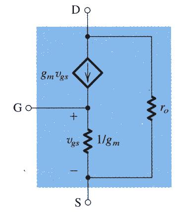
4 3.10 The T Equivalent Circuit Model
5 3.11 Biasing of MOS Aplifiers Biasing of Discrete MOSFET Aplifiers Single power suppler is used. Since I G =0, R G1 and R G2 can be very large, allowing large Rin, R S provides negative feedback. R D should be large for high gain and should be sall for large signal swing. Two power suppliers are used. Sipler bias arrangeent. R G establishes a DC ground and presents a high input resistance to a signal that ay be capacitively coupled to the gate. Even sipler and ore direct bias. A constantcurrent source I feeds the source terinal. Large resistor R G forces the V G to be equal to V D. The output signal swing should be liited in the negative direction to V t,


 A siple relation between I O and I REF")
 Current irrors")
6 3.11 Biasing of MOS Aplifiers Biasing of IC MOSFET Aplifiers Two reasons that ake the biasing circuits for discrete aplifiers not practical for IC aplifiers: (1) Extensive use of resistors; (2) Capacitively coupled input and output. Let s look at the constant current source Two significance of the constant current source: (1) A siple relation between I O and I REF by the ratio of the aspect ratios of the geoetry. When I O = I REF, it is called current irror; (2) Current irrors are essential building blocks in the design of IC aplifiers.
7 Effect of V O on I O I O will equal the I REF only at the value of V O that causes the two devices to have the sae V DS, that is V O =V GS. As V O is increased above this value, I O will increase according to the channel-length odulation. The current source and current irror have finite output resistance R O V V O A2 Ro = ro 2 I = = O IO Recall that V A is proportional to the transistor channel length; thus to obtain high output-resistance values, current sources are usually designed using transistors with long channels.


8 Current-Steering Circuits Once a constant current is generated, it can be replicated to provide DC bias currents for various aplifier stages in an IC. Current Sink Current Source
9 3.12 Basic Configurations of Single-Stage IC MOS Aplifiers Active Load Since it is difficult to ipleent resistors in ICs, people eploy current sources in place of load resistors. It is called active loaded. These diagra shows the skeletons of the three basic configurations: the coon-source (CS); the coon-gate (CG) and the coon-drain (CD) Current Source Current Sink (CS) (CG) (CD)
Lecture 34: MOSFET Common Gate Amplifier.
 Whites, EE 320 Lecture 34 Page 1 of 10 Lecture 34: MOSFET Coon Gate Aplifier. We ll continue our discussion of discrete MOSFET aplifiers we began with the coon source aplifier in Lectures 31 and 32. Here
INTRODUCTION TO ELECTRONICS EHB 222E
 INTRODUCTION TO ELECTRONICS EHB 222E MOS Field Effect Transistors (MOSFETS II) MOSFETS 1/ INTRODUCTION TO ELECTRONICS 1 MOSFETS Amplifiers Cut off when v GS < V t v DS decreases starting point A, once
ECE315 / ECE515 Lecture 9 Date:
 Lecture 9 Date: 03.09.2015 Biasing in MOS Amplifier Circuits Biasing using Single Power Supply The general form of a single-supply MOSFET amplifier biasing circuit is: We typically attempt to satisfy three
Lecture 36: MOSFET Common Drain (Source Follower) Amplifier.
 Amplifier.") Whites, EE 320 Lecture 36 Page 1 of 11 Lecture 36: MOSFET Coon Drain (Source Follower) Aplifier. The third, and last, discrete-for MOSFET aplifier we ll consider in this course is the coon drain aplifier.
Whites, EE 320 Lecture 36 Page 1 of 11 Lecture 36: MOSFET Coon Drain (Source Follower) Aplifier. The third, and last, discrete-for MOSFET aplifier we ll consider in this course is the coon drain aplifier.
ECE315 / ECE515 Lecture 7 Date:
 Lecture 7 ate: 01.09.2016 CG Amplifier Examples Biasing in MOS Amplifier Circuits Common Gate (CG) Amplifier CG Amplifier- nput is applied at the Source and the output is sensed at the rain. The Gate terminal
Figure 1: JFET common-source amplifier. A v = V ds V gs
 Chapter 7: FET Amplifiers Switching and Circuits The Common-Source Amplifier In a common-source (CS) amplifier, the input signal is applied to the gate and the output signal is taken from the drain. The
C H A P T E R 5. Amplifier Design
 C H A P T E 5 Amplifier Design The Common-Source Amplifier v 0 = r ( g mvgs )( D 0 ) A v0 = g m r ( D 0 ) Performing the analysis directly on the circuit diagram with the MOSFET model used implicitly.
Building Blocks of Integrated-Circuit Amplifiers
 Building Blocks of ntegrated-circuit Amplifiers 1 The Basic Gain Cell CS and CE Amplifiers with Current Source Loads Current-source- or active-loaded CS amplifier Rin A o R A o g r r o g r 0 m o m o Current-source-
Chapter 4 Single-stage MOS amplifiers
 Chapter 4 Single-stage MOS amplifiers ELEC-H402/CH4: Single-stage MOS amplifiers 1 Single-stage MOS amplifiers NMOS as an amplifier: example of common-source circuit NMOS amplifier example Introduction
ECE315 / ECE515 Lecture 5 Date:
 Lecture 5 ate: 20.08.2015 MOSFET Small Signal Models, and Analysis Common Source Amplifier Introduction MOSFET Small Signal Model To determine the small-signal performance of a given MOSFET amplifier circuit,
ANALOG FUNDAMENTALS C. Topic 4 BASIC FET AMPLIFIER CONFIGURATIONS
 AV18-AFC ANALOG FUNDAMENTALS C Topic 4 BASIC FET AMPLIFIER CONFIGURATIONS 1 ANALOG FUNDAMENTALS C AV18-AFC Overview This topic identifies the basic FET amplifier configurations and their principles of
A simple charge sensitive preamplifier for experiments with a small number of detector channels
 A siple charge sensitive preaplifier for experients with a sall nuber of detector channels laudio Arnaboldi and Gianluigi Pessina Istituto Nazionale di Fisica Nucleare (INFN) Università degli Studi di
ECE315 / ECE515 Lecture 8 Date:
 ECE35 / ECE55 Lecture 8 Date: 05.09.06 CS Amplifier with Constant Current Source Current Steering Circuits CS Stage Followed by CG Stage Cascode as Current Source Cascode as Amplifier ECE35 / ECE55 CS
ITT Technical Institute. ET215 Devices 1. Chapter
 ITT Technical Institute ET215 Devices 1 Chapter 4.6 4.7 Chapter 4 Section 4.6 FET Linear Amplifiers Transconductance of FETs The output drain current is controlled by the input signal voltage. As we earlier
Lecture 17. Small AC Signal Model of FET. Wednesday 6/12/2017 FET Small AC Signal Model 1-1
 Lecture 17 Sall AC Signal Model of FET Wednesday 6/12/2017 FET Sall AC Signal Model 1-1 Outline Sall AC Signal Equivalent Circuits for FETs Aplifier Circuits Exaples Introduction to Power Electronics Power
Single Stage Amplifier
 CHAPTE 3 Sle Stae Aplifier Analo IC Analysis and esin 3- Chih-Chen Hsieh Outle. Coon-Source Aplifier. Coon-Source Ap with Source eeneration 3. Coon-ra Aplifier 4. Coon-Gate Aplifier 5. Cascode Aplifier
Multistage Amplifiers
 Multistage Amplifiers Single-stage transistor amplifiers are inadequate for meeting most design requirements for any of the four amplifier types (voltage, current, transconductance, and transresistance.)
IFB270 Advanced Electronic Circuits
 IFB270 Advanced Electronic Circuits Chapter 9: FET amplifiers and switching circuits Prof. Manar Mohaisen Department of EEC Engineering Review of the Precedent Lecture Review of basic electronic devices
Chapter 7 Building Blocks of Integrated Circuit Amplifiers: Part D: Advanced Current Mirrors
 1 Chapter 7 Building Blocks of Integrated Circuit Amplifiers: Part D: Advanced Current Mirrors Current Mirror Example 2 Two Stage Op Amp (MOSFET) Current Mirror Example Three Stage 741 Opamp (BJT) 3 4
Gechstudentszone.wordpress.com
 UNIT 4: Small Signal Analysis of Amplifiers 4.1 Basic FET Amplifiers In the last chapter, we described the operation of the FET, in particular the MOSFET, and analyzed and designed the dc response of circuits
4.5 Biasing in MOS Amplifier Circuits
 4.5 Biasing in MOS Amplifier Circuits Biasing: establishing an appropriate DC operating point for the MOSFET - A fundamental step in the design of a MOSFET amplifier circuit An appropriate DC operating
Depletion-mode operation ( 공핍형 ): Using an input gate voltage to effectively decrease the channel size of an FET
: Using an input gate voltage to effectively decrease the channel size of an FET") Ch. 13 MOSFET Metal-Oxide-Semiconductor Field-Effect Transistor : I D D-mode E-mode V g The gate oxide is made of dielectric SiO 2 with e = 3.9 Depletion-mode operation ( 공핍형 ): Using an input gate voltage
Ch. 13 MOSFET Metal-Oxide-Semiconductor Field-Effect Transistor : I D D-mode E-mode V g The gate oxide is made of dielectric SiO 2 with e = 3.9 Depletion-mode operation ( 공핍형 ): Using an input gate voltage
Chapter 8 Differential and Multistage Amplifiers
 1 Chapter 8 Differential and Multistage Amplifiers Operational Amplifier Circuit Components 2 1. Ch 7: Current Mirrors and Biasing 2. Ch 9: Frequency Response 3. Ch 8: Active-Loaded Differential Pair 4.
ECE 255, MOSFET Amplifiers
 ECE 255, MOSFET Amplifiers 26 October 2017 In this lecture, the basic configurations of MOSFET amplifiers will be studied similar to that of BJT. Previously, it has been shown that with the transistor
Field-Effect Transistor (FET) is one of the two major transistors; FET derives its name from its working mechanism;
 is one of the two major transistors; FET derives its name from its working mechanism;") Chapter 3 Field-Effect Transistors (FETs) 3.1 Introduction Field-Effect Transistor (FET) is one of the two major transistors; FET derives its name from its working mechanism; The concept has been known
Chapter 3 Field-Effect Transistors (FETs) 3.1 Introduction Field-Effect Transistor (FET) is one of the two major transistors; FET derives its name from its working mechanism; The concept has been known
ECE 255, MOSFET Basic Configurations
 ECE 255, MOSFET Basic Configurations 8 March 2018 In this lecture, we will go back to Section 7.3, and the basic configurations of MOSFET amplifiers will be studied similar to that of BJT. Previously,
Laboratory #9 MOSFET Biasing and Current Mirror
 Laboratory #9 MOSFET Biasing and Current Mirror. Objectives 1. Review the MOSFET characteristics and transfer function. 2. Understand the relationship between the bias, the input signal and the output
Building Blocks of Integrated-Circuit Amplifiers
 CHAPTER 7 Building Blocks of Integrated-Circuit Amplifiers Introduction 7. 493 IC Design Philosophy 7. The Basic Gain Cell 494 495 7.3 The Cascode Amplifier 506 7.4 IC Biasing Current Sources, Current
ECE 442 Solid State Devices & Circuits. 15. Differential Amplifiers
 ECE 442 Solid State Devices & Circuits 15. Differential Amplifiers Jose E. Schutt-Aine Electrical & Computer Engineering University of Illinois jschutt@emlab.uiuc.edu ECE 442 Jose Schutt Aine 1 Background
Lecture 13. Biasing and Loading Single Stage FET Amplifiers. The Building Blocks of Analog Circuits - III
 Lecture 3 Biasing and Loading Single Stage FET Amplifiers The Building Blocks of Analog Circuits III In this lecture you will learn: Current biasing of circuits Current sources and sinks for CS, CG, and
Design and Analysis of Two-Stage Amplifier
 Design and Analysis of Two-Stage Amplifier Introduction This report discusses the design and analysis of a two stage amplifier. An FET based common source amplifier was designed.fet was preferred over
Lecture 20 Transistor Amplifiers (II) Other Amplifier Stages
 Other Amplifier Stages") Lecture 20 Transistor Amplifiers (II) Other Amplifier Stages Outline Common drain amplifier Common gate amplifier Reading Assignment: Howe and Sodini; Chapter 8, Sections 8.78.9 6.02 Spring 2009 . Common
Lecture 20 Transistor Amplifiers (II) Other Amplifier Stages Outline Common drain amplifier Common gate amplifier Reading Assignment: Howe and Sodini; Chapter 8, Sections 8.78.9 6.02 Spring 2009 . Common
Course Number Section. Electronics I ELEC 311 BB Examination Date Time # of pages. Final August 12, 2005 Three hours 3 Instructor
 Course Number Section Electronics ELEC 311 BB Examination Date Time # of pages Final August 12, 2005 Three hours 3 nstructor Dr. R. Raut M aterials allowed: No Yes X (Please specify) Calculators allowed:
Solid State Devices & Circuits. 18. Advanced Techniques
 ECE 442 Solid State Devices & Circuits 18. Advanced Techniques Jose E. Schutt-Aine Electrical l&c Computer Engineering i University of Illinois jschutt@emlab.uiuc.edu 1 Darlington Configuration - Popular
Lecture 20 Transistor Amplifiers (II) Other Amplifier Stages. November 17, 2005
 Other Amplifier Stages. November 17, 2005") 6.012 Microelectronic Devices and Circuits Fall 2005 Lecture 20 1 Lecture 20 Transistor Amplifiers (II) Other Amplifier Stages November 17, 2005 Contents: 1. Common source amplifier (cont.) 2. Common drain
6.012 Microelectronic Devices and Circuits Fall 2005 Lecture 20 1 Lecture 20 Transistor Amplifiers (II) Other Amplifier Stages November 17, 2005 Contents: 1. Common source amplifier (cont.) 2. Common drain
EE105 Fall 2015 Microelectronic Devices and Circuits
 EE105 Fall 2015 Microelectronic Devices and Circuits Multi-Stage Amplifiers Prof. Ming C. Wu wu@eecs.berkeley.edu 511 Sutardja Dai Hall (SDH) Terminal Gain and I/O Resistances of MOS Amplifiers Common
Current Mirrors. Basic BJT Current Mirror. Current mirrors are basic building blocks of analog design. Figure shows the basic NPN current mirror.
 Current Mirrors Basic BJT Current Mirror Current mirrors are basic building blocks of analog design. Figure shows the basic NPN current mirror. For its analysis, we assume identical transistors and neglect
Current Mirrors & Current steering Circuits:
 Current Mirrors & Current steering Circuits: MOS Current Steering Circuits: Once a constant current is generated, it can be replicated to provide DC bias currents for the various amplifier stages in the
Lecture 16: MOS Transistor models: Linear models, SPICE models. Context. In the last lecture, we discussed the MOS transistor, and
 Lecture 16: MOS Transistor models: Linear models, SPICE models Context In the last lecture, we discussed the MOS transistor, and added a correction due to the changing depletion region, called the body
ECE 546 Lecture 12 Integrated Circuits
 ECE 546 Lecture 12 Integrated Circuits Spring 2018 Jose E. Schutt-Aine Electrical & Computer Engineering University of Illinois jesa@illinois.edu ECE 546 Jose Schutt Aine 1 Integrated Circuits IC Requirements
F7 Transistor Amplifiers
 Lars Ohlsson 2018-09-25 F7 Transistor Amplifiers Outline Transfer characteristics Small signal operation and models Basic configurations Common source (CS) CS/CE w/ source/ emitter degeneration resistance
Electronics Prof. D. C. Dube Department of Physics Indian Institute of Technology, Delhi
 Electronics Prof. D. C. Dube Department of Physics Indian Institute of Technology, Delhi Module No # 05 FETS and MOSFETS Lecture No # 06 FET/MOSFET Amplifiers and their Analysis In the previous lecture
UNIT-1 Bipolar Junction Transistors. Text Book:, Microelectronic Circuits 6 ed., by Sedra and Smith, Oxford Press
 UNIT-1 Bipolar Junction Transistors Text Book:, Microelectronic Circuits 6 ed., by Sedra and Smith, Oxford Press Figure 6.1 A simplified structure of the npn transistor. Microelectronic Circuits, Sixth
DC Coupling: General Trends
 DC Coupling: General Trends * Goal: want both input and output to be centered at halfway between the positive and negative supplies (or ground, for a single supply) -- in order to have maximum possible
Field Effect Transistors
 Field Effect Transistors LECTURE NO. - 41 Field Effect Transistors www.mycsvtunotes.in JFET MOSFET CMOS Field Effect transistors - FETs First, why are we using still another transistor? BJTs had a small
The Common Source JFET Amplifier
 The Common Source JFET Amplifier Small signal amplifiers can also be made using Field Effect Transistors or FET's for short. These devices have the advantage over bipolar transistors of having an extremely
Course Outline. 4. Chapter 5: MOS Field Effect Transistors (MOSFET) 5. Chapter 6: Bipolar Junction Transistors (BJT)
 5. Chapter 6: Bipolar Junction Transistors (BJT)") Course Outline 1. Chapter 1: Signals and Amplifiers 1 2. Chapter 3: Semiconductors 3. Chapter 4: Diodes 4. Chapter 5: MOS Field Effect Transistors (MOSFET) 5. Chapter 6: Bipolar Junction Transistors (BJT)
Course Outline 1. Chapter 1: Signals and Amplifiers 1 2. Chapter 3: Semiconductors 3. Chapter 4: Diodes 4. Chapter 5: MOS Field Effect Transistors (MOSFET) 5. Chapter 6: Bipolar Junction Transistors (BJT)
Electronic Devices. Floyd. Chapter 9. Ninth Edition. Electronic Devices, 9th edition Thomas L. Floyd
 Electronic Devices Ninth Edition Floyd Chapter 9 The Common-Source Amplifier In a CS amplifier, the input signal is applied to the gate and the output signal is taken from the drain. The amplifier has
UNIT I BIASING OF DISCRETE BJT AND MOSFET PART A
 UNIT I BIASING OF DISCRETE BJT AND MOSFET PART A 1. Why do we choose Q point at the center of the load line? 2. Name the two techniques used in the stability of the q point.explain. 3. Give the expression
CS and CE amplifiers with loads:
 CS and CE amplifiers with loads: The Common-Source Circuit The most basic IC MOS amplifier is shown in fig.(1). The source of MOS transistor is grounded, also the drain resistor RD replaced by a constant-current
IENGINEERS-CONSULTANTS QUESTION BANK SERIES ELECTRONICS ENGINEERING 1 YEAR UPTU ELECTRONICS ENGINEERING EC 101 UNIT 3 (JFET AND MOSFET)
") ELECTRONICS ENGINEERING EC 101 UNIT 3 (JFET AND MOSFET) LONG QUESTIONS (10 MARKS) 1. Draw the construction diagram and explain the working of P-Channel JFET. Also draw the characteristics curve and transfer
ELECTRONICS ENGINEERING EC 101 UNIT 3 (JFET AND MOSFET) LONG QUESTIONS (10 MARKS) 1. Draw the construction diagram and explain the working of P-Channel JFET. Also draw the characteristics curve and transfer
EE105 Fall 2015 Microelectronic Devices and Circuits
 EE105 Fall 2015 Microelectronic Devices and Circuits Prof. Ming C. Wu wu@eecs.berkeley.edu 511 Sutardja Dai Hall (SDH) 11-1 Transistor Operating Mode in Amplifiers Transistors are biased in flat part of
Differential Amplifier with Active Load
 EEEB73 Electronics nalysis & Desin (7) Differential plifier with ctive Loa Learnin Outcoe ble to: Describe active loas. Desin a iff-ap with an active loa to yiel a specifie ifferential-oe voltae ain. Reference:
] (1) Problem 1. University of California, Berkeley Fall 2010 EE142, Problem Set #9 Solutions Prof. Jan Rabaey
![] (1) Problem 1. University of California, Berkeley Fall 2010 EE142, Problem Set #9 Solutions Prof. Jan Rabaey](/thumbs/81/84143587.jpg "] (1) Problem 1. University of California, Berkeley Fall 2010 EE142, Problem Set #9 Solutions Prof. Jan Rabaey") University of California, Berkeley Fall 00 EE4, Proble Set #9 Solutions Ain Arbabian Prof. Jan Rabaey Proble Since the ixer is a down-conversion type with low side injection f LO 700 MHz and f RF f IF
University of California, Berkeley Fall 00 EE4, Proble Set #9 Solutions Ain Arbabian Prof. Jan Rabaey Proble Since the ixer is a down-conversion type with low side injection f LO 700 MHz and f RF f IF
Lecture 16: Small Signal Amplifiers
 Lecture 16: Small Signal Amplifiers Prof. Niknejad Lecture Outline Review: Small Signal Analysis Two Port Circuits Voltage Amplifiers Current Amplifiers Transconductance Amps Transresistance Amps Example:
BJT Amplifier. Superposition principle (linear amplifier)
") BJT Amplifier Two types analysis DC analysis Applied DC voltage source AC analysis Time varying signal source Superposition principle (linear amplifier) The response of a linear amplifier circuit excited
BJT Amplifier Two types analysis DC analysis Applied DC voltage source AC analysis Time varying signal source Superposition principle (linear amplifier) The response of a linear amplifier circuit excited
EECS3611 Analog Integrated Circuit Design. Lecture 3. Current Source and Current Mirror
 EECS3611 Analog ntegrated Circuit Design Lecture 3 Current Source and Current Mirror ntroduction Before any device can be used in any application, it has to be properly biased so that small signal AC parameters
COLLECTOR DRAIN BASE GATE EMITTER. Applying a voltage to the Gate connection allows current to flow between the Drain and Source connections.
 MOSFETS Although the base current in a transistor is usually small (< 0.1 ma), some input devices (e.g. a crystal microphone) may be limited in their output. In order to overcome this, a Field Effect Transistor
EE5310/EE3002: Analog Circuits. on 18th Sep. 2014
 EE5310/EE3002: Analog Circuits EC201-ANALOG CIRCUITS Tutorial 3 : PROBLEM SET 3 Due shanthi@ee.iitm.ac.in on 18th Sep. 2014 Problem 1 The MOSFET in Fig. 1 has V T = 0.7 V, and μ n C ox = 500 μa/v 2. The
Introduction to MOSFET MOSFET (Metal Oxide Semiconductor Field Effect Transistor)
") Microelectronic Circuits Introduction to MOSFET MOSFET (Metal Oxide Semiconductor Field Effect Transistor) Slide 1 MOSFET Construction MOSFET (Metal Oxide Semiconductor Field Effect Transistor) Slide 2
Microelectronic Circuits Introduction to MOSFET MOSFET (Metal Oxide Semiconductor Field Effect Transistor) Slide 1 MOSFET Construction MOSFET (Metal Oxide Semiconductor Field Effect Transistor) Slide 2
Lecture 34: Designing amplifiers, biasing, frequency response. Context
 Lecture 34: Designing amplifiers, biasing, frequency response Prof J. S. Smith Context We will figure out more of the design parameters for the amplifier we looked at in the last lecture, and then we will
UNIVERSITY OF NORTH CAROLINA AT CHARLOTTE Department of Electrical and Computer Engineering
 UNIVERSITY OF NORTH CAROLINA AT CHARLOTTE Department of Electrical and Computer Engineering EXPERIMENT 8 MOSFET AMPLIFIER CONFIGURATIONS AND INPUT/OUTPUT IMPEDANCE OBJECTIVES The purpose of this experiment
Unit III FET and its Applications. 2 Marks Questions and Answers
 Unit III FET and its Applications 2 Marks Questions and Answers 1. Why do you call FET as field effect transistor? The name field effect is derived from the fact that the current is controlled by an electric
Experiment 5 Single-Stage MOS Amplifiers
 Experiment 5 Single-Stage MOS Amplifiers B. Cagdaser, H. Chong, R. Lu, and R. T. Howe UC Berkeley EE 105 Fall 2005 1 Objective This is the first lab dealing with the use of transistors in amplifiers. We
MOSFET Amplifier Configuration. MOSFET Amplifier Configuration
 MOSFET Amplifier Configuration Single stage The signal is fed to the amplifier represented as sig with an internal resistance sig. MOSFET is represented by its small signal model. Generally interested
ITT Technical Institute. ET215 Devices 1. Unit 7 Chapter 4, Sections
 ITT Technical Institute ET215 Devices 1 Unit 7 Chapter 4, Sections 4.1 4.3 Chapter 4 Section 4.1 Structure of Field-Effect Transistors Recall that the BJT is a current-controlling device; the field-effect
Lab 5: Differential Amplifier.
 epartent of Electrical and oputer Engineering Fall 1 Lab 5: ifferential plifier. 1. OBJETIVES Explore the operation of differential FET aplifier with resistive and active loads: Measure the coon and differential
Amplifiers and Feedback
 6 A Textbook of Operational Transconductance Aplifier and AIC Chapter Aplifiers and Feedback. INTRODUCTION Practically all circuits using Operational Transconductance Aplifiers are based around one of
Week 9a OUTLINE. MOSFET I D vs. V GS characteristic Circuit models for the MOSFET. Reading. resistive switch model small-signal model
 Week 9a OUTLINE MOSFET I vs. V GS characteristic Circuit models for the MOSFET resistive switch model small-signal model Reading Rabaey et al.: Chapter 3.3.2 Hambley: Chapter 12 (through 12.5); Section
CHAPTER 4 ULTRA WIDE BAND LOW NOISE AMPLIFIER DESIGN
 93 CHAPTER 4 ULTRA WIDE BAND LOW NOISE AMPLIFIER DESIGN 4.1 INTRODUCTION Ultra Wide Band (UWB) system is capable of transmitting data over a wide spectrum of frequency bands with low power and high data
Summary. Electronics II Lecture 5(b): Metal-Oxide Si FET MOSFET. A/Lectr. Khalid Shakir Dept. Of Electrical Engineering
: Metal-Oxide Si FET MOSFET. A/Lectr. Khalid Shakir Dept. Of Electrical Engineering") Summary Electronics II Lecture 5(b): Metal-Oxide Si FET MOSFET A/Lectr. Khalid Shakir Dept. Of Electrical Engineering College of Engineering Maysan University Page 1-21 Summary The MOSFET The metal oxide
Summary Electronics II Lecture 5(b): Metal-Oxide Si FET MOSFET A/Lectr. Khalid Shakir Dept. Of Electrical Engineering College of Engineering Maysan University Page 1-21 Summary The MOSFET The metal oxide
CHAPTER 8 DIFFERENTIAL AND MULTISTAGE AMPLIFIERS
 CHAPTER 8 DIFFERENTIAL AND MULTISTAGE AMPLIFIERS Chapter Outline 8.1 The CMOS Differential Pair 8. Small-Signal Operations of the MOS Differential Pair 8.3 The BJT Differential Pair 8.4 Other Non-ideal
Metal Oxide Semiconductor Field-Effect Transistors (MOSFETs)
") Metal Oxide Semiconductor Field-Effect Transistors (MOSFETs) Device Structure N-Channel MOSFET Providing electrons Pulling electrons (makes current flow) + + + Apply positive voltage to gate: Drives away
Metal Oxide Semiconductor Field-Effect Transistors (MOSFETs) Device Structure N-Channel MOSFET Providing electrons Pulling electrons (makes current flow) + + + Apply positive voltage to gate: Drives away
University of Pittsburgh
 University of Pittsburgh Experiment #4 Lab Report MOSFET Amplifiers and Current Mirrors Submission Date: 07/03/2018 Instructors: Dr. Ahmed Dallal Shangqian Gao Submitted By: Nick Haver & Alex Williams
MEASUREMENT AND INSTRUMENTATION STUDY NOTES UNIT-I
 MEASUREMENT AND INSTRUMENTATION STUDY NOTES The MOSFET The MOSFET Metal Oxide FET UNIT-I As well as the Junction Field Effect Transistor (JFET), there is another type of Field Effect Transistor available
SKEL 4283 Analog CMOS IC Design Current Mirrors
 SKEL 4283 Analog CMOS IC Design Current Mirrors Dr. Nasir Shaikh Husin Faculty of Electrical Engineering Universiti Teknologi Malaysia Current Mirrors 1 Objectives Introduce and characterize the current
Field-Effect Transistor
 Philadelphia University Faculty of Engineering Communication and Electronics Engineering Field-Effect Transistor Introduction FETs (Field-Effect Transistors) are much like BJTs (Bipolar Junction Transistors).
EE105 Fall 2015 Microelectronic Devices and Circuits. Basic Single-Transistor Amplifier Configurations
 EE05 Fall 205 Microelectronic Devices and Circuits Prof. Ming C. Wu wu@eecs.berkeley.edu 5 Sutardja Dai Hall (SDH 2- MOSFET Basic Single-Transistor Amplifier Configurations BJT 2-2 Two-Port Model of Amplifiers
Basic Electronics Prof. Dr. Chitralekha Mahanta Department of Electronics and Communication Engineering Indian Institute of Technology, Guwahati
 Basic Electronics Prof. Dr. Chitralekha Mahanta Department of Electronics and Communication Engineering Indian Institute of Technology, Guwahati Module: 3 Field Effect Transistors Lecture-8 Junction Field
Microelectronics Circuit Analysis and Design
 Neamen Microelectronics Chapter 4-1 Microelectronics Circuit Analysis and Design Donald A. Neamen Chapter 4 Basic FET Amplifiers Neamen Microelectronics Chapter 4-2 In this chapter, we will: Investigate
Applied Electronics II
 Applied Electronics II Chapter 2: Differential Amplifier School of Electrical and Computer Engineering Addis Ababa Institute of Technology Addis Ababa University Daniel D./Abel G. April 4, 2016 Chapter
Lecture 21: Voltage/Current Buffer Freq Response
 Lecture 21: Voltage/Current Buffer Freq Response Prof. Niknejad Lecture Outline Last Time: Frequency Response of Voltage Buffer Frequency Response of Current Buffer Current Mirrors Biasing Schemes Detailed
Advanced Operational Amplifiers
 IsLab Analog Integrated Circuit Design OPA2-47 Advanced Operational Amplifiers כ Kyungpook National University IsLab Analog Integrated Circuit Design OPA2-1 Advanced Current Mirrors and Opamps Two-stage
ES 330 Electronics II Homework # 6 Soltuions (Fall 2016 Due Wednesday, October 26, 2016)
") Page1 Name Solutions ES 330 Electronics Homework # 6 Soltuions (Fall 016 ue Wednesday, October 6, 016) Problem 1 (18 points) You are given a common-emitter BJT and a common-source MOSFET (n-channel). Fill
Page1 Name Solutions ES 330 Electronics Homework # 6 Soltuions (Fall 016 ue Wednesday, October 6, 016) Problem 1 (18 points) You are given a common-emitter BJT and a common-source MOSFET (n-channel). Fill
ES 330 Electronics II Homework # 2 (Fall 2016 Due Wednesday, September 7, 2016)
") Page1 Name ES 330 Electronics II Homework # 2 (Fall 2016 Due Wednesday, September 7, 2016) Problem 1 (15 points) You are given an NMOS amplifier with drain load resistor R D = 20 k. The DC voltage (V RD
Page1 Name ES 330 Electronics II Homework # 2 (Fall 2016 Due Wednesday, September 7, 2016) Problem 1 (15 points) You are given an NMOS amplifier with drain load resistor R D = 20 k. The DC voltage (V RD
Chapter 4. CMOS Cascode Amplifiers. 4.1 Introduction. 4.2 CMOS Cascode Amplifiers
 Chapter 4 CMOS Cascode Amplifiers 4.1 Introduction A single stage CMOS amplifier cannot give desired dc voltage gain, output resistance and transconductance. The voltage gain can be made to attain higher
Exam Write down one phrase/sentence that describes the purpose of the diodes and constant current source in the amplifier below.
 Exam 3 Name: Score /94 Question 1 Short Takes 1 point each unless noted otherwise. 1. Write down one phrase/sentence that describes the purpose of the diodes and constant current source in the amplifier
Lab 2: Common Source Amplifier.
 epartet of Electrical ad Coputer Egieerig Fall 1 Lab : Coo Source plifier. 1. OBJECTIVES Study ad characterize Coo Source aplifier: Bias CS ap usig MOSFET curret irror; Measure gai of CS ap with resistive
Session 2 MOS Transistor for RF Circuits
 Session 2 MOS Transistor for RF Circuits Session Speaker Chandramohan P. Session Contents MOS transistor basics MOS equivalent circuit Single stage amplifiers Opamp design Session objectives To understand
Chapter 12 Opertational Amplifier Circuits
 1 Chapter 12 Opertational Amplifier Circuits Learning Objectives 1) The design and analysis of the two basic CMOS op-amp architectures: the two-stage circuit and the single-stage, folded cascode circuit.
A Practical Approach to Designing MOSFET Amplifiers for a Specific Gain
 Paper ID #11289 A Practical Approach to Designing MOSFET Amplifiers for a Specific Gain Prof. James E. Globig, University of Dayton Prof. Globig joined the University of Dayton in August 1998. Before becoming
ENEE 307 Laboratory#2 (n-mosfet, p-mosfet, and a single n-mosfet amplifier in the common source configuration)
") Revised 2/16/2007 ENEE 307 Laboratory#2 (n-mosfet, p-mosfet, and a single n-mosfet amplifier in the common source configuration) *NOTE: The text mentioned below refers to the Sedra/Smith, 5th edition.
Revised 2/16/2007 ENEE 307 Laboratory#2 (n-mosfet, p-mosfet, and a single n-mosfet amplifier in the common source configuration) *NOTE: The text mentioned below refers to the Sedra/Smith, 5th edition.
Lecture 030 ECE4430 Review III (1/9/04) Page 030-1
 Page 030-1") Lecture 030 ECE4430 Review III (1/9/04) Page 0301 LECTURE 030 ECE 4430 REVIEW III (READING: GHLM Chaps. 3 and 4) Objective The objective of this presentation is: 1.) Identify the prerequisite material
Lecture 030 ECE4430 Review III (1/9/04) Page 0301 LECTURE 030 ECE 4430 REVIEW III (READING: GHLM Chaps. 3 and 4) Objective The objective of this presentation is: 1.) Identify the prerequisite material
The Miller Approximation. CE Frequency Response. The exact analysis is worked out on pp of H&S.
 CE Frequency Response The exact analysis is worked out on pp. 639-64 of H&S. The Miller Approximation Therefore, we consider the effect of C µ on the input node only V ---------- out V s = r g π m ------------------
SAMPLE FINAL EXAMINATION FALL TERM
 ENGINEERING SCIENCES 154 ELECTRONIC DEVICES AND CIRCUITS SAMPLE FINAL EXAMINATION FALL TERM 2001-2002 NAME Some Possible Solutions a. Please answer all of the questions in the spaces provided. If you need
A Basis for LDO and It s Thermal Design
 A Basis for LDO and It s Thermal Design Introduction The AIC LDO family device, a 3-terminal regulator, can be easily used with all protection features that are expected in high performance voltage regulation
Metal-Oxide-Silicon (MOS) devices PMOS. n-type
 devices PMOS. n-type") Metal-Oxide-Silicon (MOS devices Principle of MOS Field Effect Transistor transistor operation Metal (poly gate on oxide between source and drain Source and drain implants of opposite type to substrate.
Metal-Oxide-Silicon (MOS devices Principle of MOS Field Effect Transistor transistor operation Metal (poly gate on oxide between source and drain Source and drain implants of opposite type to substrate.
Chapter 5. Operational Amplifiers and Source Followers. 5.1 Operational Amplifier
 Chapter 5 Operational Amplifiers and Source Followers 5.1 Operational Amplifier In single ended operation the output is measured with respect to a fixed potential, usually ground, whereas in double-ended
EE311: Electrical Engineering Junior Lab, Fall 2006 Experiment 4: Basic MOSFET Characteristics and Analog Circuits
 EE311: Electrical Engineering Junior Lab, Fall 2006 Experiment 4: Basic MOSFET Characteristics and Analog Circuits Objective This experiment is designed for students to get familiar with the basic properties
Lecture 14. FET Current and Voltage Sources and Current Mirrors. The Building Blocks of Analog Circuits - IV
 Lecture 4 FET Current and oltage s and Current Mirrors The Building Blocks of Analog Circuits n this lecture you will learn: Current and voltage sources using FETs FET current mirrors Cascode current mirror