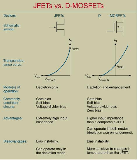
Depletion-mode operation ( 공핍형 ): Using an input gate voltage to effectively decrease the channel size of an FET
|
|
|
- Melina Owens
- 6 years ago
- Views:
Transcription
: Using an input gate voltage to effectively decrease the channel size of an FET Enhancement-mode operation ( 증가형 ): Using an input gate voltage to")
1 Ch. 13 MOSFET Metal-Oxide-Semiconductor Field-Effect Transistor : I D D-mode E-mode V g The gate oxide is made of dielectric SiO 2 with e = 3.9 Depletion-mode operation ( 공핍형 ): Using an input gate voltage to effectively decrease the channel size of an FET Enhancement-mode operation ( 증가형 ): Using an input gate voltage to effectively increase the channel size of an FET
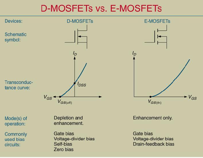
2 Basic Structure of MOSFET n-type D-MOSFET: n-type conduction channel is On at zero gate voltage with p-type substrate. For the switching operation, the channel should be depleted. It is operated in both the depletion and enhancement mode. n-type E-MOSFET: n-type conduction channel is Off at zero gate voltage with p-type substrate. For the switching operation, the channel should be enhanced. It is operated in the enhancement mode only.
3 Operation of D-MOSFET (1) Conduction channel is ON with I D = I DSS for V GS = 0 V For negative gate voltage of V GS < 0 V, the effective channel width of n-type semiconductor is reduced to decrease I D (and to increase the channel resistance) ~ depletion of electrons Thus I D < I DSS for V GS < 0 V I D I DSS V V GS 1 GS ( off ) 2
4 Operation of D-MOSFET (2) For positive gate voltage of V GS > 0 V, the effective channel width of n-type semiconductor is enlarged to increase I D (and to decrease the channel resistance) ~ accumulation of electrons and depletion of holes Thus I D > I DSS for V GS > 0 V ~ different from JFET I D I DSS V V GS 1 GS ( off ) 2
5 D-MOSFET : Drain curves & Transconductance 1 ma -6 V Drain current I D is constant for V DS > V P V P is proportional to V GS Transconductance is given by Saturated I D does not depend on V DS g m g m0 V V GS 1 GS ( off ) Since I D can be larger than I DSS, g m can be larger than g m0
6 D-MOSFET : Biasing circuits The gate voltage of V GS need not to be negative in D-MOSFET ~ different from JFET Gate-, self-, and voltage-divider-biasing is used for the operation of MOSFET Additionally, zero-biasing circuit is used for D-MOSFET ~ V GS = 0 V, I D = I DSS, R S = 0
7
8 E-MOSFET Initially, the conduction channel is OFF (I D = 0) for V GS = 0 V For positive gate voltage of V GS > 0 V, the holes in p-type substrate is depleted and the electrons are accumulated in n-type semiconductor to open the conduction channel. More positive V GS increases both the channel width and I D.
9 E-MOSFET: Transconductance Curve V GS > V GS(th) V for the Turn On state (I D 0) I k V V D GS GS ( th) k V I D( on) V GS ( on) GS ( th) 2 2 Difference with the transconductance curve in JFET: The current-on V GS is always positive Turn-on (or turn-off) point of V GS is called as a threshold voltage of V GS(th)
![[Ex. 13-2] For an E-MOSFET of #3N171, I D(on) = 10 ma, V GS = 10 V, and V GS(th) = 1.5 V are given. Find out I D for the circuit below. 10 ma 1.5 V 10 V I 10mA k 1.](/docs-images/78/78584609/images/10-0.jpg "3810 A / V V 10V 1.5V GS ( on) V GS ( th) Since R 0, V V D( on) 4 2 2 2 S GS G R 2 VG VDD 10V 5V R1R 2 2M 1M 4 2 2 2 ID k VGS V GS ( th) 1.3810 A / V 5V 1.5V 1.69mA")
10 [Ex. 13-2] For an E-MOSFET of #3N171, I D(on) = 10 ma, V GS = 10 V, and V GS(th) = 1.5 V are given. Find out I D for the circuit below. 10 ma 1.5 V 10 V I 10mA k A / V V 10V 1.5V GS ( on) V GS ( th) Since R 0, V V D( on) S GS G R 2 VG VDD 10V 5V R1R 2 2M 1M ID k VGS V GS ( th) A / V 5V 1.5V 1.69mA
 between drain and gate Since no current flows through R G, V G = V D and thus V GS = V DS V R DD D Since V DS = V DD I D R D,")
11 E-MOSFET: Drain-Feedback Bias Self-bias or zero-bias circuit is not available for an E-MOSFET due to a negative V GS Voltage-divider-, gate-, and drain-feedback-bias are used for an E-MOSFET Drain-feedback bias circuit is shown below: We put gate resistance (R G ) between drain and gate Since no current flows through R G, V G = V D and thus V GS = V DS V R DD D Since V DS = V DD I D R D, I D 0 for VGS VDD VDD VDS VDD VGS VDD R for VGS 0 D RD RD When V GS = V DS, I D = I D(on) I D ( on ) V GS V DS V DD
![[Ex. 13-3] For an E-MOSFET of #3N170 with I D(on) = 10 ma, Find out V DS and I D for the circuit below.](/docs-images/78/78584609/images/12-0.jpg "DS DD D D( on) D( on) V V R I 20V 1k 10mA 10V I I 10mA D Small-signal operation of the E-MOSFET")
12 [Ex. 13-3] For an E-MOSFET of #3N170 with I D(on) = 10 ma, Find out V DS and I D for the circuit below. DS DD D D( on) D( on) V V R I 20V 1k 10mA 10V I I 10mA D Small-signal operation of the E-MOSFET amplifier
13


14 Dual-Gate MOSFET MOSFET as a large capacitor ~ High-frequency application is limited Two gate electrodes for a MOSFET ~ total capacitance of two capacitors in series is smaller than the respective capacitance Reduced capacitance of a MOSFET using dual-gate electrodes
15 Complementary MOSFET (CMOS) Digital signal consists of rapidly-switching dc voltage levels Logic levels ~ dc 0 V and +5 V Logic families: Groups of digital circuits with nearly identical characteristics CMOS: A logic families of MOSFETs
16 CMOS Inverter Digital circuit that converts one logic level to another Example: Input = 0 V Output = 5 V Input = 5 V Output = 0 V p-channel E-MOSFET n-channel E-MOSFET
17 CMOS Inverter: p-channel E-MOSFET I D V GS At V GS = 0, the drain current is turned off ~ I D = 0 When V GS = -5 V, the p-channel is turned on Note that V SS = +5 V and V input = 0 V or +5 V V GS = V in - V SS V in V SS V GS Q 1 +5 V +5 V 0 V OFF 0 V + 5 V -5 V ON
18 CMOS Inverter: n-channel E-MOSFET I D V GS At V GS = 0, the drain current is turned off ~ I D = 0 When V GS = +5 V, the n-channel is turned on Note that V DD = +5 V and V input = 0 V or +5 V Since the source is grounded, V GS = V in V in V GS Q 2 +5 V +5 V ON 0 V 0 V OFF
 Q 1 Q 2 V out (V) 0 On Off +5 +5")
19 CMOS Inverter Q 2 as a drain resistance of Q 1 Q 1 as a drain resistance of Q 2 Q1 Q2 V in (V) Q 1 Q 2 V out (V) 0 On Off Off On 0
20 CMOS NAND gate A B AND NAND T T T F T F F T F T F T F F F T V A V B V out 5 V 5 V 0 V 5 V 0 V 5 V 0 V 5 V 5 V 0 V 0 V 5 V V SS = +5 V Input Switching Q 1 Q 2 V out V A = 5 V V A = 0 V V B = 5 V Q 2 off, Q 3 on Q 2 on, Q 3 off Q 1 off, Q 4 on V A Q 3 V B = 0 V Q 1 on, Q 4 off V B Q 4 Q1, Q2 Q3, Q4
21 CMOS fabrication
22 HW Ch.13 Due = 11/15 (Friday) 15:00 #1. Problem 13-1 #2. Problem 13-5 #3. Problem #4. Problem 13-22
Field-Effect Transistor (FET) is one of the two major transistors; FET derives its name from its working mechanism;
 is one of the two major transistors; FET derives its name from its working mechanism;") Chapter 3 Field-Effect Transistors (FETs) 3.1 Introduction Field-Effect Transistor (FET) is one of the two major transistors; FET derives its name from its working mechanism; The concept has been known
Chapter 3 Field-Effect Transistors (FETs) 3.1 Introduction Field-Effect Transistor (FET) is one of the two major transistors; FET derives its name from its working mechanism; The concept has been known
FET. FET (field-effect transistor) JFET. Prepared by Engr. JP Timola Reference: Electronic Devices by Floyd
 JFET. Prepared by Engr. JP Timola Reference: Electronic Devices by Floyd") FET Prepared by Engr. JP Timola Reference: Electronic Devices by Floyd FET (field-effect transistor) unipolar devices - unlike BJTs that use both electron and hole current, they operate only with one type
FET Prepared by Engr. JP Timola Reference: Electronic Devices by Floyd FET (field-effect transistor) unipolar devices - unlike BJTs that use both electron and hole current, they operate only with one type
Q1. Explain the construction and principle of operation of N-Channel and P-Channel Junction Field Effect Transistor (JFET).
.") Q. Explain the construction and principle of operation of N-Channel and P-Channel Junction Field Effect Transistor (JFET). Answer: N-Channel Junction Field Effect Transistor (JFET) Construction: Drain(D)
Q. Explain the construction and principle of operation of N-Channel and P-Channel Junction Field Effect Transistor (JFET). Answer: N-Channel Junction Field Effect Transistor (JFET) Construction: Drain(D)
IFB270 Advanced Electronic Circuits
 IFB270 Advanced Electronic Circuits Chapter 9: FET amplifiers and switching circuits Prof. Manar Mohaisen Department of EEC Engineering Review of the Precedent Lecture Review of basic electronic devices
L MOSFETS, IDENTIFICATION, CURVES. PAGE 1. I. Review of JFET (DRAW symbol for n-channel type, with grounded source)
") L.107.4 MOSFETS, IDENTIFICATION, CURVES. PAGE 1 I. Review of JFET (DRAW symbol for n-channel type, with grounded source) 1. "normally on" device A. current from source to drain when V G = 0 no need to
L.107.4 MOSFETS, IDENTIFICATION, CURVES. PAGE 1 I. Review of JFET (DRAW symbol for n-channel type, with grounded source) 1. "normally on" device A. current from source to drain when V G = 0 no need to
IENGINEERS-CONSULTANTS QUESTION BANK SERIES ELECTRONICS ENGINEERING 1 YEAR UPTU ELECTRONICS ENGINEERING EC 101 UNIT 3 (JFET AND MOSFET)
") ELECTRONICS ENGINEERING EC 101 UNIT 3 (JFET AND MOSFET) LONG QUESTIONS (10 MARKS) 1. Draw the construction diagram and explain the working of P-Channel JFET. Also draw the characteristics curve and transfer
ELECTRONICS ENGINEERING EC 101 UNIT 3 (JFET AND MOSFET) LONG QUESTIONS (10 MARKS) 1. Draw the construction diagram and explain the working of P-Channel JFET. Also draw the characteristics curve and transfer
Summary. Electronics II Lecture 5(b): Metal-Oxide Si FET MOSFET. A/Lectr. Khalid Shakir Dept. Of Electrical Engineering
: Metal-Oxide Si FET MOSFET. A/Lectr. Khalid Shakir Dept. Of Electrical Engineering") Summary Electronics II Lecture 5(b): Metal-Oxide Si FET MOSFET A/Lectr. Khalid Shakir Dept. Of Electrical Engineering College of Engineering Maysan University Page 1-21 Summary The MOSFET The metal oxide
Summary Electronics II Lecture 5(b): Metal-Oxide Si FET MOSFET A/Lectr. Khalid Shakir Dept. Of Electrical Engineering College of Engineering Maysan University Page 1-21 Summary The MOSFET The metal oxide
Electronic Circuits. Junction Field-effect Transistors. Dr. Manar Mohaisen Office: F208 Department of EECE
 Electronic Circuits Junction Field-effect Transistors Dr. Manar Mohaisen Office: F208 Email: manar.subhi@kut.ac.kr Department of EECE Review of the Precedent Lecture Explain the Operation Class A Power
Introduction to MOSFET MOSFET (Metal Oxide Semiconductor Field Effect Transistor)
") Microelectronic Circuits Introduction to MOSFET MOSFET (Metal Oxide Semiconductor Field Effect Transistor) Slide 1 MOSFET Construction MOSFET (Metal Oxide Semiconductor Field Effect Transistor) Slide 2
Microelectronic Circuits Introduction to MOSFET MOSFET (Metal Oxide Semiconductor Field Effect Transistor) Slide 1 MOSFET Construction MOSFET (Metal Oxide Semiconductor Field Effect Transistor) Slide 2
Chapter 5: Field Effect Transistors
 Chapter 5: Field Effect Transistors Slide 1 FET FET s (Field Effect Transistors) are much like BJT s (Bipolar Junction Transistors). Similarities: Amplifiers Switching devices Impedance matching circuits
Field Effect Transistors
 Chapter 5: Field Effect Transistors Slide 1 FET FET s (Field Effect Transistors) are much like BJT s (Bipolar Junction Transistors). Similarities: Amplifiers Switching devices Impedance matching circuits
C H A P T E R 5. Amplifier Design
 C H A P T E 5 Amplifier Design The Common-Source Amplifier v 0 = r ( g mvgs )( D 0 ) A v0 = g m r ( D 0 ) Performing the analysis directly on the circuit diagram with the MOSFET model used implicitly.
Lecture 15. Field Effect Transistor (FET) Wednesday 29/11/2017 MOSFET 1-1
 Wednesday 29/11/2017 MOSFET 1-1") Lecture 15 Field Effect Transistor (FET) Wednesday 29/11/2017 MOSFET 1-1 Outline MOSFET transistors Introduction to MOSFET MOSFET Types epletion-type MOSFET Characteristics Comparison between JFET and
Lecture 15 Field Effect Transistor (FET) Wednesday 29/11/2017 MOSFET 1-1 Outline MOSFET transistors Introduction to MOSFET MOSFET Types epletion-type MOSFET Characteristics Comparison between JFET and
Three Terminal Devices
 Three Terminal Devices - field effect transistor (FET) - bipolar junction transistor (BJT) - foundation on which modern electronics is built - active devices - devices described completely by considering
CHAPTER 8 FIELD EFFECT TRANSISTOR (FETs)
") CHAPTER 8 FIELD EFFECT TRANSISTOR (FETs) INTRODUCTION - FETs are voltage controlled devices as opposed to BJT which are current controlled. - There are two types of FETs. o Junction FET (JFET) o Metal
CHAPTER 8 FIELD EFFECT TRANSISTOR (FETs) INTRODUCTION - FETs are voltage controlled devices as opposed to BJT which are current controlled. - There are two types of FETs. o Junction FET (JFET) o Metal
Prof. Paolo Colantonio a.a
 Prof. Paolo Colantonio a.a. 20 2 Field effect transistors (FETs) are probably the simplest form of transistor, widely used in both analogue and digital applications They are characterised by a very high
ITT Technical Institute. ET215 Devices 1. Unit 8 Chapter 4, Sections
 ITT Technical Institute ET215 Devices 1 Unit 8 Chapter 4, Sections 4.4 4.5 Chapter 4 Section 4.4 MOSFET Characteristics A Metal-Oxide semiconductor field-effect transistor is the other major category of
Field Effect Transistor (FET) FET 1-1
 FET 1-1") Field Effect Transistor (FET) FET 1-1 Outline MOSFET transistors ntroduction to MOSFET MOSFET Types epletion-type MOSFET Characteristics Biasing Circuits and Examples Comparison between JFET and epletion-type
Field Effect Transistor (FET) FET 1-1 Outline MOSFET transistors ntroduction to MOSFET MOSFET Types epletion-type MOSFET Characteristics Biasing Circuits and Examples Comparison between JFET and epletion-type
Chapter 6: Field-Effect Transistors
 Chapter 6: Field-Effect Transistors Islamic University of Gaza Dr. Talal Skaik MOSFETs MOSFETs have characteristics similar to JFETs and additional characteristics that make then very useful. There are
MEASUREMENT AND INSTRUMENTATION STUDY NOTES UNIT-I
 MEASUREMENT AND INSTRUMENTATION STUDY NOTES The MOSFET The MOSFET Metal Oxide FET UNIT-I As well as the Junction Field Effect Transistor (JFET), there is another type of Field Effect Transistor available
Analog Electronics. Electronic Devices, 9th edition Thomas L. Floyd Pearson Education. Upper Saddle River, NJ, All rights reserved.
 Analog Electronics BJT Structure The BJT has three regions called the emitter, base, and collector. Between the regions are junctions as indicated. The base is a thin lightly doped region compared to the
FET(Field Effect Transistor)
") Field Effect Transistor: Construction and Characteristic of JFETs. Transfer Characteristic. CS,CD,CG amplifier and analysis of CS amplifier MOSFET (Depletion and Enhancement) Type, Transfer Characteristic,
Field Effect Transistor: Construction and Characteristic of JFETs. Transfer Characteristic. CS,CD,CG amplifier and analysis of CS amplifier MOSFET (Depletion and Enhancement) Type, Transfer Characteristic,
MOSFET & IC Basics - GATE Problems (Part - I)
") MOSFET & IC Basics - GATE Problems (Part - I) 1. Channel current is reduced on application of a more positive voltage to the GATE of the depletion mode n channel MOSFET. (True/False) [GATE 1994: 1 Mark]
MOSFET & IC Basics - GATE Problems (Part - I) 1. Channel current is reduced on application of a more positive voltage to the GATE of the depletion mode n channel MOSFET. (True/False) [GATE 1994: 1 Mark]
Lecture 13. Metal Oxide Semiconductor Field Effect Transistor (MOSFET) MOSFET 1-1
 MOSFET 1-1") Lecture 13 Metal Oxide Semiconductor Field Effect Transistor (MOSFET) MOSFET 1-1 Outline Continue MOSFET Qualitative Operation epletion-type MOSFET Characteristics Biasing Circuits and Examples Enhancement-type
Lecture 13 Metal Oxide Semiconductor Field Effect Transistor (MOSFET) MOSFET 1-1 Outline Continue MOSFET Qualitative Operation epletion-type MOSFET Characteristics Biasing Circuits and Examples Enhancement-type
Chapter 6: Field-Effect Transistors
 Chapter 6: Field-Effect Transistors FETs vs. BJTs Similarities: Amplifiers Switching devices Impedance matching circuits Differences: FETs are voltage controlled devices. BJTs are current controlled devices.
EE70 - Intro. Electronics
 EE70 - Intro. Electronics Course website: ~/classes/ee70/fall05 Today s class agenda (November 28, 2005) review Serial/parallel resonant circuits Diode Field Effect Transistor (FET) f 0 = Qs = Qs = 1 2π
INTRODUCTION: Basic operating principle of a MOSFET:
 INTRODUCTION: Along with the Junction Field Effect Transistor (JFET), there is another type of Field Effect Transistor available whose Gate input is electrically insulated from the main current carrying
8. Characteristics of Field Effect Transistor (MOSFET)
") 1 8. Characteristics of Field Effect Transistor (MOSFET) 8.1. Objectives The purpose of this experiment is to measure input and output characteristics of n-channel and p- channel field effect transistors
1 8. Characteristics of Field Effect Transistor (MOSFET) 8.1. Objectives The purpose of this experiment is to measure input and output characteristics of n-channel and p- channel field effect transistors
MOSFET Terminals. The voltage applied to the GATE terminal determines whether current can flow between the SOURCE & DRAIN terminals.
 MOSFET Terminals The voltage applied to the GATE terminal determines whether current can flow between the SOURCE & DRAIN terminals. For an n-channel MOSFET, the SOURCE is biased at a lower potential (often
Figure 1: JFET common-source amplifier. A v = V ds V gs
 Chapter 7: FET Amplifiers Switching and Circuits The Common-Source Amplifier In a common-source (CS) amplifier, the input signal is applied to the gate and the output signal is taken from the drain. The
Field Effect Transistors (npn)
") Field Effect Transistors (npn) gate drain source FET 3 terminal device channel e - current from source to drain controlled by the electric field generated by the gate base collector emitter BJT 3 terminal
Field Effect Transistors (npn) gate drain source FET 3 terminal device channel e - current from source to drain controlled by the electric field generated by the gate base collector emitter BJT 3 terminal
Design cycle for MEMS
 Design cycle for MEMS Design cycle for ICs IC Process Selection nmos CMOS BiCMOS ECL for logic for I/O and driver circuit for critical high speed parts of the system The Real Estate of a Wafer MOS Transistor
UNIT 3: FIELD EFFECT TRANSISTORS
 FIELD EFFECT TRANSISTOR: UNIT 3: FIELD EFFECT TRANSISTORS The field effect transistor is a semiconductor device, which depends for its operation on the control of current by an electric field. There are
COLLECTOR DRAIN BASE GATE EMITTER. Applying a voltage to the Gate connection allows current to flow between the Drain and Source connections.
 MOSFETS Although the base current in a transistor is usually small (< 0.1 ma), some input devices (e.g. a crystal microphone) may be limited in their output. In order to overcome this, a Field Effect Transistor
6. Field-Effect Transistor
 6. Outline: Introduction to three types of FET: JFET MOSFET & CMOS MESFET Constructions, Characteristics & Transfer curves of: JFET & MOSFET Introduction The field-effect transistor (FET) is a threeterminal
Field Effect Transistors
 Field Effect Transistors LECTURE NO. - 41 Field Effect Transistors www.mycsvtunotes.in JFET MOSFET CMOS Field Effect transistors - FETs First, why are we using still another transistor? BJTs had a small
I E I C since I B is very small
 Figure 2: Symbols and nomenclature of a (a) npn and (b) pnp transistor. The BJT consists of three regions, emitter, base, and collector. The emitter and collector are usually of one type of doping, while
FIELD EFFECT TRANSISTOR (FET) 1. JUNCTION FIELD EFFECT TRANSISTOR (JFET)
 1. JUNCTION FIELD EFFECT TRANSISTOR (JFET)") FIELD EFFECT TRANSISTOR (FET) The field-effect transistor (FET) is a three-terminal device used for a variety of applications that match, to a large extent, those of the BJT transistor. Although there
FIELD EFFECT TRANSISTOR (FET) The field-effect transistor (FET) is a three-terminal device used for a variety of applications that match, to a large extent, those of the BJT transistor. Although there
FET. Field Effect Transistors ELEKTRONIKA KONTROL. Eka Maulana, ST, MT, M.Eng. Universitas Brawijaya. p + S n n-channel. Gate. Basic structure.
 FET Field Effect Transistors ELEKTRONIKA KONTROL Basic structure Gate G Source S n n-channel Cross section p + p + p + G Depletion region Drain D Eka Maulana, ST, MT, M.Eng. Universitas Brawijaya S Channel
ECE 340 Lecture 37 : Metal- Insulator-Semiconductor FET Class Outline:
 ECE 340 Lecture 37 : Metal- Insulator-Semiconductor FET Class Outline: Metal-Semiconductor Junctions MOSFET Basic Operation MOS Capacitor Things you should know when you leave Key Questions What is the
KOM2751 Analog Electronics :: Dr. Muharrem Mercimek :: YTU - Control and Automation Dept. 1 6 FIELD-EFFECT TRANSISTORS
 KOM2751 Analog Electronics :: Dr. Muharrem Mercimek :: YTU - Control and Automation Dept. 1 6 FIELD-EFFECT TRANSISTORS Most of the content is from the textbook: Electronic devices and circuit theory, Robert
MOS Capacitance and Introduction to MOSFETs
 ECE-305: Fall 2016 MOS Capacitance and Introduction to MOSFETs Professor Peter Bermel Electrical and Computer Engineering Purdue University, West Lafayette, IN USA pbermel@purdue.edu 11/4/2016 Pierret,
ECE520 VLSI Design. Lecture 2: Basic MOS Physics. Payman Zarkesh-Ha
 ECE520 VLSI Design Lecture 2: Basic MOS Physics Payman Zarkesh-Ha Office: ECE Bldg. 230B Office hours: Wednesday 2:00-3:00PM or by appointment E-mail: pzarkesh@unm.edu Slide: 1 Review of Last Lecture Semiconductor
The Common Source JFET Amplifier
 The Common Source JFET Amplifier Small signal amplifiers can also be made using Field Effect Transistors or FET's for short. These devices have the advantage over bipolar transistors of having an extremely
University of Pittsburgh
 University of Pittsburgh Experiment #4 Lab Report MOSFET Amplifiers and Current Mirrors Submission Date: 07/03/2018 Instructors: Dr. Ahmed Dallal Shangqian Gao Submitted By: Nick Haver & Alex Williams
Lecture (10) MOSFET. By: Dr. Ahmed ElShafee. Dr. Ahmed ElShafee, ACU : Fall 2016, Electronic Circuits II
 MOSFET. By: Dr. Ahmed ElShafee. Dr. Ahmed ElShafee, ACU : Fall 2016, Electronic Circuits II") Lecture (10) MOSFET By: Dr. Ahmed ElShafee ١ Dr. Ahmed ElShafee, ACU : Fall 2017, Electronic Circuits II Introduction The MOSFET (metal oxide semiconductor field effect transistor) is another category
Lecture (10) MOSFET By: Dr. Ahmed ElShafee ١ Dr. Ahmed ElShafee, ACU : Fall 2017, Electronic Circuits II Introduction The MOSFET (metal oxide semiconductor field effect transistor) is another category
UNIT-VI FIELD EFFECT TRANSISTOR. 1. Explain about the Field Effect Transistor and also mention types of FET s.
 UNIT-I FIELD EFFECT TRANSISTOR 1. Explain about the Field Effect Transistor and also mention types of FET s. The Field Effect Transistor, or simply FET however, uses the voltage that is applied to their
Microelectronics Circuit Analysis and Design. MOS Capacitor Under Bias: Electric Field and Charge. Basic Structure of MOS Capacitor 9/25/2013
 Microelectronics Circuit Analysis and Design Donald A. Neamen Chapter 3 The Field Effect Transistor In this chapter, we will: Study and understand the operation and characteristics of the various types
EDC UNIT IV- Transistor and FET JFET Characteristics EDC Lesson 4- ", Raj Kamal, 1
 EDC UNIT IV- Transistor and FET Characteristics Lesson-10: JFET Characteristics Qualitative Discussion 2008 EDC Lesson 4- ", Raj Kamal, 1 n-junction FET and p-jfet Symbols D D + D G + V DS V DS V GS S
(a) Current-controlled and (b) voltage-controlled amplifiers.
 Current-controlled and (b) voltage-controlled amplifiers.") Fig. 6.1 (a) Current-controlled and (b) voltage-controlled amplifiers. Fig. 6.2 Drs. Ian Munro Ross (front) and G. C. Dacey jointly developed an experimental procedure for measuring the characteristics
Fig. 6.1 (a) Current-controlled and (b) voltage-controlled amplifiers. Fig. 6.2 Drs. Ian Munro Ross (front) and G. C. Dacey jointly developed an experimental procedure for measuring the characteristics
PESIT Bangalore South Campus
 INTERNAL ASSESSMENT TEST 2 Date : 19/09/2016 Max Marks: 40 Subject & Code : Analog and Digital Electronics (15CS32) Section: III A and B Name of faculty: Deepti.C Time : 8:30 am-10:00 am Note: Answer five
Microelectronics Circuit Analysis and Design
 Microelectronics Circuit Analysis and Design Donald A. Neamen Chapter 3 The Field Effect Transistor Neamen Microelectronics, 4e Chapter 3-1 In this chapter, we will: Study and understand the operation
Semiconductor Physics and Devices
 Metal-Semiconductor and Semiconductor Heterojunctions The Metal-Oxide-Semiconductor Field-Effect Transistor (MOSFET) is one of two major types of transistors. The MOSFET is used in digital circuit, because
EIE209 Basic Electronics. Transistor Devices. Contents BJT and FET Characteristics Operations. Prof. C.K. Tse: T ransistor devices
 EIE209 Basic Electronics Transistor Devices Contents BJT and FET Characteristics Operations 1 What is a transistor? Three-terminal device whose voltage-current relationship is controlled by a third voltage
EDC UNIT IV- Transistor and FET Characteristics EDC Lesson 9- ", Raj Kamal, 1
 EDC UNIT IV- Transistor and FET Characteristics Lesson-9: JFET and Construction of JFET 2008 EDC Lesson 9- ", Raj Kamal, 1 1. Transistor 2008 EDC Lesson 9- ", Raj Kamal, 2 Transistor Definition The transferred-resistance
BJT Amplifier. Superposition principle (linear amplifier)
") BJT Amplifier Two types analysis DC analysis Applied DC voltage source AC analysis Time varying signal source Superposition principle (linear amplifier) The response of a linear amplifier circuit excited
BJT Amplifier Two types analysis DC analysis Applied DC voltage source AC analysis Time varying signal source Superposition principle (linear amplifier) The response of a linear amplifier circuit excited
Module-3: Metal Oxide Semiconductor (MOS) & Emitter coupled logic (ECL) families
 & Emitter coupled logic (ECL) families") 1 Module-3: Metal Oxide Semiconductor (MOS) & Emitter coupled logic (ECL) families 1. Introduction 2. Metal Oxide Semiconductor (MOS) logic 2.1. Enhancement and depletion mode 2.2. NMOS and PMOS inverter
1 Module-3: Metal Oxide Semiconductor (MOS) & Emitter coupled logic (ECL) families 1. Introduction 2. Metal Oxide Semiconductor (MOS) logic 2.1. Enhancement and depletion mode 2.2. NMOS and PMOS inverter
Field-Effect Transistor
 Module: Electronics Module Number: 610/6501- Philadelphia University Faculty of Engineering Communication and Electronics Engineering Field-Effect Transistor ntroduction FETs (Field-Effect Transistors)
Conduction Characteristics of MOS Transistors (for fixed Vds)! Topic 2. Basic MOS theory & SPICE simulation. MOS Transistor
! Topic 2. Basic MOS theory & SPICE simulation. MOS Transistor") Conduction Characteristics of MOS Transistors (for fixed Vds)! Topic 2 Basic MOS theory & SPICE simulation Peter Cheung Department of Electrical & Electronic Engineering Imperial College London (Weste&Harris,
Conduction Characteristics of MOS Transistors (for fixed Vds)! Topic 2 Basic MOS theory & SPICE simulation Peter Cheung Department of Electrical & Electronic Engineering Imperial College London (Weste&Harris,
Topic 2. Basic MOS theory & SPICE simulation
 Topic 2 Basic MOS theory & SPICE simulation Peter Cheung Department of Electrical & Electronic Engineering Imperial College London (Weste&Harris, Ch 2 & 5.1-5.3 Rabaey, Ch 3) URL: www.ee.ic.ac.uk/pcheung/
Conduction Characteristics of MOS Transistors (for fixed Vds) Topic 2. Basic MOS theory & SPICE simulation. MOS Transistor
 Topic 2. Basic MOS theory & SPICE simulation. MOS Transistor") Conduction Characteristics of MOS Transistors (for fixed Vds) Topic 2 Basic MOS theory & SPICE simulation Peter Cheung Department of Electrical & Electronic Engineering Imperial College London (Weste&Harris,
Conduction Characteristics of MOS Transistors (for fixed Vds) Topic 2 Basic MOS theory & SPICE simulation Peter Cheung Department of Electrical & Electronic Engineering Imperial College London (Weste&Harris,
Electronic Circuits II - Revision
 Electronic Circuits II - Revision -1 / 16 - T & F # 1 A bypass capacitor in a CE amplifier decreases the voltage gain. 2 If RC in a CE amplifier is increased, the voltage gain is reduced. 3 4 5 The load
Chapter 6 DIFFERENT TYPES OF LOGIC GATES
 Chapter 6 DIFFERENT TYPES OF LOGIC GATES Lesson 9 CMOS gates Ch06L9-"Digital Principles and Design", Raj Kamal, Pearson Education, 2006 2 Outline CMOS (n-channel based MOSFETs based circuit) CMOS Features
MODULE-2: Field Effect Transistors (FET)
") FORMAT-1B Definition: MODULE-2: Field Effect Transistors (FET) FET is a three terminal electronic device used for variety of applications that match with BJT. In FET, an electric field is established by
FORMAT-1B Definition: MODULE-2: Field Effect Transistors (FET) FET is a three terminal electronic device used for variety of applications that match with BJT. In FET, an electric field is established by
EE105 Fall 2015 Microelectronic Devices and Circuits: MOSFET Prof. Ming C. Wu 511 Sutardja Dai Hall (SDH)
") EE105 Fall 2015 Microelectronic Devices and Circuits: MOSFET Prof. Ming C. Wu wu@eecs.berkeley.edu 511 Sutardja Dai Hall (SDH) 7-1 Simplest Model of MOSFET (from EE16B) 7-2 CMOS Inverter 7-3 CMOS NAND
EE105 Fall 2015 Microelectronic Devices and Circuits: MOSFET Prof. Ming C. Wu wu@eecs.berkeley.edu 511 Sutardja Dai Hall (SDH) 7-1 Simplest Model of MOSFET (from EE16B) 7-2 CMOS Inverter 7-3 CMOS NAND
Unit III FET and its Applications. 2 Marks Questions and Answers
 Unit III FET and its Applications 2 Marks Questions and Answers 1. Why do you call FET as field effect transistor? The name field effect is derived from the fact that the current is controlled by an electric
Solid State Device Fundamentals
 Solid State Device Fundamentals 4.4. Field Effect Transistor (MOSFET) ENS 463 Lecture Course by Alexander M. Zaitsev alexander.zaitsev@csi.cuny.edu Tel: 718 982 2812 4N101b 1 Field-effect transistor (FET)
Lecture Integrated circuits era
 Lecture 1 1.1 Integrated circuits era Transistor was first invented by William.B.Shockley, Walter Brattain and John Bardeen of Bell laboratories. In 1961, first IC was introduced. Levels of Integration:-
UNIT-1 Bipolar Junction Transistors. Text Book:, Microelectronic Circuits 6 ed., by Sedra and Smith, Oxford Press
 UNIT-1 Bipolar Junction Transistors Text Book:, Microelectronic Circuits 6 ed., by Sedra and Smith, Oxford Press Figure 6.1 A simplified structure of the npn transistor. Microelectronic Circuits, Sixth
EE 330 Laboratory 7 MOSFET Device Experimental Characterization and Basic Applications Spring 2017
 EE 330 Laboratory 7 MOSFET Device Experimental Characterization and Basic Applications Spring 2017 Objective: The objective of this laboratory experiment is to become more familiar with the operation of
Session 10: Solid State Physics MOSFET
 Session 10: Solid State Physics MOSFET 1 Outline A B C D E F G H I J 2 MOSCap MOSFET Metal-Oxide-Semiconductor Field-Effect Transistor: Al (metal) SiO2 (oxide) High k ~0.1 ~5 A SiO2 A n+ n+ p-type Si (bulk)
Field-Effect Transistor
 Philadelphia University Faculty of Engineering Communication and Electronics Engineering Field-Effect Transistor Introduction FETs (Field-Effect Transistors) are much like BJTs (Bipolar Junction Transistors).
Digital Electronics. By: FARHAD FARADJI, Ph.D. Assistant Professor, Electrical and Computer Engineering, K. N. Toosi University of Technology
 K. N. Toosi University of Technology Chapter 7. Field-Effect Transistors By: FARHAD FARADJI, Ph.D. Assistant Professor, Electrical and Computer Engineering, K. N. Toosi University of Technology http://wp.kntu.ac.ir/faradji/digitalelectronics.htm
Basic Electronics Prof. Dr. Chitralekha Mahanta Department of Electronics and Communication Engineering Indian Institute of Technology, Guwahati
 Basic Electronics Prof. Dr. Chitralekha Mahanta Department of Electronics and Communication Engineering Indian Institute of Technology, Guwahati Module: 3 Field Effect Transistors Lecture-7 High Frequency
ET Training. Electronics: JFET Instructor: H.Pham. The JUNCTION FIELF EFFECT TRANSISTOR (JFET) n channel JFET p channel JFET
 n channel JFET p channel JFET") The JUNCTION FIELF EFFECT TRANSISTOR (JFET) n channel JFET p channel JFET 1 The BIASED JFET VDD provides a drain-to-source voltage and supplies current from drain to source VGG sets the reverse-biased
The JUNCTION FIELF EFFECT TRANSISTOR (JFET) n channel JFET p channel JFET 1 The BIASED JFET VDD provides a drain-to-source voltage and supplies current from drain to source VGG sets the reverse-biased
Difference between BJTs and FETs. Junction Field Effect Transistors (JFET)
") Difference between BJTs and FETs Transistors can be categorized according to their structure, and two of the more commonly known transistor structures, are the BJT and FET. The comparison between BJTs
Difference between BJTs and FETs Transistors can be categorized according to their structure, and two of the more commonly known transistor structures, are the BJT and FET. The comparison between BJTs
ITT Technical Institute. ET215 Devices 1. Unit 7 Chapter 4, Sections
 ITT Technical Institute ET215 Devices 1 Unit 7 Chapter 4, Sections 4.1 4.3 Chapter 4 Section 4.1 Structure of Field-Effect Transistors Recall that the BJT is a current-controlling device; the field-effect
Device Technologies. Yau - 1
 Device Technologies Yau - 1 Objectives After studying the material in this chapter, you will be able to: 1. Identify differences between analog and digital devices and passive and active components. Explain
4.1 Device Structure and Physical Operation
 10/12/2004 4_1 Device Structure and Physical Operation blank.doc 1/2 4.1 Device Structure and Physical Operation Reading Assignment: pp. 235-248 Chapter 4 covers Field Effect Transistors ( ) Specifically,
ECE/CoE 0132: FETs and Gates
 ECE/CoE 0132: FETs and Gates Kartik Mohanram September 6, 2017 1 Physical properties of gates Over the next 2 lectures, we will discuss some of the physical characteristics of integrated circuits. We will
Digital Electronics Part II - Circuits
 Digital Electronics Part II - Circuits Dr. I. J. Wassell Gates from Transistors 1 Introduction Logic circuits are non-linear, consequently we will introduce a graphical technique for analysing such circuits
ITT Technical Institute. ET215 Devices 1. Chapter
 ITT Technical Institute ET215 Devices 1 Chapter 4.6 4.7 Chapter 4 Section 4.6 FET Linear Amplifiers Transconductance of FETs The output drain current is controlled by the input signal voltage. As we earlier
Lecture (03) The JFET
 The JFET") Lecture (03) The JFET By: Dr. Ahmed ElShafee ١ JFET Basic Structure Figure shows the basic structure of an n channel JFET (junction field effect transistor). Wire leads are connected to each end of the
Lecture (03) The JFET By: Dr. Ahmed ElShafee ١ JFET Basic Structure Figure shows the basic structure of an n channel JFET (junction field effect transistor). Wire leads are connected to each end of the
Lecture-45. MOS Field-Effect-Transistors Threshold voltage
 Lecture-45 MOS Field-Effect-Transistors 7.4. Threshold voltage In this section we summarize the calculation of the threshold voltage and discuss the dependence of the threshold voltage on the bias applied
EE 42/100 Lecture 23: CMOS Transistors and Logic Gates. Rev A 4/15/2012 (10:39 AM) Prof. Ali M. Niknejad
 Prof. Ali M. Niknejad") A. M. Niknejad University of California, Berkeley EE 100 / 42 Lecture 23 p. 1/16 EE 42/100 Lecture 23: CMOS Transistors and Logic Gates ELECTRONICS Rev A 4/15/2012 (10:39 AM) Prof. Ali M. Niknejad University
A. M. Niknejad University of California, Berkeley EE 100 / 42 Lecture 23 p. 1/16 EE 42/100 Lecture 23: CMOS Transistors and Logic Gates ELECTRONICS Rev A 4/15/2012 (10:39 AM) Prof. Ali M. Niknejad University
Questions on JFET: 1) Which of the following component is a unipolar device?
 Which of the following component is a unipolar device?") Questions on JFET: 1) Which of the following component is a unipolar device? a) BJT b) FET c) DJT d) EFT 2) Current Conduction in FET takes place due e) Majority charge carriers only f) Minority charge
Questions on JFET: 1) Which of the following component is a unipolar device? a) BJT b) FET c) DJT d) EFT 2) Current Conduction in FET takes place due e) Majority charge carriers only f) Minority charge
Electronic Devices. Floyd. Chapter 9. Ninth Edition. Electronic Devices, 9th edition Thomas L. Floyd
 Electronic Devices Ninth Edition Floyd Chapter 9 The Common-Source Amplifier In a CS amplifier, the input signal is applied to the gate and the output signal is taken from the drain. The amplifier has
ECE380 Digital Logic. Logic values as voltage levels
 ECE380 Digital Logic Implementation Technology: NMOS and PMOS Transistors, CMOS logic gates Dr. D. J. Jackson Lecture 13-1 Logic values as voltage levels V ss is the minimum voltage that can exist in the
Field Effect Transistors (FET s) University of Connecticut 136
 University of Connecticut 136") Field Effect Transistors (FET s) University of Connecticut 136 Field Effect Transistors (FET s) FET s are classified three ways: by conduction type n-channel - conduction by electrons p-channel - conduction
Field Effect Transistors (FET s) University of Connecticut 136 Field Effect Transistors (FET s) FET s are classified three ways: by conduction type n-channel - conduction by electrons p-channel - conduction
Lecture 20. MOSFET (cont d) MOSFET 1-1
 MOSFET 1-1") Lecture 0 MOSFET (cont d) MOSFET 1-1 Outline Continue Enhancement-type MOSFET (E- MOSFET) Characteristics C Biasing Circuits and Examples MOSFET 1- Test Yourself Complete the following statements with
Lecture 0 MOSFET (cont d) MOSFET 1-1 Outline Continue Enhancement-type MOSFET (E- MOSFET) Characteristics C Biasing Circuits and Examples MOSFET 1- Test Yourself Complete the following statements with
MTLE-6120: Advanced Electronic Properties of Materials. Semiconductor transistors for logic and memory. Reading: Kasap
 MTLE-6120: Advanced Electronic Properties of Materials 1 Semiconductor transistors for logic and memory Reading: Kasap 6.6-6.8 Vacuum tube diodes 2 Thermionic emission from cathode Electrons collected
INTRODUCTION TO MOS TECHNOLOGY
 INTRODUCTION TO MOS TECHNOLOGY 1. The MOS transistor The most basic element in the design of a large scale integrated circuit is the transistor. For the processes we will discuss, the type of transistor
Lecture 16. Complementary metal oxide semiconductor (CMOS) CMOS 1-1
 CMOS 1-1") Lecture 16 Complementary metal oxide semiconductor (CMOS) CMOS 1-1 Outline Complementary metal oxide semiconductor (CMOS) Inverting circuit Properties Operating points Propagation delay Power dissipation
Lecture 16 Complementary metal oxide semiconductor (CMOS) CMOS 1-1 Outline Complementary metal oxide semiconductor (CMOS) Inverting circuit Properties Operating points Propagation delay Power dissipation
Lecture 3: Transistors
 Lecture 3: Transistors Now that we know about diodes, let s put two of them together, as follows: collector base emitter n p n moderately doped lightly doped, and very thin heavily doped At first glance,
Device Technology( Part 2 ): CMOS IC Technologies
: CMOS IC Technologies") 1 Device Technology( Part 2 ): CMOS IC Technologies Chapter 3 : Semiconductor Manufacturing Technology by M. Quirk & J. Serda Saroj Kumar Patra, Department of Electronics and Telecommunication, Norwegian
1 Device Technology( Part 2 ): CMOS IC Technologies Chapter 3 : Semiconductor Manufacturing Technology by M. Quirk & J. Serda Saroj Kumar Patra, Department of Electronics and Telecommunication, Norwegian
Analogue Electronics
 Università degli Studi di Roma Tor Vergata Dipartimento di Ingegneria Elettronica Analogue Electronics Paolo Colantonio A.A. 2015-16 Field-effect transistors Field-effect transistors (FETs) are probably
ECE315 / ECE515 Lecture 9 Date:
 Lecture 9 Date: 03.09.2015 Biasing in MOS Amplifier Circuits Biasing using Single Power Supply The general form of a single-supply MOSFET amplifier biasing circuit is: We typically attempt to satisfy three
Laboratory #5 BJT Basics and MOSFET Basics
 Laboratory #5 BJT Basics and MOSFET Basics I. Objectives 1. Understand the physical structure of BJTs and MOSFETs. 2. Learn to measure I-V characteristics of BJTs and MOSFETs. II. Components and Instruments
Reading. Lecture 17: MOS transistors digital. Context. Digital techniques:
 Reading Lecture 17: MOS transistors digital Today we are going to look at the analog characteristics of simple digital devices, 5. 5.4 And following the midterm, we will cover PN diodes again in forward
INTRODUCTION TO ELECTRONICS EHB 222E
 INTRODUCTION TO ELECTRONICS EHB 222E MOS Field Effect Transistors (MOSFETS II) MOSFETS 1/ INTRODUCTION TO ELECTRONICS 1 MOSFETS Amplifiers Cut off when v GS < V t v DS decreases starting point A, once