UNIT-1 Bipolar Junction Transistors. Text Book:, Microelectronic Circuits 6 ed., by Sedra and Smith, Oxford Press
|
|
|
- Patrick Fowler
- 5 years ago
- Views:
Transcription
1 UNIT-1 Bipolar Junction Transistors Text Book:, Microelectronic Circuits 6 ed., by Sedra and Smith, Oxford Press

2 Figure 6.1 A simplified structure of the npn transistor. Microelectronic Circuits, Sixth Edition Sedra/Smith Copyright 2010 by Oxford University Press, Inc.

3 Figure 6.2 A simplified structure of the pnp transistor. Microelectronic Circuits, Sixth Edition Sedra/Smith Copyright 2010 by Oxford University Press, Inc.

4 Figure 6.7 Cross-section of an npn BJT. Microelectronic Circuits, Sixth Edition Sedra/Smith Copyright 2010 by Oxford University Press, Inc.
5 Schematic diagram of integrated-circuit BJT From Muller and Kamins, Device Electronics for Integrated Circuits, 2ed., Wiley Isolation keeps neighboring BJTs from talking to one another. An epitaxial layer is a very pure, crystalline layer of semiconductor that has been added by one of several different deposition techniques. SiO 2 is an insulator; in this case, it serves to protect the surfaces of the semiconductor. The notation p and n refers to the type of semiconductor (dominant carriers are holes (p) or electrons (n)). Superscripts + and - on n or p indicate very heavy doping (high conductivity) or very light doping (low conductivity), respectively.
6 Direction of electron flow during forward-active biasing

7 Figure 6.3 Current flow in an npn transistor biased to operate in the active mode. (Reverse current components due to drift of thermally generated minority carriers are not shown.) Microelectronic Circuits, Sixth Edition Sedra/Smith Copyright 2010 by Oxford University Press, Inc.

8 Figure 6.10 Current flow in a pnp transistor biased to operate in the active mode. Microelectronic Circuits, Sixth Edition Sedra/Smith Copyright 2010 by Oxford University Press, Inc.

9 Circuit Symbols The arrow is at the emitter, and it points to the n- type region. In the npn, the emitter is n type; in the pnp, the base is n-type. + v CB - + v BE - n p n + v CE -
10 DC (large signal) model for active region Hambley 2ed., Prentice Hall 2000
11 DC (large signal) model for saturation region Hambley 2ed., Prentice Hall 2000
12 DC (large signal) model for cutoff region Hambley 2ed., Prentice Hall 2000
13 BJT Characteristic Curves: along the v CE axis a) For any i B : v CE = 0 means CB junction is in forward bias because v CB = -0.7 V. There is no net current flow, so i C ~ 0. b) An increase in v CE causes the CB junction to be less and less forward biased, and finally reverse-biased. When fully reversebiased, we are in forward-active mode and i C is ~ constant. + v CB - + v BE - n p n + v CE - active mode Figure 5.27 Circuit whose operation is to be analyzed graphically. a) b) v CE = v CB + v BE = v CB V if BE junction is on. saturation cut-off Figure 5.29 Graphical construction for determining the dc collector current I C and the collector-to-emitter voltage V CE in the circuit of Fig
14 BJT Characteristic Curves: along the load line c) active mode v CB - + b) a) saturation cut-off v CE = v CB + v BE Follow the load line, along the direction shown by the arrow... a) V CC is positive, reverse-biasing the BC junction if i C is small. If i B = i C = 0, v CE = V CC cutoff b) Next we put the BE junction in forward bias, so v BE ~ 0.6 V. As i B increases, i C increases, lowering v CE ; we are in active mode: BE junction forward biased and CB junction reverse biased. c) As i B increases further, i C increases and v CE decreases to the point that the BC junction becomes forward biased. Now we are in saturation: BE junction forward bias and CB junction forward bias. In saturation, v CE is typically ~ 0.2 V, which means v CB = -0.4 V (so CB is reverse-biased) if v BE is 0.6 V.
15 If we bias the BJT in the Active Mode, we can use it as an amplifier. Microelectronic Circuits, Sixth Edition Sedra/Smith Copyright 2010 by Oxford University Press, Inc.
16 When used as a switch, the BJT is either in Cutoff (v o high) or Saturation (v o low) Figure 5.32 A simple circuit used to illustrate the different modes of operation of the BJT.
17 To see how amplification works, let s look at the Common Emitter KVL around input loop (dc only): VBB ibrb vbe 0 i B V R BB B v R BE B Figure 5.27 Circuit whose operation is to be analyzed graphically. We can think of either i B or v BE as an input, so the graph shows the input characteristics for this device. Figure 5.28 Graphical construction for the determination of the dc base current in the circuit of Fig
18 We are looking here at i C vs. v CE, because we can think of these as the output current and output voltage. active mode KVL around output loop (dc only): VCC ic RC vce i C V R C C v R CE C 0 saturation cut-off Figure 5.29 Graphical construction for determining the dc collector current I C and the collector-to-emitter voltage V CE in the circuit of Fig
19 7. Bottom Line: Current Gain: i C >> i B 6. and a change in collector current i c. 3. which changes the base current i b. 4. The base current change shows up here 2. changes the BE voltage v be 1. Applying a signal v i 5. with a corresponding change in CE voltage v ce Figure 5.30 Graphical determination of the signal components v be, i b, i c, and v ce when a signal component v i is superimposed on the dc voltage V BB (see Fig. 5.27).
20 Base-Width Narrowing: the Early Effect Robert F. Pierret, Semiconductor Device Fundamentals, Prentice Hall, 1996 The intersection of the i C -v CE curves is known as the Early Voltage after James Early.

21 i c Modeling the Early Effect + v ce - With a resistance in parallel with the current source, i c is the sum of g m v be and v ce /r o, which more accurately predicts the i c - v ce behavior. i c + v ce - Figure 6.47 The hybrid- small-signal model, in its two versions, with the resistance r o included. Microelectronic Circuits, Sixth Edition Sedra/Smith Copyright 2010 by Oxford University Press, Inc.
22 Finding ac model parameters from the characteristic curves Output Resistance r o We have already seen that the slope of the i C v CE curve gives r o. slope = 1/r

23 Current Gain We defined current gain as = I B /I C when we looked at the dc BJT. For ac, gain is = i C / i B.
24 i B slope = 1/r Base Resistance r i b I B If we look at the change in i b with v be (ac component of the graph to the left) we will find the inverse of r. Relationship to dc parameters r v i be b V I T B
 we will find g m. Relationship to dc parameters g m i v c be I V C T")
25 slope = g m Transconductance g m If we look at the change in i c with v be (ac component of the graph to the left) we will find g m. Relationship to dc parameters g m i v c be I V C T
26 There are three terminals; since we need two for input and two for output, there are three possible combinations, with one common terminal in each case. Pierret, Semiconductor Device Fundamentals, Prentice Hall, 1996
 A common-emitter amplifier using the structure of Fig. 5.59.")
27 Common Emitter Input resistance in Rib B r R R r Output resistance moderate/small Rout RC ro RC large Open Circuit Voltage gain vo gm RC ro large v i Short Circuit Current gain io gmrin large i i Large voltage and current gain but R in and R o not good for voltage amplifier. Figure 5.60 (a) A common-emitter amplifier using the structure of Fig (b) Equivalent circuit obtained by replacing the transistor with its hybrid- model.
 Open Circuit Voltage gain vo gmrc v 1 g R reduced i m e Voltage gain reduced by ~ (1+g")
28 Common Emitter with R E R e increases R in but reduces open circuit voltage gain. Current gain and output resistance are unchanged. Input resistance Rib 1 re Re Rin RB Rib increased R ib greatly increased by resistance reflection rule (Miller) Open Circuit Voltage gain vo gmrc v 1 g R reduced i m e Voltage gain reduced by ~ (1+g m R e ); R ib increased by this factor. Figure 5.61 (a) A common-emitter amplifier with an emitter resistance R e. (b) Equivalent circuit obtained by replacing the transistor with its T model.
 A common-base amplifier using the structure of Fig. 5.59. (b) Equivalent circuit obtained by replacing the transistor with its T model. Good for unity gain current buffer.")
29 Common Base Input resistance Open Circuit Voltage gain Short Circuit Current gain Rin re small vo gmrc large v io i unity ii Output resistance Non-inverting version of R R large common emitter. ou C Figure 5.62 (a) A common-base amplifier using the structure of Fig (b) Equivalent circuit obtained by replacing the transistor with its T model. Good for unity gain current buffer.
 Small-signal equivalent circuit of the emitter follower with the transistor replaced by its T model augmented with r o.")
30 Common Collector Figure 5.63 (a) An emitter-follower circuit based on the structure of Fig (b) Small-signal equivalent circuit of the emitter follower with the transistor replaced by its T model augmented with r o. (c) The circuit in (b) redrawn to emphasize that r o is in parallel with R L. This simplifies the analysis considerably.
31 Input resistance Rin RB Rib Rib 1 re ro RL large Output resistance Rsig Rout ro re small 1 Open Circuit Voltage gain vo ro RL v R sig sig r r R 1 e o L ~unity Current gain io ro 1 i r R b o L large Voltage gain ~1 so emitter follows base input voltage (emitter follower) Good for amplifier output stage: large R in, small R out.
32 UNIT-2 METAL OXIDE FIELD EFFECT TRANSISTORS

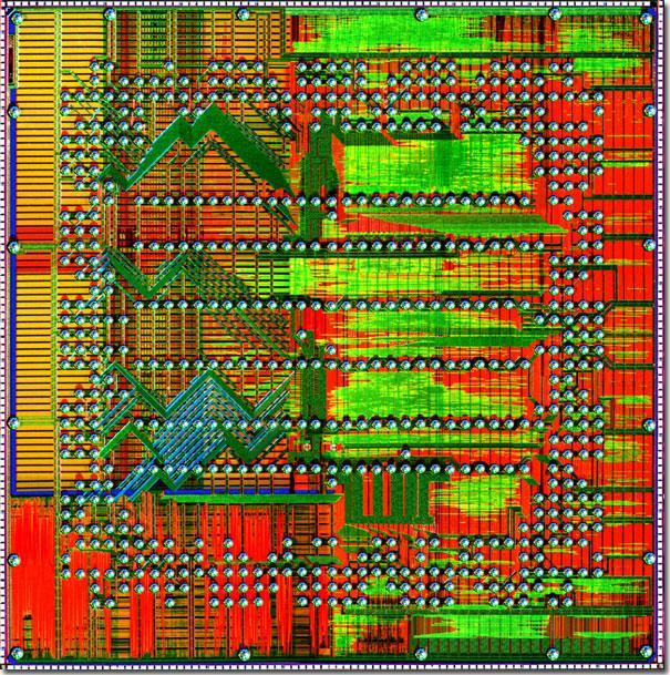
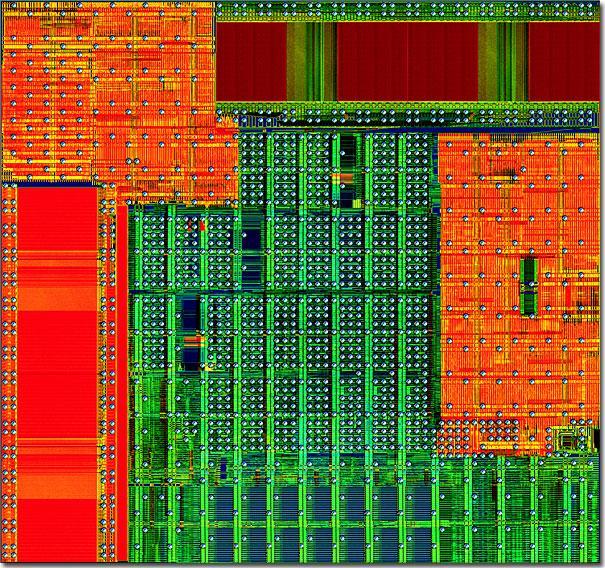


33 Field Effect Transistors IBM/Motorola Power PC620 IBM Power PC 601 Motorola MC68020 EE314

34 Chapter 12: Field Effect Transistors 1.Construction of MOS 2.NMOS and PMOS 3.Types of MOS 4.MOSFET Basic Operation 5.Characteristics
 & p-channel MOSFET")
35 The MOS Transistor Polysilicon Aluminum JFET Junction Field Effect Transistor MOSFET - Metal Oxide Semiconductor Field Effect Transistor n-channel MOSFET (nmos) & p-channel MOSFET (pmos)
36 The MOS Transistor Gate Oxide Gate Source n+ Polysilicon Drain n+ Field-Oxide (SiO 2 ) p-substrate p+ stopper Bulk Contact CROSS-SECTION of NMOS Transistor
37 Switch Model of NMOS Transistor V GS Gate Source (of carriers) Drain (of carriers) Open (off) (Gate = 0 ) Closed (on) (Gate = 1 ) R on V GS < V T V GS > V T
38 Switch Model of PMOS Transistor V GS Gate Source (of carriers) Drain (of carriers) Open (off) (Gate = 1 ) Closed (on) (Gate = 0 ) R on V GS > V DD V T V GS < V DD V T
39 MOS transistors Symbols D D G G S NMOS Enhancement NMOS D S Depletion D Channel G G B PMOS S Enhancement S NMOS with Bulk Contact

40 JFET and MOSFET Transistorsor Symbol L = m W = m SiO 2 Thickness = m Device characteristics depend on L,W, Thickness, doping levels

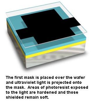
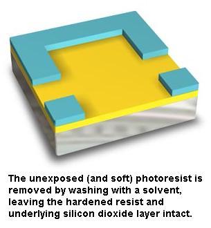
41 MOSFET Transistor Fabrication Steps


42 Building A MOSFET Transistor Using Silicon
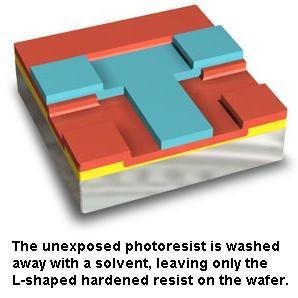
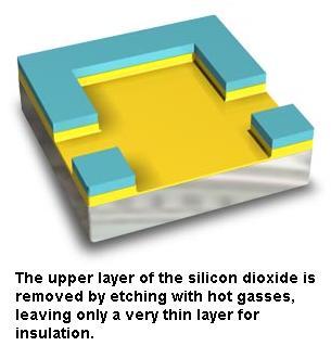
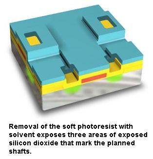
43
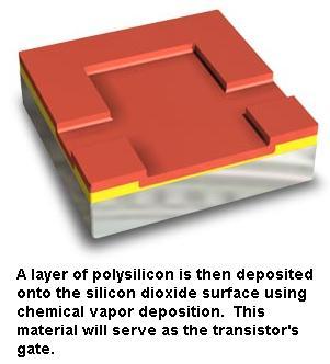
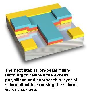
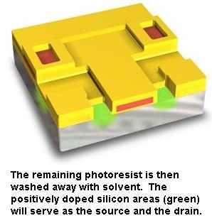
44
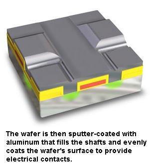
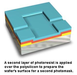
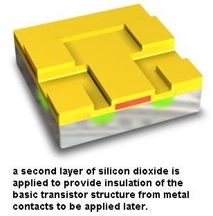
45


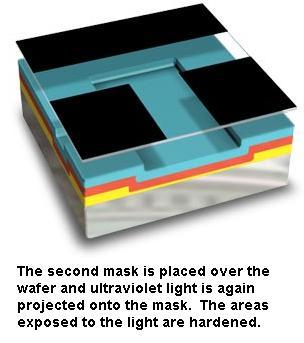
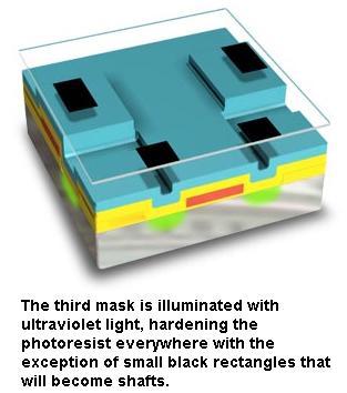
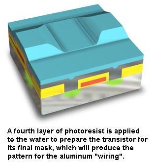
46 It is done. Now, how does it work?
47 n-channel MOSFET Basic Operation Operation in the Cutoff region pn junction: reverse bias i D =0 for v GS <V t0 Schematic When v GS =0 then i D =0 until v GS >V t0 (V t0 threshold voltage)
48 n-channel MOSFET Basic Operation Operation in the Triode Region For v DS <v GS -V t0 and v GS >V t0 the NMOS is operating in the triode region Resistor like characteristic (R between S & D, Used as voltage controlled R) For small v DS, i D is proportional to the excess voltage v GS -V t0
49 n-channel MOSFET Basic Operation Operation in the Triode Region i D K 2 2 vgs Vt0 vds vds K W L KP 2 Device parameter KP for NMOSFET is 50 A/V 2

50 n-channel MOSFET Basic Operation Operation in the Saturation Region (v DS is increased) Tapering of the channel - increments of i D are smaller when v DS is larger When v GD =V t0 then the channel thickness is 0 and i D K v GS V t0 2
51 n-channel MOSFET Basic Operation Example 12.1 An nmos has W=160 m, L=2 m, KP= 50 A/V 2 and V to =2 V. Plot the drain current characteristic vs drain to source voltage for v GS =3 V. i D i D K K 2 2 vgs Vt0 vds vds v GS V t0 2 K W L KP 2
52 n-channel MOSFET Basic Operation Example 12.1 Characteristic Channel length modulation i d depends on v DS in saturation region (approx: i D =const in saturation region) 2 i D Kv DS
53 p-channel MOSFET Basic Operation It is constructed by interchanging the n and p regions of n- channel MOSFET. Symbol Characteristic How does p-channel MOSFET operate? -voltage polarities -i D current -schematic


54 Fig. 5.1 Physical structure of the enhancement-type NMOS transistor: (a) perspective view; (b) cross section. Typically L = 1 to 10 m, W = 2 to 500 m, and the thickness of the oxide layer is in the range of 0.02 to 0.1 m.

55 Fig. 5.2 The enhancement-type NMOS transistor with a positive voltage applied to the gate. An n channel is induced at the top of the substrate beneath the gate.
 v DS.")
56 Fig. 5.3 An NMOS transistor with v GS > V t and with a small v DS applied. The device acts as a conductance whose value is determined by v GS. Specifically, the channel conductance is proportional to v GS - V t, and this i D is proportional to (v GS - Vt) v DS. Note that the depletion region is not shown (for simplicity).

57 Fig. 5.5 Operation of the enhancement NMOS transistor as v DS is increased. The induced channel acquires a tapered shape and its resistance increases as v DS is increased. Here, v GS is kept constant at a value > V t.
58 Fig. 5.6 The drain current i D versus the drain-to-source voltage v DS for an enhancement-type NMOS transistor operated with v GS > V t.
59 Fig. 5.8 Derivation of the i D - v DS characteristic of the NMOS transistor.

60 Fig. 5.9 Cross section of a CMOS integrated circuit. Note that the PMOS transistor is formed in a separate n-type region, known as an n well. Another arrangement is also possible in which an n-type body is used and the n device is formed in a p well.
61 Fig (a) An n-channel enhancement-type MOSFET with v GS and v DS applied and with the normal directions of current flow indicated. (b) The i D - v DS characteristics for a device with V t = 1 V and k n (W/L) = 0.5 ma/v 2.
62 Fig The i D - v GS characteristic for an enhancement-type NMOS transistor in saturation (V t = 1 V and k n (W/L) = 0.5 ma/v 2 ).

63 Fig Increasing v DS beyond v DSsat causes the channel pinch-off point to move slightly away from the drain, thus reducing the effective channel length (by L).
64 Fig Effect of v DS on i D in the saturation region. The MOSFET parameter V A is typically in the range of 30 to 200 V.


65 Fig Large-signal equivalent circuit model of the n-channel MOSFET in saturation, incorporating the output resistance r o. The output resistance models the linear dependence of i D on v DS and is given by r o V A/ I D.
66 Fig The current-voltage characteristics of a depletion-type n-channel MOSFET for which V t = -4 V and k n (W/L) = 2 ma/v 2 : (a) transistor with current and voltage polarities indicated; (b) the i D - v DS characteristics; (c) the i D - v GS characteristic in saturation.
67 Fig Conceptual circuit utilized to study the operation of the MOSFET as an amplifier.
68 Fig Small-signal operation of the enhancement MOSFET amplifier.
69 Fig Total instantaneous voltages v GS and v D for the circuit in Fig
 neglecting the dependence of i D on v DS in saturation (channel-length")
70 Fig Small-signal models for the MOSFET: (a) neglecting the dependence of i D on v DS in saturation (channel-length modulation effect); and (b) including the effect of channel-length modulation modeled by output resistance r o = V A / I D.

71 Fig the T model of the MOSFET augmented with the drain-to-source resistance ro.
72 Fig Basic MOSFET current mirror.
73 Fig Output characteristic of the current source in Fig and the current mirror of Fig for the case Q 2 is matched to Q 1.
74 Fig The CMOS common-source amplifier: (a) circuit; (b) i-v characteristic of the active-load Q 2 ; (c) graphical construction to determine the transfer characteristic; and transfer characteristic.
75 Fig The CMOS common-gate amplifier: (a) circuit; (b) small-signal equivalent circuit; and (c) simplified version of the circuit in (b).
76 Fig The source follower: (a) circuit; (b) small-signal equivalent circuit; and (c) simplified version of the equivalent circuit.
77 Fig (a) NMOS amplifier with enhancement load; (b) graphical determination of the transfer characteristic; (c) transfer characteristic.
78 Fig The NMOS amplifier with depletion load: (a) circuit; (b) graphical construction to determine the transfer characteristic; and (c) transfer characteristic.
79 Fig Small-signal equivalent circuit of the depletion-load amplifier of Fig (a), incorporating the body effect of Q 2.
80 Fig (a) The CMOS inverter. (b) Simplified circuit schematic for the inverter.
81 Fig Operation of the CMOS inverter when v 1 is high: (a) circuit with v 1 = V DD (logic-1 level, or V OH ); (b) graphical construction to determine the operating point; and (c) equivalent circuit.
82 Fig Operation of the CMOS inverter when v 1 is low: (a) circuit with v 1 = 0V (logic-0 level, or V OL ); (b) graphical construction to determine the operating point; and (c) equivalent circuit.
83 Fig The voltage transfer characteristic of the CMOS inverter.
84 Fig Dynamic operation of a capacitively loaded CMOS inverter: (a) circuit; (b) input and output waveforms; (c) trajectory of the operating point as the input goes high and C discharges through the Q N ; (d) equivalent circuit during the capacitor discharge.
85 Fig The CMOS transmission gate.
86 Fig Equivalent circuits for visualizing the operation of the transmission gate in the closed (on) position: (a) v A is positive; (b) v A is negative.
 High-frequency equivalent circuit")

 with")
87 Fig (a) High-frequency equivalent circuit model for the MOSFET; (b) the equivalent circuit for the case the source is connected to the substrate (body); (c) the equivalent circuit model of (b) with C db neglected (to simplify analysis).

88 Fig Determining the short-circuit current gain I o /I i.
I E I C since I B is very small
 Figure 2: Symbols and nomenclature of a (a) npn and (b) pnp transistor. The BJT consists of three regions, emitter, base, and collector. The emitter and collector are usually of one type of doping, while
BJT Amplifier. Superposition principle (linear amplifier)
") BJT Amplifier Two types analysis DC analysis Applied DC voltage source AC analysis Time varying signal source Superposition principle (linear amplifier) The response of a linear amplifier circuit excited
BJT Amplifier Two types analysis DC analysis Applied DC voltage source AC analysis Time varying signal source Superposition principle (linear amplifier) The response of a linear amplifier circuit excited
UNIT 3: FIELD EFFECT TRANSISTORS
 FIELD EFFECT TRANSISTOR: UNIT 3: FIELD EFFECT TRANSISTORS The field effect transistor is a semiconductor device, which depends for its operation on the control of current by an electric field. There are
Lecture 3: Transistors
 Lecture 3: Transistors Now that we know about diodes, let s put two of them together, as follows: collector base emitter n p n moderately doped lightly doped, and very thin heavily doped At first glance,
Field-Effect Transistor (FET) is one of the two major transistors; FET derives its name from its working mechanism;
 is one of the two major transistors; FET derives its name from its working mechanism;") Chapter 3 Field-Effect Transistors (FETs) 3.1 Introduction Field-Effect Transistor (FET) is one of the two major transistors; FET derives its name from its working mechanism; The concept has been known
Chapter 3 Field-Effect Transistors (FETs) 3.1 Introduction Field-Effect Transistor (FET) is one of the two major transistors; FET derives its name from its working mechanism; The concept has been known
Analog Electronics. Electronic Devices, 9th edition Thomas L. Floyd Pearson Education. Upper Saddle River, NJ, All rights reserved.
 Analog Electronics BJT Structure The BJT has three regions called the emitter, base, and collector. Between the regions are junctions as indicated. The base is a thin lightly doped region compared to the
MOSFET Terminals. The voltage applied to the GATE terminal determines whether current can flow between the SOURCE & DRAIN terminals.
 MOSFET Terminals The voltage applied to the GATE terminal determines whether current can flow between the SOURCE & DRAIN terminals. For an n-channel MOSFET, the SOURCE is biased at a lower potential (often
MEASUREMENT AND INSTRUMENTATION STUDY NOTES UNIT-I
 MEASUREMENT AND INSTRUMENTATION STUDY NOTES The MOSFET The MOSFET Metal Oxide FET UNIT-I As well as the Junction Field Effect Transistor (JFET), there is another type of Field Effect Transistor available
MOS Field-Effect Transistors (MOSFETs)
") 6 MOS Field-Effect Transistors (MOSFETs) A three-terminal device that uses the voltages of the two terminals to control the current flowing in the third terminal. The basis for amplifier design. The basis
6 MOS Field-Effect Transistors (MOSFETs) A three-terminal device that uses the voltages of the two terminals to control the current flowing in the third terminal. The basis for amplifier design. The basis
Three Terminal Devices
 Three Terminal Devices - field effect transistor (FET) - bipolar junction transistor (BJT) - foundation on which modern electronics is built - active devices - devices described completely by considering
INTRODUCTION TO MOS TECHNOLOGY
 INTRODUCTION TO MOS TECHNOLOGY 1. The MOS transistor The most basic element in the design of a large scale integrated circuit is the transistor. For the processes we will discuss, the type of transistor
Solid State Devices- Part- II. Module- IV
 Solid State Devices- Part- II Module- IV MOS Capacitor Two terminal MOS device MOS = Metal- Oxide- Semiconductor MOS capacitor - the heart of the MOSFET The MOS capacitor is used to induce charge at the
Field Effect Transistors
 Field Effect Transistors LECTURE NO. - 41 Field Effect Transistors www.mycsvtunotes.in JFET MOSFET CMOS Field Effect transistors - FETs First, why are we using still another transistor? BJTs had a small
Design cycle for MEMS
 Design cycle for MEMS Design cycle for ICs IC Process Selection nmos CMOS BiCMOS ECL for logic for I/O and driver circuit for critical high speed parts of the system The Real Estate of a Wafer MOS Transistor
COLLECTOR DRAIN BASE GATE EMITTER. Applying a voltage to the Gate connection allows current to flow between the Drain and Source connections.
 MOSFETS Although the base current in a transistor is usually small (< 0.1 ma), some input devices (e.g. a crystal microphone) may be limited in their output. In order to overcome this, a Field Effect Transistor
Digital Electronics. By: FARHAD FARADJI, Ph.D. Assistant Professor, Electrical and Computer Engineering, K. N. Toosi University of Technology
 K. N. Toosi University of Technology Chapter 7. Field-Effect Transistors By: FARHAD FARADJI, Ph.D. Assistant Professor, Electrical and Computer Engineering, K. N. Toosi University of Technology http://wp.kntu.ac.ir/faradji/digitalelectronics.htm
EE105 Fall 2015 Microelectronic Devices and Circuits
 EE105 Fall 2015 Microelectronic Devices and Circuits Prof. Ming C. Wu wu@eecs.berkeley.edu 511 Sutardja Dai Hall (SDH) 11-1 Transistor Operating Mode in Amplifiers Transistors are biased in flat part of
Laboratory #5 BJT Basics and MOSFET Basics
 Laboratory #5 BJT Basics and MOSFET Basics I. Objectives 1. Understand the physical structure of BJTs and MOSFETs. 2. Learn to measure I-V characteristics of BJTs and MOSFETs. II. Components and Instruments
Lecture-45. MOS Field-Effect-Transistors Threshold voltage
 Lecture-45 MOS Field-Effect-Transistors 7.4. Threshold voltage In this section we summarize the calculation of the threshold voltage and discuss the dependence of the threshold voltage on the bias applied
EIE209 Basic Electronics. Transistor Devices. Contents BJT and FET Characteristics Operations. Prof. C.K. Tse: T ransistor devices
 EIE209 Basic Electronics Transistor Devices Contents BJT and FET Characteristics Operations 1 What is a transistor? Three-terminal device whose voltage-current relationship is controlled by a third voltage
ES 330 Electronics II Homework # 2 (Fall 2016 Due Wednesday, September 7, 2016)
") Page1 Name ES 330 Electronics II Homework # 2 (Fall 2016 Due Wednesday, September 7, 2016) Problem 1 (15 points) You are given an NMOS amplifier with drain load resistor R D = 20 k. The DC voltage (V RD
Page1 Name ES 330 Electronics II Homework # 2 (Fall 2016 Due Wednesday, September 7, 2016) Problem 1 (15 points) You are given an NMOS amplifier with drain load resistor R D = 20 k. The DC voltage (V RD
8. Characteristics of Field Effect Transistor (MOSFET)
") 1 8. Characteristics of Field Effect Transistor (MOSFET) 8.1. Objectives The purpose of this experiment is to measure input and output characteristics of n-channel and p- channel field effect transistors
1 8. Characteristics of Field Effect Transistor (MOSFET) 8.1. Objectives The purpose of this experiment is to measure input and output characteristics of n-channel and p- channel field effect transistors
Bipolar Junction Transistors (BJTs)
") C H A P T E R 6 Bipolar Junction Transistors (BJTs) Figure 6.1 A simplified structure of the npn transistor and pnp transistor. Table 6.1: BJT modes of Operation Mode Cutoff Active Saturation EBJ Reverse
C H A P T E R 6 Bipolar Junction Transistors (BJTs) Figure 6.1 A simplified structure of the npn transistor and pnp transistor. Table 6.1: BJT modes of Operation Mode Cutoff Active Saturation EBJ Reverse
Electronic Circuits for Mechatronics ELCT 609 Lecture 6: MOS-FET Transistor
 Electronic Circuits for Mechatronics ELCT 609 Lecture 6: MOS-FET Transistor Assistant Professor Office: C3.315 E-mail: eman.azab@guc.edu.eg 1 Introduction Why we call it Transistor? The name came as an
FET. Field Effect Transistors ELEKTRONIKA KONTROL. Eka Maulana, ST, MT, M.Eng. Universitas Brawijaya. p + S n n-channel. Gate. Basic structure.
 FET Field Effect Transistors ELEKTRONIKA KONTROL Basic structure Gate G Source S n n-channel Cross section p + p + p + G Depletion region Drain D Eka Maulana, ST, MT, M.Eng. Universitas Brawijaya S Channel
Student Lecture by: Giangiacomo Groppi Joel Cassell Pierre Berthelot September 28 th 2004
 Student Lecture by: Giangiacomo Groppi Joel Cassell Pierre Berthelot September 28 th 2004 Lecture outline Historical introduction Semiconductor devices overview Bipolar Junction Transistor (BJT) Field
UNIT-VI FIELD EFFECT TRANSISTOR. 1. Explain about the Field Effect Transistor and also mention types of FET s.
 UNIT-I FIELD EFFECT TRANSISTOR 1. Explain about the Field Effect Transistor and also mention types of FET s. The Field Effect Transistor, or simply FET however, uses the voltage that is applied to their
F7 Transistor Amplifiers
 Lars Ohlsson 2018-09-25 F7 Transistor Amplifiers Outline Transfer characteristics Small signal operation and models Basic configurations Common source (CS) CS/CE w/ source/ emitter degeneration resistance
Prof. Paolo Colantonio a.a
 Prof. Paolo Colantonio a.a. 20 2 Field effect transistors (FETs) are probably the simplest form of transistor, widely used in both analogue and digital applications They are characterised by a very high
EE301 Electronics I , Fall
 EE301 Electronics I 2018-2019, Fall 1. Introduction to Microelectronics (1 Week/3 Hrs.) Introduction, Historical Background, Basic Consepts 2. Rewiev of Semiconductors (1 Week/3 Hrs.) Semiconductor materials
Bipolar junction transistors.
 Bipolar junction transistors. Third Semester Course code : 15EECC202 Analog electronic circuits (AEC) Team: Dr. Nalini C Iyer, R.V. Hangal, Sujata N, Prashant A, Sneha Meti AEC Team, Faculty, School of
Gechstudentszone.wordpress.com
 UNIT 4: Small Signal Analysis of Amplifiers 4.1 Basic FET Amplifiers In the last chapter, we described the operation of the FET, in particular the MOSFET, and analyzed and designed the dc response of circuits
Tema 12 Transistores. 12.a. El transistor bipolar 12.b. El transistor MOS
 Tema 12 Transistores. 12.a. El transistor bipolar 12.b. El transistor MOS 1 Capítulo12.a El Transistor Bipolar 2 El transistor bipolar de unión, BT, npn Figure 5.1 A simplified structure of the npn transistor.
Bipolar Junction Transistors (BJTs) Overview
 Overview") 1 Bipolar Junction Transistors (BJTs) Asst. Prof. MONTREE SIRIPRUCHYANUN, D. Eng. Dept. of Teacher Training in Electrical Engineering, Faculty of Technical Education King Mongkut s Institute of Technology
1 Bipolar Junction Transistors (BJTs) Asst. Prof. MONTREE SIRIPRUCHYANUN, D. Eng. Dept. of Teacher Training in Electrical Engineering, Faculty of Technical Education King Mongkut s Institute of Technology
Figure1: Basic BJT construction.
 Chapter 4: Bipolar Junction Transistors (BJTs) Bipolar Junction Transistor (BJT) Structure The BJT is constructed with three doped semiconductor regions separated by two pn junctions, as in Figure 1(a).
MOSFET & IC Basics - GATE Problems (Part - I)
") MOSFET & IC Basics - GATE Problems (Part - I) 1. Channel current is reduced on application of a more positive voltage to the GATE of the depletion mode n channel MOSFET. (True/False) [GATE 1994: 1 Mark]
MOSFET & IC Basics - GATE Problems (Part - I) 1. Channel current is reduced on application of a more positive voltage to the GATE of the depletion mode n channel MOSFET. (True/False) [GATE 1994: 1 Mark]
6. Field-Effect Transistor
 6. Outline: Introduction to three types of FET: JFET MOSFET & CMOS MESFET Constructions, Characteristics & Transfer curves of: JFET & MOSFET Introduction The field-effect transistor (FET) is a threeterminal
C H A P T E R 6 Bipolar Junction Transistors (BJTs)
") C H A P T E R 6 Bipolar Junction Transistors (BJTs) Figure 6.1 A simplified structure of the npn transistor and pnp transistor. Table 6.1: BJT modes of Operation Mode EBJ CBJ Cutoff Reverse Reverse Active
C H A P T E R 6 Bipolar Junction Transistors (BJTs) Figure 6.1 A simplified structure of the npn transistor and pnp transistor. Table 6.1: BJT modes of Operation Mode EBJ CBJ Cutoff Reverse Reverse Active
EE105 Fall 2015 Microelectronic Devices and Circuits: MOSFET Prof. Ming C. Wu 511 Sutardja Dai Hall (SDH)
") EE105 Fall 2015 Microelectronic Devices and Circuits: MOSFET Prof. Ming C. Wu wu@eecs.berkeley.edu 511 Sutardja Dai Hall (SDH) 7-1 Simplest Model of MOSFET (from EE16B) 7-2 CMOS Inverter 7-3 CMOS NAND
EE105 Fall 2015 Microelectronic Devices and Circuits: MOSFET Prof. Ming C. Wu wu@eecs.berkeley.edu 511 Sutardja Dai Hall (SDH) 7-1 Simplest Model of MOSFET (from EE16B) 7-2 CMOS Inverter 7-3 CMOS NAND
Lecture 24: Bipolar Junction Transistors (1) Bipolar Junction Structure, Operating Regions, Biasing
 Bipolar Junction Structure, Operating Regions, Biasing") Lecture 24: Bipolar Junction Transistors (1) Bipolar Junction Structure, Operating Regions, Biasing BJT Structure the BJT is formed by doping three semiconductor regions (emitter, base, and collector)
Lecture 24: Bipolar Junction Transistors (1) Bipolar Junction Structure, Operating Regions, Biasing BJT Structure the BJT is formed by doping three semiconductor regions (emitter, base, and collector)
Introduction to MOSFET MOSFET (Metal Oxide Semiconductor Field Effect Transistor)
") Microelectronic Circuits Introduction to MOSFET MOSFET (Metal Oxide Semiconductor Field Effect Transistor) Slide 1 MOSFET Construction MOSFET (Metal Oxide Semiconductor Field Effect Transistor) Slide 2
Microelectronic Circuits Introduction to MOSFET MOSFET (Metal Oxide Semiconductor Field Effect Transistor) Slide 1 MOSFET Construction MOSFET (Metal Oxide Semiconductor Field Effect Transistor) Slide 2
EE 5611 Introduction to Microelectronic Technologies Fall Thursday, September 04, 2014 Lecture 02
 EE 5611 Introduction to Microelectronic Technologies Fall 2014 Thursday, September 04, 2014 Lecture 02 1 Lecture Outline Review on semiconductor materials Review on microelectronic devices Example of microelectronic
Basic Electronics Prof. Dr. Chitralekha Mahanta Department of Electronics and Communication Engineering Indian Institute of Technology, Guwahati
 Basic Electronics Prof. Dr. Chitralekha Mahanta Department of Electronics and Communication Engineering Indian Institute of Technology, Guwahati Module: 3 Field Effect Transistors Lecture-7 High Frequency
Electronic Circuits for Mechatronics ELCT 609 Lecture 7: MOS-FET Amplifiers
 Electronic Circuits for Mechatronics ELCT 609 Lecture 7: MOS-FET Amplifiers Assistant Professor Office: C3.315 E-mail: eman.azab@guc.edu.eg 1 Enhancement N-MOS Modes of Operation Mode V GS I DS V DS Cutoff
ECE 442 Solid State Devices & Circuits. 15. Differential Amplifiers
 ECE 442 Solid State Devices & Circuits 15. Differential Amplifiers Jose E. Schutt-Aine Electrical & Computer Engineering University of Illinois jschutt@emlab.uiuc.edu ECE 442 Jose Schutt Aine 1 Background
Depletion-mode operation ( 공핍형 ): Using an input gate voltage to effectively decrease the channel size of an FET
: Using an input gate voltage to effectively decrease the channel size of an FET") Ch. 13 MOSFET Metal-Oxide-Semiconductor Field-Effect Transistor : I D D-mode E-mode V g The gate oxide is made of dielectric SiO 2 with e = 3.9 Depletion-mode operation ( 공핍형 ): Using an input gate voltage
Ch. 13 MOSFET Metal-Oxide-Semiconductor Field-Effect Transistor : I D D-mode E-mode V g The gate oxide is made of dielectric SiO 2 with e = 3.9 Depletion-mode operation ( 공핍형 ): Using an input gate voltage
Semiconductor Physics and Devices
 Metal-Semiconductor and Semiconductor Heterojunctions The Metal-Oxide-Semiconductor Field-Effect Transistor (MOSFET) is one of two major types of transistors. The MOSFET is used in digital circuit, because
Lecture - 18 Transistors
 Electronic Materials, Devices and Fabrication Dr. S. Prarasuraman Department of Metallurgical and Materials Engineering Indian Institute of Technology, Madras Lecture - 18 Transistors Last couple of classes
Chapter 2 : Semiconductor Materials & Devices (II) Feb
 Feb") Chapter 2 : Semiconductor Materials & Devices (II) 1 Reference 1. SemiconductorManufacturing Technology: Michael Quirk and Julian Serda (2001) 3. Microelectronic Circuits (5/e): Sedra & Smith (2004) 4.
Chapter 2 : Semiconductor Materials & Devices (II) 1 Reference 1. SemiconductorManufacturing Technology: Michael Quirk and Julian Serda (2001) 3. Microelectronic Circuits (5/e): Sedra & Smith (2004) 4.
EE70 - Intro. Electronics
 EE70 - Intro. Electronics Course website: ~/classes/ee70/fall05 Today s class agenda (November 28, 2005) review Serial/parallel resonant circuits Diode Field Effect Transistor (FET) f 0 = Qs = Qs = 1 2π
FIELD EFFECT TRANSISTOR (FET) 1. JUNCTION FIELD EFFECT TRANSISTOR (JFET)
 1. JUNCTION FIELD EFFECT TRANSISTOR (JFET)") FIELD EFFECT TRANSISTOR (FET) The field-effect transistor (FET) is a three-terminal device used for a variety of applications that match, to a large extent, those of the BJT transistor. Although there
FIELD EFFECT TRANSISTOR (FET) The field-effect transistor (FET) is a three-terminal device used for a variety of applications that match, to a large extent, those of the BJT transistor. Although there
INTRODUCTION: Basic operating principle of a MOSFET:
 INTRODUCTION: Along with the Junction Field Effect Transistor (JFET), there is another type of Field Effect Transistor available whose Gate input is electrically insulated from the main current carrying
CHAPTER 8 FIELD EFFECT TRANSISTOR (FETs)
") CHAPTER 8 FIELD EFFECT TRANSISTOR (FETs) INTRODUCTION - FETs are voltage controlled devices as opposed to BJT which are current controlled. - There are two types of FETs. o Junction FET (JFET) o Metal
CHAPTER 8 FIELD EFFECT TRANSISTOR (FETs) INTRODUCTION - FETs are voltage controlled devices as opposed to BJT which are current controlled. - There are two types of FETs. o Junction FET (JFET) o Metal
UNIT 3 Transistors JFET
 UNIT 3 Transistors JFET Mosfet Definition of BJT A bipolar junction transistor is a three terminal semiconductor device consisting of two p-n junctions which is able to amplify or magnify a signal. It
Device Technologies. Yau - 1
 Device Technologies Yau - 1 Objectives After studying the material in this chapter, you will be able to: 1. Identify differences between analog and digital devices and passive and active components. Explain
UNIT I BIASING OF DISCRETE BJT AND MOSFET PART A
 UNIT I BIASING OF DISCRETE BJT AND MOSFET PART A 1. Why do we choose Q point at the center of the load line? 2. Name the two techniques used in the stability of the q point.explain. 3. Give the expression
ENEE 307 Laboratory#2 (n-mosfet, p-mosfet, and a single n-mosfet amplifier in the common source configuration)
") Revised 2/16/2007 ENEE 307 Laboratory#2 (n-mosfet, p-mosfet, and a single n-mosfet amplifier in the common source configuration) *NOTE: The text mentioned below refers to the Sedra/Smith, 5th edition.
Revised 2/16/2007 ENEE 307 Laboratory#2 (n-mosfet, p-mosfet, and a single n-mosfet amplifier in the common source configuration) *NOTE: The text mentioned below refers to the Sedra/Smith, 5th edition.
UNIVERSITY OF CALIFORNIA AT BERKELEY College of Engineering Department of Electrical Engineering and Computer Sciences.
 UNIVERSITY OF CALIFORNIA AT BERKELEY College of Engineering Department of Electrical Engineering and Computer Sciences Discussion #9 EE 05 Spring 2008 Prof. u MOSFETs The standard MOSFET structure is shown
4.2.2 Metal Oxide Semiconductor Field Effect Transistor (MOSFET)
") 4.2.2 Metal Oxide Semiconductor Field Effect Transistor (MOSFET) The Metal Oxide Semitonductor Field Effect Transistor (MOSFET) has two modes of operation, the depletion mode, and the enhancement mode.
4.2.2 Metal Oxide Semiconductor Field Effect Transistor (MOSFET) The Metal Oxide Semitonductor Field Effect Transistor (MOSFET) has two modes of operation, the depletion mode, and the enhancement mode.
55:041 Electronic Circuits
 55:041 Electronic Circuits MOSFETs Sections of Chapter 3 &4 A. Kruger MOSFETs, Page-1 Basic Structure of MOS Capacitor Sect. 3.1 Width = 1 10-6 m or less Thickness = 50 10-9 m or less ` MOS Metal-Oxide-Semiconductor
55:041 Electronic Circuits
 55:041 Electronic Circuits Mosfet Review Sections of Chapter 3 &4 A. Kruger Mosfet Review, Page-1 Basic Structure of MOS Capacitor Sect. 3.1 Width 1 10-6 m or less Thickness 50 10-9 m or less ` MOS Metal-Oxide-Semiconductor
Solid State Devices & Circuits. 18. Advanced Techniques
 ECE 442 Solid State Devices & Circuits 18. Advanced Techniques Jose E. Schutt-Aine Electrical l&c Computer Engineering i University of Illinois jschutt@emlab.uiuc.edu 1 Darlington Configuration - Popular
Electronic Circuits EE359A
 Electronic Circuits EE359A Bruce McNair B206 bmcnair@stevens.edu 201-216-5549 Lecture 4 0 Bipolar Junction Transistors (BJT) Small Signal Analysis Graphical Analysis / Biasing Amplifier, Switch and Logic
Chapter 5: Field Effect Transistors
 Chapter 5: Field Effect Transistors Slide 1 FET FET s (Field Effect Transistors) are much like BJT s (Bipolar Junction Transistors). Similarities: Amplifiers Switching devices Impedance matching circuits
ECE520 VLSI Design. Lecture 2: Basic MOS Physics. Payman Zarkesh-Ha
 ECE520 VLSI Design Lecture 2: Basic MOS Physics Payman Zarkesh-Ha Office: ECE Bldg. 230B Office hours: Wednesday 2:00-3:00PM or by appointment E-mail: pzarkesh@unm.edu Slide: 1 Review of Last Lecture Semiconductor
Difference between BJTs and FETs. Junction Field Effect Transistors (JFET)
") Difference between BJTs and FETs Transistors can be categorized according to their structure, and two of the more commonly known transistor structures, are the BJT and FET. The comparison between BJTs
Difference between BJTs and FETs Transistors can be categorized according to their structure, and two of the more commonly known transistor structures, are the BJT and FET. The comparison between BJTs
Microelectronics Circuit Analysis and Design
 Microelectronics Circuit Analysis and Design Donald A. Neamen Chapter 3 The Field Effect Transistor Neamen Microelectronics, 4e Chapter 3-1 In this chapter, we will: Study and understand the operation
ITT Technical Institute. ET215 Devices 1. Unit 7 Chapter 4, Sections
 ITT Technical Institute ET215 Devices 1 Unit 7 Chapter 4, Sections 4.1 4.3 Chapter 4 Section 4.1 Structure of Field-Effect Transistors Recall that the BJT is a current-controlling device; the field-effect
Microelectronic Circuits, Kyung Hee Univ. Spring, Bipolar Junction Transistors
 Bipolar Junction Transistors 1 Introduction physical structure of the bipolar transistor and how it works How the voltage between two terminals of the transistor controls the current that flows through
Microelectronics Circuit Analysis and Design. MOS Capacitor Under Bias: Electric Field and Charge. Basic Structure of MOS Capacitor 9/25/2013
 Microelectronics Circuit Analysis and Design Donald A. Neamen Chapter 3 The Field Effect Transistor In this chapter, we will: Study and understand the operation and characteristics of the various types
Unit III FET and its Applications. 2 Marks Questions and Answers
 Unit III FET and its Applications 2 Marks Questions and Answers 1. Why do you call FET as field effect transistor? The name field effect is derived from the fact that the current is controlled by an electric
V A ( ) 2 = A. For Vbe = 0.4V: Ic = 7.34 * 10-8 A. For Vbe = 0.5V: Ic = 3.49 * 10-6 A. For Vbe = 0.6V: Ic = 1.
 2 = A. For Vbe = 0.4V: Ic = 7.34 * 10-8 A. For Vbe = 0.5V: Ic = 3.49 * 10-6 A. For Vbe = 0.6V: Ic = 1.") 1. A BJT has the structure and parameters below. a. Base Width = 0.5mu b. Electron lifetime in base is 1x10⁻⁷ sec c. Base doping is NA=10 17 /cm 3 d. Emitter Doping is ND=2 x10 19 /cm 3. Collector Doping
1. A BJT has the structure and parameters below. a. Base Width = 0.5mu b. Electron lifetime in base is 1x10⁻⁷ sec c. Base doping is NA=10 17 /cm 3 d. Emitter Doping is ND=2 x10 19 /cm 3. Collector Doping
MODULE-2: Field Effect Transistors (FET)
") FORMAT-1B Definition: MODULE-2: Field Effect Transistors (FET) FET is a three terminal electronic device used for variety of applications that match with BJT. In FET, an electric field is established by
FORMAT-1B Definition: MODULE-2: Field Effect Transistors (FET) FET is a three terminal electronic device used for variety of applications that match with BJT. In FET, an electric field is established by
Chapter 8. Field Effect Transistor
 Chapter 8. Field Effect Transistor Field Effect Transistor: The field effect transistor is a semiconductor device, which depends for its operation on the control of current by an electric field. There
Chapter Two "Bipolar Transistor Circuits"
 Chapter Two "Bipolar Transistor Circuits" 1.TRANSISTOR CONSTRUCTION:- The transistor is a three-layer semiconductor device consisting of either two n- and one p-type layers of material or two p- and one
Lesson 5. Electronics: Semiconductors Doping p-n Junction Diode Half Wave and Full Wave Rectification Introduction to Transistors-
 Lesson 5 Electronics: Semiconductors Doping p-n Junction Diode Half Wave and Full Wave Rectification Introduction to Transistors- Types and Connections Semiconductors Semiconductors If there are many free
Week 7: Common-Collector Amplifier, MOS Field Effect Transistor
 EE 2110A Electronic Circuits Week 7: Common-Collector Amplifier, MOS Field Effect Transistor ecture 07-1 Topics to coer Common-Collector Amplifier MOS Field Effect Transistor Physical Operation and I-V
UNIT I - TRANSISTOR BIAS STABILITY
 UNIT I - TRANSISTOR BIAS STABILITY OBJECTIVE On the completion of this unit the student will understand NEED OF BIASING CONCEPTS OF LOAD LINE Q-POINT AND ITS STABILIZATION AND COMPENSATION DIFFERENT TYPES
Week 9a OUTLINE. MOSFET I D vs. V GS characteristic Circuit models for the MOSFET. Reading. resistive switch model small-signal model
 Week 9a OUTLINE MOSFET I vs. V GS characteristic Circuit models for the MOSFET resistive switch model small-signal model Reading Rabaey et al.: Chapter 3.3.2 Hambley: Chapter 12 (through 12.5); Section
Chapter 6: Field-Effect Transistors
 Chapter 6: Field-Effect Transistors Islamic University of Gaza Dr. Talal Skaik MOSFETs MOSFETs have characteristics similar to JFETs and additional characteristics that make then very useful. There are
Conduction Characteristics of MOS Transistors (for fixed Vds)! Topic 2. Basic MOS theory & SPICE simulation. MOS Transistor
! Topic 2. Basic MOS theory & SPICE simulation. MOS Transistor") Conduction Characteristics of MOS Transistors (for fixed Vds)! Topic 2 Basic MOS theory & SPICE simulation Peter Cheung Department of Electrical & Electronic Engineering Imperial College London (Weste&Harris,
Conduction Characteristics of MOS Transistors (for fixed Vds)! Topic 2 Basic MOS theory & SPICE simulation Peter Cheung Department of Electrical & Electronic Engineering Imperial College London (Weste&Harris,
Topic 2. Basic MOS theory & SPICE simulation
 Topic 2 Basic MOS theory & SPICE simulation Peter Cheung Department of Electrical & Electronic Engineering Imperial College London (Weste&Harris, Ch 2 & 5.1-5.3 Rabaey, Ch 3) URL: www.ee.ic.ac.uk/pcheung/
Conduction Characteristics of MOS Transistors (for fixed Vds) Topic 2. Basic MOS theory & SPICE simulation. MOS Transistor
 Topic 2. Basic MOS theory & SPICE simulation. MOS Transistor") Conduction Characteristics of MOS Transistors (for fixed Vds) Topic 2 Basic MOS theory & SPICE simulation Peter Cheung Department of Electrical & Electronic Engineering Imperial College London (Weste&Harris,
Conduction Characteristics of MOS Transistors (for fixed Vds) Topic 2 Basic MOS theory & SPICE simulation Peter Cheung Department of Electrical & Electronic Engineering Imperial College London (Weste&Harris,
BJT. Bipolar Junction Transistor BJT BJT 11/6/2018. Dr. Satish Chandra, Assistant Professor, P P N College, Kanpur 1
 BJT Bipolar Junction Transistor Satish Chandra Assistant Professor Department of Physics P P N College, Kanpur www.satish0402.weebly.com The Bipolar Junction Transistor is a semiconductor device which
The shape of the waveform will be the same, but its level is shifted either upward or downward. The values of the resistor R and capacitor C affect
 Diode as Clamper A clamping circuit is used to place either the positive or negative peak of a signal at a desired level. The dc component is simply added or subtracted to/from the input signal. The clamper
(Refer Slide Time: 02:05)
") Electronics for Analog Signal Processing - I Prof. K. Radhakrishna Rao Department of Electrical Engineering Indian Institute of Technology Madras Lecture 27 Construction of a MOSFET (Refer Slide Time:
Electronics for Analog Signal Processing - I Prof. K. Radhakrishna Rao Department of Electrical Engineering Indian Institute of Technology Madras Lecture 27 Construction of a MOSFET (Refer Slide Time:
Course Outline. 4. Chapter 5: MOS Field Effect Transistors (MOSFET) 5. Chapter 6: Bipolar Junction Transistors (BJT)
 5. Chapter 6: Bipolar Junction Transistors (BJT)") Course Outline 1. Chapter 1: Signals and Amplifiers 1 2. Chapter 3: Semiconductors 3. Chapter 4: Diodes 4. Chapter 5: MOS Field Effect Transistors (MOSFET) 5. Chapter 6: Bipolar Junction Transistors (BJT)
Course Outline 1. Chapter 1: Signals and Amplifiers 1 2. Chapter 3: Semiconductors 3. Chapter 4: Diodes 4. Chapter 5: MOS Field Effect Transistors (MOSFET) 5. Chapter 6: Bipolar Junction Transistors (BJT)
Metal Oxide Semiconductor Field-Effect Transistors (MOSFETs)
") Metal Oxide Semiconductor Field-Effect Transistors (MOSFETs) Device Structure N-Channel MOSFET Providing electrons Pulling electrons (makes current flow) + + + Apply positive voltage to gate: Drives away
Metal Oxide Semiconductor Field-Effect Transistors (MOSFETs) Device Structure N-Channel MOSFET Providing electrons Pulling electrons (makes current flow) + + + Apply positive voltage to gate: Drives away
Chapter 6: Field-Effect Transistors
 Chapter 6: Field-Effect Transistors FETs vs. BJTs Similarities: Amplifiers Switching devices Impedance matching circuits Differences: FETs are voltage controlled devices. BJTs are current controlled devices.
Shankersinh Vaghela Bapu Institute of Technology INDEX
 Shankersinh Vaghela Bapu Institute of Technology Diploma EE Semester III 3330905: ELECTRONIC COMPONENTS AND CIRCUITS INDEX Sr. No. Title Page Date Sign Grade 1 Obtain I-V characteristic of Diode. 2 To
Basic Electronics. Introductory Lecture Course for. Technology and Instrumentation in Particle Physics Chicago, Illinois June 9-14, 2011
 Basic Electronics Introductory Lecture Course for Technology and Instrumentation in Particle Physics 2011 Chicago, Illinois June 9-14, 2011 Presented By Gary Drake Argonne National Laboratory Session 3
Lecture 16: MOS Transistor models: Linear models, SPICE models. Context. In the last lecture, we discussed the MOS transistor, and
 Lecture 16: MOS Transistor models: Linear models, SPICE models Context In the last lecture, we discussed the MOS transistor, and added a correction due to the changing depletion region, called the body
Field - Effect Transistor
 Page 1 of 6 Field - Effect Transistor Aim :- To draw and study the out put and transfer characteristics of the given FET and to determine its parameters. Apparatus :- FET, two variable power supplies,
AE103 ELECTRONIC DEVICES & CIRCUITS DEC 2014
 Q.2 a. State and explain the Reciprocity Theorem and Thevenins Theorem. a. Reciprocity Theorem: If we consider two loops A and B of network N and if an ideal voltage source E in loop A produces current
Electronic Circuits II - Revision
 Electronic Circuits II - Revision -1 / 16 - T & F # 1 A bypass capacitor in a CE amplifier decreases the voltage gain. 2 If RC in a CE amplifier is increased, the voltage gain is reduced. 3 4 5 The load
MTLE-6120: Advanced Electronic Properties of Materials. Semiconductor transistors for logic and memory. Reading: Kasap
 MTLE-6120: Advanced Electronic Properties of Materials 1 Semiconductor transistors for logic and memory Reading: Kasap 6.6-6.8 Vacuum tube diodes 2 Thermionic emission from cathode Electrons collected
Bipolar Junction Transistor (BJT) Basics- GATE Problems
 Basics- GATE Problems") Bipolar Junction Transistor (BJT) Basics- GATE Problems One Mark Questions 1. The break down voltage of a transistor with its base open is BV CEO and that with emitter open is BV CBO, then (a) BV CEO =
Bipolar Junction Transistor (BJT) Basics- GATE Problems One Mark Questions 1. The break down voltage of a transistor with its base open is BV CEO and that with emitter open is BV CBO, then (a) BV CEO =
Field Effect Transistors
 Chapter 5: Field Effect Transistors Slide 1 FET FET s (Field Effect Transistors) are much like BJT s (Bipolar Junction Transistors). Similarities: Amplifiers Switching devices Impedance matching circuits
Bipolar Junction Transistors
 Bipolar Junction Transistors Invented in 1948 at Bell Telephone laboratories Bipolar junction transistor (BJT) - one of the major three terminal devices Three terminal devices more useful than two terminal
SRM INSTITUTE OF SCIENCE AND TECHNOLOGY (DEEMED UNIVERSITY)
") SRM INSTITUTE OF SCIENCE AND TECHNOLOGY (DEEMED UNIVERSITY) QUESTION BANK I YEAR B.Tech (II Semester) ELECTRONIC DEVICES (COMMON FOR EC102, EE104, IC108, BM106) UNIT-I PART-A 1. What are intrinsic and
SRM INSTITUTE OF SCIENCE AND TECHNOLOGY (DEEMED UNIVERSITY) QUESTION BANK I YEAR B.Tech (II Semester) ELECTRONIC DEVICES (COMMON FOR EC102, EE104, IC108, BM106) UNIT-I PART-A 1. What are intrinsic and