Solid State Devices & Circuits. 18. Advanced Techniques
|
|
|
- Isabella Carr
- 5 years ago
- Views:
Transcription
1 ECE 442 Solid State Devices & Circuits 18. Advanced Techniques Jose E. Schutt-Aine Electrical l&c Computer Engineering i University of Illinois jschutt@emlab.uiuc.edu 1
2 Darlington Configuration - Popular BJT combination - Composite transistor with = Can be used as the cascade of two CC 2
3 Darlington Voltage Follower R 1 r 1 r R in e1 2 e2 E / 1 e1 sig 1 Rout R E // re v v out sig R E r e2 r r R R E R e1 sig / 1 3
4 Darlington Voltage Follower Darlington follower presents high input impedance 4
5 Darlington Voltage Follower Input impedance R 1 r1 2 1 r 2 R in e e E Output t impedance R R // r Voltage gain: A MB out E e 2 R r R /( 1) 1 e1 sig RE re2 re 1Rsig /( 1 1) /( 2 1) E 5
6 Op Amp Architecture Concepts - Many op amps consist of 3 amplifying stages - The first stage is always a high-gain differential stage - The second stage has moderate value of voltage gain - The last stage is often a buffer stage with high current gain and voltage gain near unity - The high-frequency poles of each stage introduce phase shift at higher frequenciesmay lead to oscillations 6
7 Op Amp Specifications Specifications - Input Offset Voltage (V os ) - Input Offset Voltage Drift (TCV os ) - Input Bias Current (I B ) - Input Offset Current (I os ) - Common-Mode Input Voltage Range (CMVR) - Common-Mode Rejection Ratio (CMRR) - Power Supply Rejection Ratio (PSRR) 7
8 CMOS OP Amp Example In the differential amplifier shown, Q 1 and Q 2 form the differential pair while the current source transistors Q 4 and Q 5 form the active loads for Q 1 and Q 2 respectively. The dc bias circuit that establishes an appropriate dc voltage at the drains of Q 1 and Q 2 is not shown. The following specifications are desired: differential gain A d = 80V/V, I REF = 100 A, the dc voltage at the gates of Q 6 and Q 3 is +1.5V; the dc voltage at the gates of Q 7, Q 4 and Q 5 is 1.5V. The technology available is specified as follows: n C ox =3 p C ox = 90A/V 2 ; V tn = V tp =0.7V, V An = V Ap = 20V. Specify the required value of R and the W/L ratios for all transistors. Also, specify I D and V GS at which each transistor is operating. For dc bias calculations, you may neglect channel-length modulation. Fill in the entries in the table provided to show your results. 8
9 CMOS OP Amp Example 9
10 CMOS OP Amp Example 1.5 ( 1.5) 3V I REF 100 A R 30k R 0.1mA Drain currents are determined by symmetry and inspection V GS values are also determined by inspection for all transistors except Q 1 and Q 2. To determine V GS for Q 1 and Q 2, we do the following: the equivalent load resistance will consist of r o1 in parallel with r o4 for Q 1 and r o2 in parallel with r o5 for Q 5. Since the r o s are equal, this corresponds to r o /2. We have: ro 2Ad 280 gm Ad gm 0.4 ma / V 2 r 400 k o 10
11 CMOS OP Amp Example g m 2ID 2ID Vov V g 0.4 ov Take polarity into account for PMOS m 0.25 VGS1, VT 0.95V To find W/L ratios, use 2 2 D I W ( ) W I D Cox VGS VT 2 2 L L C ( V V ) ox GS T taking into account PMOS and NMOS devices separately 11
12 CMOS OP-AMP DESIGN TABLE Q Units 1 Q 2 Q 3 Q 4 Q 5 Q 6 Q 7 C ox A/V 2 I D A V GS V W/L
13 2-Stage CMOS Op Amp 13
14 2-Stage CMOS Op Amp Two-stage configuration with two power supplies which can range from +/- 2.5 V for 0.5 m technology to +/- 0.9 V for 0.18 m technology. I REF is generated either externally or using on-chip CKT. Current mirror formed by Q 5 -Q 8 supplies differential pair Q 1 -Q 2 with bias current. The W/L of Q 5 is selected to control I. The diff pair is actively loaded by current mirror Q 3 -Q 4 14
15 2-Stage CMOS Op Amp Second stage is Q 6 which is a CS amplifier for which Q 7 is the current source. A capacitor C C is included for negative feedback to enhance the Miller effect through Q 6 compensation This op amp does not have a low output impedance and is thus not suited for driving a lowimpedance load Let I 90 A, V V, V V REF tn tp C 160 A/ V, C 40 A/ V 2 2 n ox p ox 15
16 2-Stage CMOS Op Amp V for all devices 10 V, V V 2.5V A DD SS Voltage Gain A g r r 1 g m 1 o 2 // o 4 First stage: Since Q 8 and Q 5 are matched, I = I REF, Q 1, Q 2, Q 3 and Q 4 will have I/2 =45 A. A I Q7 =I REF = 90 A = I Q6 Let V GS -V T = V ov (overdrive voltage) 16
17 2-Stage CMOS Op Amp 1 2 From I C W / L V 2 D ox ov We find V ov for each transistor. Transconductance is: g m 2 I D V ov r o V I A D 17
18 2-Stage CMOS Op Amp Voltage Gain A g r r 1 m 1 o 2 // o 4 Gain for first stage: A // / V V A g r r 2 m 6 o 6 // o 7 Gain for second stage: A // / V V Overall dc open loop gain is (-33.3)(-33.3) 3)( 3) = 1109 V/V 20 log(1109) = 61 db 18
19 2-Stage Op Amp Design Table Q1 Q2 Q3 Q4 Q5 Q6 Q7 Q8 20/0.8 20/0.8 5/0.8 5/0.8 40/0.8 W/L 10/0.8 40/0.8 40/0.8 I D (A) V ov (v) V GS (v) g m (ma/v) r o (k)
20 2-Stage Op Amp Frequency Response Incremental Circuit G m1 g m1 g m2 R r // r, C C C C C C 1 o 2 o 4 1 gd 4 db 4 gd 2 db 2 gs 6 20
21 2-Stage Op Amp Frequency Response G g m2 m6 R r // r, C C C C C 2 o6 o7 2 db6 db7 gd7 L C is the load capacitance (usually large) C C L 2 1 G G sc RR Vo V 1sAs B id m1 m2 C
22 Cascode Current Mirror In addition to diode- connected transistor Q 1, Q 4 is used to provide suitable bias gate voltage for Q 3 Ro gm3ro3ro2 The cascode mirror current has a very high output impedance 22


23 MOS Folded Cascode Amp 23
24 MOS Folded Cascode 1. CS transistor with CG transistor of opposite polarity 2. Q 1 and Q 2 for the differential input pair and act as CS amplifiers 3. Q 3 and Q 4 are the cascode transistors with their gates tied to incremental ground 4. Output resistance of current source needed to be high use cascode current mirror 5. Transistors Q 5 -Q 8 make up cascode current mirror 6. Selecting I B =I forces all transistors to operate at current I/2 24
25 MOS Folded Cascode Amp 25
26 Input Common-Mode Range Connect both input together to a source V ICM. Q 1 and Q 2 operate in saturation at all timesv ICMmax should be V tn above voltage at drains of Q 1 -Q 2 V V V V ICM max DD OV 9 tn This value can be larger than V DD significant improvement over the case of the 2-stage circuit. Minimum value of V ICM is V V V V V ICM min SS OV11 OV1 tn 26
27 Input Common-Mode Range Value of V ICMmin is not sufficiently low. V BIAS3 should be selected to provide required current I while operating Q 11 at low overdrive voltage V V V V V V V V SS OV 11 OV 1 tn ICM DD OV 9 tn To maximize the allowable positive swing of v o (and V ICMmax ), select the value of V BIAS1 so that Q 10 operates at the edge of saturation V V V V BIAS1 DD 0V 10 SG4 27
28 Output Voltage Swing The upper limit of v o will be v V V V omax DD OV 10 OV 4 This is two overdrive voltages below V DD not good. However, lowest possible v o is when Q 6 reaches the edge of saturation v V V V V omin SS OV7 OV5 tn This is two overdrive voltages plus a threshold h voltage above V SS. Can be alleviated by using modified mirror circuit. 28
29 MOS Folded Cascode Amp Small-Signal Incremental Circuit 29
30 Voltage Gain Amp is a transconductance amplifier with an infinite input resistance a transconductance G m and an output resistance R o 2( I / 2) Gm gm 1 gm 2 V Output resistance is R R // R o o4 o6 I V OV1 OV1 R o4 is the output resistance of the CG transistor Q 4 R g r r // r o4 m4 o4 o2 o10 30
31 Voltage Gain R g r r R o6 is given by o6 m6 o6 o8 From which R g r r // r // g r r o m 4 o 4 o 2 o 10 m 6 o 6 o 8 The DC open-loop gain is A v = G m R o A g g r r // r // g r r v m 1 m 4 o 4 o 2 o 10 m 6 o 6 o 8 31
32 Output Impedance Output impedance of folded cascode amp is in the order of R o g r 2 m o This is high. However, with negative feedback using voltage sampling, it becomes R of 1/ g m1 which is much lower 32
33 Frequency Dependence 1. Cascode configuration has excellent highfrequency response 2. The first two poles are at very high frequencies 3. Primary purpose of op amp is to feed highly capacitive loads pole at the output becomes dominant. V V G R 1 sc R o m o id L o 33
34 Frequency Dependence The dominant pole has a frequency f P given by f P 1 2C R C L o And the unity-gain frequency f t is given by f G R f t m o P G m 2C L 34
35 Folded Cascode Design Design a folded with I = 200 A, I B = 250 A, and V ov = 0.25 V for all devices. Use k n =100 A/V 2, k p =40 A/V/ 2, V A = 20 V/m, V DD = V SS = 2.5 V, and V t =0.75 V. All devices have L=1 m. use C L = 5 pf. Find I D, g m, r o and W/L for all transistors From I and I B, we can determine I D for each B, D transistor.the transconductance is given by: g m 2I D 2I D V 0.25 ov 35
36 Folded-Cascode Amp Design and the output resistance from r o V I A D 20 I The W/L ratio for the devices is given by: D W L i 2 I Di 2 ' ov k V 36
37 Folded-Cascode Amp Design Table Q 1 Q 2 Q 3 Q 4 Q 5 Q 6 Q 7 Q 8 Q 9 Q 10 Q 11 ID (A) g m (ma/v) r o (k) W/L
38 Folded-Cascode Amp Design Note that for all transistors, gmro V GS 160 V / V V Input common-mode range is 1.25V V 3V ICM Output voltage swing is 1.25V v 2 V o 38
39 Folded-Cascode Amp Design Calculate R o4 R o // M Calculate l R o6 Ro6 gm6 ro6 ro M The output resistance R o can then be found as R R // R 6.4 M o o 4 o 6 39
40 Folded-Cascode Amp Design Voltage gain is 3 6 A 08 v GmRo V / V Unity gain bandwidth f t 3 Gm C C L Dominant-pole frequency is 25.5 MHz f P ft 25.5 MHz A 5120 A v 5 khz 40
41 Widlar Current Source A resistor R E is included in the emitter lead of Q 2 I R O E T I REF V ln IO The Widlar circuit provides small constant current using relatively small resistors savings in chip area 41
42 Design of Op Amps 1. Designer starts with building blocks whose performance can be analyzed to a first order approximation by hand 2. This step provides insight to the designer as the design of the circuit develops 3. At some point designer must turn to computer analysis programs such as SPICE. This will provide speed and accuracy to the design process 42
43 The 741 Op Amp 1. Three-stage amplifier: differential input, single-ended high-gain stage and output buffering stage 2. Several transistors, t few resistors and only one capacitor 3. General-purpose op amp that requires two power supplies 43

44 741 Op Amp 44
45 General Strategy for Analyzing the Identify the individual stages with their respective transistors. For each stage determine the role of the transistors 2. Perform a stage by stage DC analysis of the circuit. Determine the bias points and mode of operation o for each transistor. sto 3. Perform the small-signal analysis of each stage. Develop an incremental model model and find the parameters of the model 45
46 General Strategy for Analyzing the 741 (cont ) 1. For each equivalent circuit, calculate gain, input and output resistances. 2. Determine overall gain of circuit as well as input and output t impedance 3. Perform high-frequency analysis of circuit to get an estimate for the poles. 4. Use SPICE to fine tune analysis 46

47 741 Op Amp 47
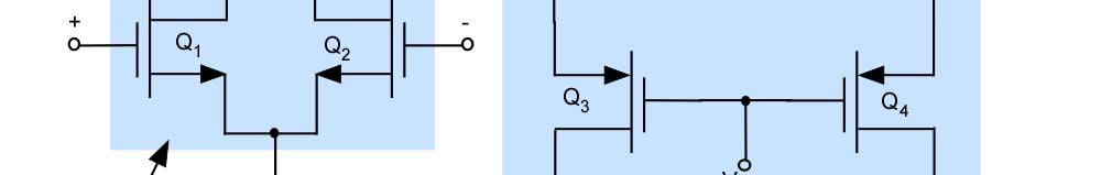
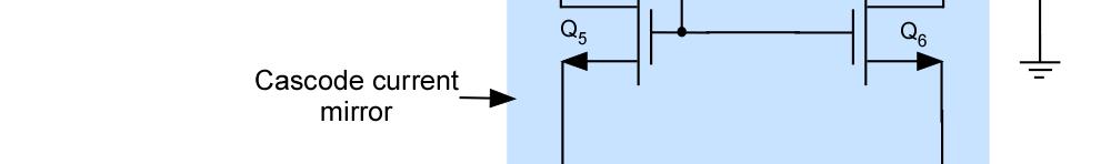
48 741 Op Amp Bias Strategy I REF is generated by mirror Q 11 -Q 12 and R 5 Q 8 -Q 9 current mirror Q 13 double-collector lateral pnp ppdevice; Q 12 and Q 13 form a two-output current mirror Q 13B provides bias current Q 17 Q 13A provides bias current for the output stage Q 18 and Q 19 provide V BE drops to Q 14 and Q 20 48
49 741 Op Amp Input Stage Input Stage Transistors Q 1 through Q 7 make up the input stage Bias is performed by transistors Q 8, Q 9 and Q 10 Q 1 and Q 2 form a differential emitter-follower pair Q 3 and Q 4 form a differential common-base pair Q 5, Q 6 and Q 7 form the load/current mirror to the input stage Q 3 and Q 4 also perform dc level shifting to allow both positive and negative swings 49
50 741 Op Amp Second Stage Second Stage Transistors Q 16, Q 17 and Q 13B make up the intermediate stage Q 16 acts as an emitter follower Q 17 is a common emitter amplifier Output of second stage is at collector of Q 17 Capacitor C C provides Miller compensation Capacitor C C occupies large area in chip 50
51 Amplifier - Class B Operation Class B Amp Arrangement saves power Transistors turn on only when signal is applied npn sources current and pnp sinks current Both transistors are cutoff when v I = 0crossover distortion 51
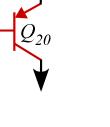
52 741 Op Amp Output Stage Output Stage Class AB operation that reduces crossover distortion Transistors Q 14 and Q 20 make up output t stage Q 18 and Q 19 provide bias to Q 14 and Q 20 52
53 741 Op Amp DC Analysis NPN I A V V 14 : S 10, 200, A 125 PNP I A V V 14 : S 10, 50, A 50 Q 13, Q 14 and Q 20 are nonstandard devices. Q 13 has Q 13A and Q 13B I A, I A SA SB I REF VCC VEB 12 VBE11 ( VEE ) R R ma 53
54 741 Op Amp Input Stage DC Analysis Input Stage Q 11 & Q 10 are a Widlar current source V V I R BE11 BE10 C10 4 ( Assume I S 10 IS 11 ) I V ln REF T IC10R4 I I C10 C10 19 A Transistors Q 1 through Q 4, Q 8 and Q 9 form a negative feedback loop that stabilizes the value of I 54
55 741 Op Amp Input Stage DC Analysis I C 6 I I C5 I 2I V IR 6 2 I 7 7 BE C IE R N 3 V BE 6 VT ln I I S 55
56 741 Op Amp Output Stage DC Bias Output Stage Q 13 delivers a current of 0.25 I REF Class AB operation IC23 IE IREF 180 A I E A I C A IC A 56
57 i e Small-Signal Analysis Input Stage vi 4r e r e is the emitter resistance of Q 1 -Q 4 r e VT 25 mv k I 9.5 A R 4 1 r id N e For N = 200, we obtain R id = 2.1 M 57
58 Small-Signal Analysis Input Stage i o G m1 2 i i v o i e 2r e re 2.63 k 1 Gm1 1/ 5.26 ma/ V 58
59 Small-Signal Analysis Input Stage Output resistance of input stage. Seen from collector of Q 6 1 // R r 1 g R // r o o m E R E =r e =2.63 k and r o =V A /I where V A =50 V and I=9.5 Ar o =5.26 M 59
60 Input Stage Incremental Model Develop equivalent circuit for input stage 60
61 Small-Signal Analysis Second Stage 61
62 Second Stage Incremental Model Develop equivalent circuit for second stage 62


63 Small-Signal Analysis Second Stage Input Resistance R i2 is found by inspection: Ri 1 r e R 1 re R Ri2 4 M 63
64 Small-Signal Analysis Second Stage Transconductance i c17 The transconductance G m2 is the output current to input voltage v vb7 r R e17 8 v v b17 12 R 9// R i 17 R // R r 9 i17 e16 R 1 r R i17 17 e17 8 G m2 i c17 v i ma/ V 64
65 Small-Signal Analysis Second Stage Output Resistance Find resistance looking into into output terminal R R // R o2 o13b o17 First component R r k o13b o13b 90.9 Second component is found looking into collector of Q 17 R 787 k R 2 81 o o k 65
66 Small-Signal Analysis Output Stage Characteristics AB class circuit Driven by Q 17 Q 23 is follower Q 18 & Q 19 providing bias Q 14 & Q 20 are output transistors 66
67 Output Voltage Limits Output Stage Maximum positive voltage limited by saturation of Q 13 v V V V omax CC CEsat BE14 About 1V below V CC Minimum output voltage limited by saturation of Q 17 v V V V V o min EE CEsat EB 23 EB 20 About 1.5 V above -V EE 67
68 Output Stage Incremental Circuit Construct model v G R v o2 m2 o2 i2 G m2 =6.5 ma/v and R o2 =81 k 68
69 Output Stage Incremental Model Finding R in3 Assume Q 20 to have 5 ma Resistance looking into base of Q 20 is about 20 R L Assume 20 =50 and R L =2 kresistance into Q 20 =100 k Q 18 &Q 19 providing bias Place above resistance in parallel with resistance of Q 13A (about 280 k) [resistance of Q 18 -Q 19 network small and can be neglected] Assuming 23 =50 R 100 k // 280 k M in
70 Output Stage Incremental Model Looking into emitter of Q 23 R R r o2 o23 e Using R o2 =81 k, 23 =50, r e23 =25/0.18 = 139 gives R o23 = k R out R o23 re For = 50, R out=34 70
71 Overall Gain vo vi2 vo2 vo vi vi vi2 vo2 vo R L Gm 1 Ro 1// R12 Gm2Ro2 Gvo3 vi RL Rout vo A o ,147 V / V vi v o Ao db v i 71
72 741 Op Amp - Frequency Response Miller capacitance due to C C between the base of Q 16 and ground is C C 1 A in C Resistance between the base of Q 16 and ground is R R // R 6.7 M// 4 M t o1 i2 2 Dominant pole is at Unity gain-bandwith is f P 1 2C R in t 4.1 Hz f A0 f3 243, MHz t db 72
73 Conclusion - Design of Op Amps 1. Designer starts with building blocks whose performance can be analyzed to a first order approximation by hand 2. This step provides insight to the designer as the design of the circuit develops 3. At some point designer must turn to computer analysis programs such as SPICE. This will provide speed and accuracy to the design process 73
ECE 442 Solid State Devices & Circuits. 15. Differential Amplifiers
 ECE 442 Solid State Devices & Circuits 15. Differential Amplifiers Jose E. Schutt-Aine Electrical & Computer Engineering University of Illinois jschutt@emlab.uiuc.edu ECE 442 Jose Schutt Aine 1 Background
Chapter 12 Opertational Amplifier Circuits
 1 Chapter 12 Opertational Amplifier Circuits Learning Objectives 1) The design and analysis of the two basic CMOS op-amp architectures: the two-stage circuit and the single-stage, folded cascode circuit.
ECE 546 Lecture 12 Integrated Circuits
 ECE 546 Lecture 12 Integrated Circuits Spring 2018 Jose E. Schutt-Aine Electrical & Computer Engineering University of Illinois jesa@illinois.edu ECE 546 Jose Schutt Aine 1 Integrated Circuits IC Requirements
Microelectronic Circuits II. Ch 10 : Operational-Amplifier Circuits
 Microelectronic Circuits II Ch 0 : Operational-Amplifier Circuits 0. The Two-stage CMOS Op Amp 0.2 The Folded-Cascode CMOS Op Amp CNU EE 0.- Operational-Amplifier Introduction - Analog ICs : operational
Building Blocks of Integrated-Circuit Amplifiers
 Building Blocks of ntegrated-circuit Amplifiers 1 The Basic Gain Cell CS and CE Amplifiers with Current Source Loads Current-source- or active-loaded CS amplifier Rin A o R A o g r r o g r 0 m o m o Current-source-
Radivoje Đurić, 2015, Analogna Integrisana Kola 1
 OTA-output buffer 1 According to the types of loads, the driving capability of the output stages differs. For switched capacitor circuits which have high impedance capacitive loads, class A output stage
F9 Differential and Multistage Amplifiers
 Lars Ohlsson 018-10-0 F9 Differential and Multistage Amplifiers Outline MOS differential pair Common mode signal operation Differential mode signal operation Large signal operation Small signal operation
EE 140 / EE 240A ANALOG INTEGRATED CIRCUITS FALL 2015 C. Nguyen PROBLEM SET #7
 Issued: Friday, Oct. 16, 2015 PROBLEM SET #7 Due (at 8 a.m.): Monday, Oct. 26, 2015, in the EE 140/240A HW box near 125 Cory. 1. A design error has resulted in a mismatch in the circuit of Fig. PS7-1.
Analog Integrated Circuit Configurations
 Analog Integrated Circuit Configurations Basic stages: differential pairs, current biasing, mirrors, etc. Approximate analysis for initial design MOSFET and Bipolar circuits Basic Current Bias Sources
Chapter 8 Differential and Multistage Amplifiers
 1 Chapter 8 Differential and Multistage Amplifiers Operational Amplifier Circuit Components 2 1. Ch 7: Current Mirrors and Biasing 2. Ch 9: Frequency Response 3. Ch 8: Active-Loaded Differential Pair 4.
Chapter 15 Goals. ac-coupled Amplifiers Example of a Three-Stage Amplifier
 Chapter 15 Goals ac-coupled multistage amplifiers including voltage gain, input and output resistances, and small-signal limitations. dc-coupled multistage amplifiers. Darlington configuration and cascode
Index. Small-Signal Models, 14 saturation current, 3, 5 Transistor Cutoff Frequency, 18 transconductance, 16, 22 transit time, 10
 Index A absolute value, 308 additional pole, 271 analog multiplier, 190 B BiCMOS,107 Bode plot, 266 base-emitter voltage, 16, 50 base-emitter voltages, 296 bias current, 111, 124, 133, 137, 166, 185 bipolar
Advanced Operational Amplifiers
 IsLab Analog Integrated Circuit Design OPA2-47 Advanced Operational Amplifiers כ Kyungpook National University IsLab Analog Integrated Circuit Design OPA2-1 Advanced Current Mirrors and Opamps Two-stage
ECEN 5008: Analog IC Design. Final Exam
 ECEN 5008 Initials: 1/10 ECEN 5008: Analog IC Design Final Exam Spring 2004 Instructions: 1. Exam Policy: Time-limited, 150-minute exam. When the time is called, all work must stop. Put your initials on
BJT Circuits (MCQs of Moderate Complexity)
") BJT Circuits (MCQs of Moderate Complexity) 1. The current ib through base of a silicon npn transistor is 1+0.1 cos (1000πt) ma. At 300K, the rπ in the small signal model of the transistor is i b B C r
BJT Circuits (MCQs of Moderate Complexity) 1. The current ib through base of a silicon npn transistor is 1+0.1 cos (1000πt) ma. At 300K, the rπ in the small signal model of the transistor is i b B C r
Design and Simulation of Low Voltage Operational Amplifier
 Design and Simulation of Low Voltage Operational Amplifier Zach Nelson Department of Electrical Engineering, University of Nevada, Las Vegas 4505 S Maryland Pkwy, Las Vegas, NV 89154 United States of America
What is the typical voltage gain of the basic two stage CMOS opamp we studied? (i) 20dB (ii) 40dB (iii) 80dB (iv) 100dB
 20dB (ii) 40dB (iii) 80dB (iv) 100dB") Department of Electronic ELEC 5808 (ELG 6388) Signal Processing Electronics Final Examination Dec 14th, 2010 5:30PM - 7:30PM R. Mason answer all questions one 8.5 x 11 crib sheets allowed 1. (5 points)
Department of Electronic ELEC 5808 (ELG 6388) Signal Processing Electronics Final Examination Dec 14th, 2010 5:30PM - 7:30PM R. Mason answer all questions one 8.5 x 11 crib sheets allowed 1. (5 points)
Multistage Amplifiers
 Multistage Amplifiers Single-stage transistor amplifiers are inadequate for meeting most design requirements for any of the four amplifier types (voltage, current, transconductance, and transresistance.)
TWO AND ONE STAGES OTA
 TWO AND ONE STAGES OTA F. Maloberti Department of Electronics Integrated Microsystem Group University of Pavia, 7100 Pavia, Italy franco@ele.unipv.it tel. +39-38-50505; fax. +39-038-505677 474 EE Department
UNIT-1 Bipolar Junction Transistors. Text Book:, Microelectronic Circuits 6 ed., by Sedra and Smith, Oxford Press
 UNIT-1 Bipolar Junction Transistors Text Book:, Microelectronic Circuits 6 ed., by Sedra and Smith, Oxford Press Figure 6.1 A simplified structure of the npn transistor. Microelectronic Circuits, Sixth
Lecture 34: Designing amplifiers, biasing, frequency response. Context
 Lecture 34: Designing amplifiers, biasing, frequency response Prof J. S. Smith Context We will figure out more of the design parameters for the amplifier we looked at in the last lecture, and then we will
Lecture 13. Biasing and Loading Single Stage FET Amplifiers. The Building Blocks of Analog Circuits - III
 Lecture 3 Biasing and Loading Single Stage FET Amplifiers The Building Blocks of Analog Circuits III In this lecture you will learn: Current biasing of circuits Current sources and sinks for CS, CG, and
Operational Amplifiers
 CHAPTER 9 Operational Amplifiers Analog IC Analysis and Design 9- Chih-Cheng Hsieh Outline. General Consideration. One-Stage Op Amps / Two-Stage Op Amps 3. Gain Boosting 4. Common-Mode Feedback 5. Input
UNIT I BIASING OF DISCRETE BJT AND MOSFET PART A
 UNIT I BIASING OF DISCRETE BJT AND MOSFET PART A 1. Why do we choose Q point at the center of the load line? 2. Name the two techniques used in the stability of the q point.explain. 3. Give the expression
Chapter 7 Building Blocks of Integrated Circuit Amplifiers: Part D: Advanced Current Mirrors
 1 Chapter 7 Building Blocks of Integrated Circuit Amplifiers: Part D: Advanced Current Mirrors Current Mirror Example 2 Two Stage Op Amp (MOSFET) Current Mirror Example Three Stage 741 Opamp (BJT) 3 4
Chapter 4 Single-stage MOS amplifiers
 Chapter 4 Single-stage MOS amplifiers ELEC-H402/CH4: Single-stage MOS amplifiers 1 Single-stage MOS amplifiers NMOS as an amplifier: example of common-source circuit NMOS amplifier example Introduction
ECE315 / ECE515 Lecture 8 Date:
 ECE35 / ECE55 Lecture 8 Date: 05.09.06 CS Amplifier with Constant Current Source Current Steering Circuits CS Stage Followed by CG Stage Cascode as Current Source Cascode as Amplifier ECE35 / ECE55 CS
LECTURE 19 DIFFERENTIAL AMPLIFIER
 Lecture 19 Differential Amplifier (6/4/14) Page 191 LECTURE 19 DIFFERENTIAL AMPLIFIER LECTURE ORGANIZATION Outline Characterization of a differential amplifier Differential amplifier with a current mirror
CHAPTER 8 DIFFERENTIAL AND MULTISTAGE AMPLIFIERS
 CHAPTER 8 DIFFERENTIAL AND MULTISTAGE AMPLIFIERS Chapter Outline 8.1 The CMOS Differential Pair 8. Small-Signal Operations of the MOS Differential Pair 8.3 The BJT Differential Pair 8.4 Other Non-ideal
d. Can you find intrinsic gain more easily by examining the equation for current? Explain.
 EECS140 Final Spring 2017 Name SID 1. [8] In a vacuum tube, the plate (or anode) current is a function of the plate voltage (output) and the grid voltage (input). I P = k(v P + µv G ) 3/2 where µ is a
Lecture 030 ECE4430 Review III (1/9/04) Page 030-1
 Page 030-1") Lecture 030 ECE4430 Review III (1/9/04) Page 0301 LECTURE 030 ECE 4430 REVIEW III (READING: GHLM Chaps. 3 and 4) Objective The objective of this presentation is: 1.) Identify the prerequisite material
Lecture 030 ECE4430 Review III (1/9/04) Page 0301 LECTURE 030 ECE 4430 REVIEW III (READING: GHLM Chaps. 3 and 4) Objective The objective of this presentation is: 1.) Identify the prerequisite material
55:041 Electronic Circuits
 55:041 Electronic Circuits MOSFETs Sections of Chapter 3 &4 A. Kruger MOSFETs, Page-1 Basic Structure of MOS Capacitor Sect. 3.1 Width = 1 10-6 m or less Thickness = 50 10-9 m or less ` MOS Metal-Oxide-Semiconductor
ANALYSIS AND DESIGN OF ANALOG INTEGRATED CIRCUITS
 ANALYSIS AND DESIGN OF ANALOG INTEGRATED CIRCUITS Fourth Edition PAUL R. GRAY University of California, Berkeley PAUL J. HURST University of California, Davis STEPHEN H. LEWIS University of California,
Unit 3: Integrated-circuit amplifiers (contd.)
") Unit 3: Integrated-circuit amplifiers (contd.) COMMON-SOURCE AND COMMON-EMITTER AMPLIFIERS The Common-Source Circuit The most basic IC MOS amplifier is shown in fig.(1). The source of MOS transistor is
Unit 3: Integrated-circuit amplifiers (contd.) COMMON-SOURCE AND COMMON-EMITTER AMPLIFIERS The Common-Source Circuit The most basic IC MOS amplifier is shown in fig.(1). The source of MOS transistor is
Lecture 240 Cascode Op Amps (3/28/10) Page 240-1
 Page 240-1") Lecture 240 Cascode Op Amps (3/28/10) Page 2401 LECTURE 240 CASCODE OP AMPS LECTURE ORGANIZATION Outline Lecture Organization Single Stage Cascode Op Amps Two Stage Cascode Op Amps Summary CMOS Analog
Lecture 240 Cascode Op Amps (3/28/10) Page 2401 LECTURE 240 CASCODE OP AMPS LECTURE ORGANIZATION Outline Lecture Organization Single Stage Cascode Op Amps Two Stage Cascode Op Amps Summary CMOS Analog
 Pg: 1 VALLIAMMAI ENGINEERING COLLEGE SRM Nagar, Kattankulathur 603 203 Department of Electronics & Communication Engineering Regulation: 2013 Acadamic Year : 2015 2016 EC6304 Electronic Circuits I Question
Chapter 5. Operational Amplifiers and Source Followers. 5.1 Operational Amplifier
 Chapter 5 Operational Amplifiers and Source Followers 5.1 Operational Amplifier In single ended operation the output is measured with respect to a fixed potential, usually ground, whereas in double-ended
The Differential Amplifier. BJT Differential Pair
 1 The Differential Amplifier Asst. Prof. MONTREE SRPRUCHYANUN, D. Eng. Dept. of Teacher Training in Electrical Engineering, Faculty of Technical Education King Mongkut s nstitute of Technology North Bangkok
Building Blocks of Integrated-Circuit Amplifiers
 CHAPTER 7 Building Blocks of Integrated-Circuit Amplifiers Introduction 7. 493 IC Design Philosophy 7. The Basic Gain Cell 494 495 7.3 The Cascode Amplifier 506 7.4 IC Biasing Current Sources, Current
Analog Integrated Circuit Design Exercise 1
 Analog Integrated Circuit Design Exercise 1 Integrated Electronic Systems Lab Prof. Dr.-Ing. Klaus Hofmann M.Sc. Katrin Hirmer, M.Sc. Sreekesh Lakshminarayanan Status: 21.10.2015 Pre-Assignments The lecture
Class-AB Low-Voltage CMOS Unity-Gain Buffers
 Class-AB Low-Voltage CMOS Unity-Gain Buffers Mariano Jimenez, Antonio Torralba, Ramón G. Carvajal and J. Ramírez-Angulo Abstract Class-AB circuits, which are able to deal with currents several orders of
Radivoje Đurić, 2015, Analogna Integrisana Kola 1
 Low power OTA 1 Two-Stage, Miller Op Amp Operating in Weak Inversion Low frequency response: gm1 gm6 Av 0 g g g g A v 0 ds2 ds4 ds6 ds7 I D m, ds D nvt g g I n GB and SR: GB 1 1 n 1 2 4 6 6 7 g 2 2 m1
Microelectronics Part 2: Basic analog CMOS circuits
 GBM830 Dispositifs Médicaux Intelligents Microelectronics Part : Basic analog CMOS circuits Mohamad Sawan et al. Laboratoire de neurotechnologies Polystim!! http://www.cours.polymtl.ca/gbm830/! mohamad.sawan@polymtl.ca!
Code: 9A Answer any FIVE questions All questions carry equal marks *****
 II B. Tech II Semester (R09) Regular & Supplementary Examinations, April/May 2012 ELECTRONIC CIRCUIT ANALYSIS (Common to EIE, E. Con. E & ECE) Time: 3 hours Max Marks: 70 Answer any FIVE questions All
ECEN 474/704 Lab 6: Differential Pairs
 ECEN 474/704 Lab 6: Differential Pairs Objective Design, simulate and layout various differential pairs used in different types of differential amplifiers such as operational transconductance amplifiers
Current Mirrors. Prof. Tai-Haur Kuo, EE, NCKU, Tainan City, Taiwan 4-1
 Current Mirrors Prof. Tai-Haur Kuo, EE, NCKU, Tainan City, Taiwan 4- 郭泰豪, Analog C Design, 08 { Prof. Tai-Haur Kuo, EE, NCKU, Tainan City, Taiwan 4- 郭泰豪, Analog C Design, 08 { Current Source and Sink Symbol
Lecture 300 Low Voltage Op Amps (3/28/10) Page 300-1
 Page 300-1") Lecture 300 Low Voltage Op Amps (3/28/10) Page 300-1 LECTURE 300 LOW VOLTAGE OP AMPS LECTURE ORGANIZATION Outline Introduction Low voltage input stages Low voltage gain stages Low voltage bias circuits
Lecture 300 Low Voltage Op Amps (3/28/10) Page 300-1 LECTURE 300 LOW VOLTAGE OP AMPS LECTURE ORGANIZATION Outline Introduction Low voltage input stages Low voltage gain stages Low voltage bias circuits
Improving Amplifier Voltage Gain
 15.1 Multistage ac-coupled Amplifiers 1077 TABLE 15.3 Three-Stage Amplifier Summary HAND ANALYSIS SPICE RESULTS Voltage gain 998 1010 Input signal range 92.7 V Input resistance 1 M 1M Output resistance
Preliminary Exam, Fall 2013 Department of Electrical and Computer Engineering University of California, Irvine EECS 170B
 Preliminary Exam, Fall 2013 Department of Electrical and Computer Engineering University of California, Irvine EECS 170B Problem 1. Consider the following circuit, where a saw-tooth voltage is applied
QUESTION BANK for Analog Electronics 4EC111 *
 OpenStax-CNX module: m54983 1 QUESTION BANK for Analog Electronics 4EC111 * Bijay_Kumar Sharma This work is produced by OpenStax-CNX and licensed under the Creative Commons Attribution License 4.0 Abstract
d. Why do circuit designers like to use feedback when they make amplifiers? Give at least two reasons.
 EECS105 Final 5/12/10 Name SID 1 /20 2 /30 3 /20 4 /20 5 /30 6 /40 7 /20 8 /20 Total 1. Give a short answer to each question a. Your friend from Stanford says that he has designed a three-stage high gain
ECEN474: (Analog) VLSI Circuit Design Fall 2011
 VLSI Circuit Design Fall 2011") ECEN474: (Analog) VLSI Circuit Design Fall 20 Lecture 22: Output Stages Sebastian Hoyos Analog & Mixed-Signal Center Texas A&M University Agenda Output Stages Source Follower (Class A) Push-Pull (Class
ECEN474: (Analog) VLSI Circuit Design Fall 20 Lecture 22: Output Stages Sebastian Hoyos Analog & Mixed-Signal Center Texas A&M University Agenda Output Stages Source Follower (Class A) Push-Pull (Class
Lecture 4: Voltage References
 EE6378 Power Management Circuits Lecture 4: oltage References Instructor: t Prof. Hoi Lee Mixed-Signal & Power IC Laboratory Department of Electrical Engineering The University of Texas at Dallas Introduction
DC Coupling: General Trends
 DC Coupling: General Trends * Goal: want both input and output to be centered at halfway between the positive and negative supplies (or ground, for a single supply) -- in order to have maximum possible
Applied Electronics II
 Applied Electronics II Chapter 2: Differential Amplifier School of Electrical and Computer Engineering Addis Ababa Institute of Technology Addis Ababa University Daniel D./Abel G. April 4, 2016 Chapter
55:041 Electronic Circuits
 55:041 Electronic Circuits Mosfet Review Sections of Chapter 3 &4 A. Kruger Mosfet Review, Page-1 Basic Structure of MOS Capacitor Sect. 3.1 Width 1 10-6 m or less Thickness 50 10-9 m or less ` MOS Metal-Oxide-Semiconductor
University of Michigan, EECS413 Final project. A High Speed Operational Amplifier. 1. A High Speed Operational Amplifier
 University of Michigan, EECS413 Final project. A High Speed Operational Amplifier. 1 A High Speed Operational Amplifier A. Halim El-Saadi, Mohammed El-Tanani, University of Michigan Abstract This paper
Reading. Lecture 33: Context. Lecture Outline. Chapter 9, multi-stage amplifiers. Prof. J. S. Smith
 eading Lecture 33: Chapter 9, multi-stage amplifiers Prof J. S. Smith Context Lecture Outline We are continuing to review some of the building blocks for multi-stage amplifiers, including current sources
HOME ASSIGNMENT. Figure.Q3
 HOME ASSIGNMENT 1. For the differential amplifier circuit shown below in figure.q1, let I=1 ma, V CC =5V, v CM = -2V, R C =3kΩ and β=100. Assume that the BJTs have v BE =0.7 V at i C =1 ma. Find the voltage
A 16Ω Audio Amplifier with 93.8 mw Peak loadpower and 1.43 quiscent power consumption
 A 16Ω Audio Amplifier with 93.8 mw Peak loadpower and 1.43 quiscent power consumption IEEE Transactions on circuits and systems- Vol 59 No:3 March 2012 Abstract A class AB audio amplifier is used to drive
4. Differential Amplifiers. Electronic Circuits. Prof. Dr. Qiuting Huang Integrated Systems Laboratory
 4. Differential Amplifiers Electronic Circuits Prof. Dr. Qiuting Huang Integrated Systems Laboratory Differential Signaling Basics and Motivation Transmitting information with two complementary signals
Experiment #7 MOSFET Dynamic Circuits II
 Experiment #7 MOSFET Dynamic Circuits II Jonathan Roderick Introduction The previous experiment introduced the canonic cells for MOSFETs. The small signal model was presented and was used to discuss the
Rail-To-Rail Output Op-Amp Design with Negative Miller Capacitance Compensation
 Rail-To-Rail Op-Amp Design with Negative Miller Capacitance Compensation Muhaned Zaidi, Ian Grout, Abu Khari bin A ain Abstract In this paper, a two-stage op-amp design is considered using both Miller
55:041 Electronic Circuits The University of Iowa Fall Exam 3. Question 1 Unless stated otherwise, each question below is 1 point.
 Exam 3 Name: Score /65 Question 1 Unless stated otherwise, each question below is 1 point. 1. An engineer designs a class-ab amplifier to deliver 2 W (sinusoidal) signal power to an resistive load. Ignoring
Analysis and Design of Analog Integrated Circuits Lecture 18. Key Opamp Specifications
 Analysis and Design of Analog Integrated Circuits Lecture 8 Key Opamp Specifications Michael H. Perrott April 8, 0 Copyright 0 by Michael H. Perrott All rights reserved. Recall: Key Specifications of Opamps
SAMPLE FINAL EXAMINATION FALL TERM
 ENGINEERING SCIENCES 154 ELECTRONIC DEVICES AND CIRCUITS SAMPLE FINAL EXAMINATION FALL TERM 2001-2002 NAME Some Possible Solutions a. Please answer all of the questions in the spaces provided. If you need
ANALYSIS AND DESIGN OF ANALOG INTEGRATED CIRCUITS
 ANALYSIS AND DESIGN OF ANALOG INTEGRATED CIRCUITS Fourth Edition PAUL R. GRAY University of California, Berkeley PAUL J. HURST University of California, Davis STEPHEN H. LEWIS University of California,
EE LINEAR INTEGRATED CIRCUITS & APPLICATIONS
 UNITII CHARACTERISTICS OF OPAMP 1. What is an opamp? List its functions. The opamp is a multi terminal device, which internally is quite complex. It is a direct coupled high gain amplifier consisting of
Course Number Section. Electronics I ELEC 311 BB Examination Date Time # of pages. Final August 12, 2005 Three hours 3 Instructor
 Course Number Section Electronics ELEC 311 BB Examination Date Time # of pages Final August 12, 2005 Three hours 3 nstructor Dr. R. Raut M aterials allowed: No Yes X (Please specify) Calculators allowed:
CSE 577 Spring Insoo Kim, Kyusun Choi Mixed Signal CHIP Design Lab. Department of Computer Science & Engineering The Penn State University
 CSE 577 Spring 2011 Basic Amplifiers and Differential Amplifier, Kyusun Choi Mixed Signal CHIP Design Lab. Department of Computer Science & Engineering The Penn State University Don t let the computer
Advanced OPAMP Design
 Advanced OPAMP Design Two Stage OPAMP with Cascoding To increase the gain, the idea of cascoding can be combined with the idea of cascading. A two stage amplifier with one stage being cascode is possible.
Lecture 33: Context. Prof. J. S. Smith
 Lecture 33: Prof J. S. Smith Context We are continuing to review some of the building blocks for multi-stage amplifiers, including current sources and cascode connected devices, and we will also look at
Differential Amplifier Design
 Differential Amplifier Design Design with ideal current source bias. Differential and common mode gain results Add finite output resistance to current source. Replace ideal current source with current
Operational Amplifier (OPAMP)
") Operational Amplifier (OPAMP) Analog Cs nclude Operational Amplifier Filters Analog-to-Digital Converter (ADC) Digital-to-Analog Converter (DAC) Analog Modulator Phase-Locked Loop Analog Multiplier Others
Operational Amplifier (OPAMP) Analog Cs nclude Operational Amplifier Filters Analog-to-Digital Converter (ADC) Digital-to-Analog Converter (DAC) Analog Modulator Phase-Locked Loop Analog Multiplier Others
NJM324C. Low power quad operational amplifiers
 Low power quad operational amplifiers Features Wide gain bandwidth:.mhz typ. Input common-mode voltage range includes ground Large voltage gain:db typ. Very low supply current per amplifier:ua typ. Low
Chapter 13 Output Stages and Power Amplifiers
 Chapter 13 Output Stages and Power Amplifiers 13.1 General Considerations 13.2 Emitter Follower as Power Amplifier 13.3 Push-Pull Stage 13.4 Improved Push-Pull Stage 13.5 Large-Signal Considerations 13.6
The Miller Approximation. CE Frequency Response. The exact analysis is worked out on pp of H&S.
 CE Frequency Response The exact analysis is worked out on pp. 639-64 of H&S. The Miller Approximation Therefore, we consider the effect of C µ on the input node only V ---------- out V s = r g π m ------------------
Common mode rejection ratio
 Common mode rejection ratio Definition: Common mode rejection ratio represents the ratio of the differential voltage gaina d tothecommonmodevoltagegain,a cm : Common mode rejection ratio Definition: Common
Lecture 21: Voltage/Current Buffer Freq Response
 Lecture 21: Voltage/Current Buffer Freq Response Prof. Niknejad Lecture Outline Last Time: Frequency Response of Voltage Buffer Frequency Response of Current Buffer Current Mirrors Biasing Schemes Detailed
Homework Assignment EE 435 Homework 4 Spring 2014 Due Wednesday Feb 26
 Homework Assignment EE 435 Homework 4 Spring 2014 Due Wednesday Feb 26 In the following problems, if reference to a semiconductor process is needed, assume processes with the following characteristics:
Field Effect Transistors
 Field Effect Transistors LECTURE NO. - 41 Field Effect Transistors www.mycsvtunotes.in JFET MOSFET CMOS Field Effect transistors - FETs First, why are we using still another transistor? BJTs had a small
COMPARISON OF THE MOSFET AND THE BJT:
 COMPARISON OF THE MOSFET AND THE BJT: In this section we present a comparison of the characteristics of the two major electronic devices: the MOSFET and the BJT. To facilitate this comparison, typical
ECE 415/515 ANALOG INTEGRATED CIRCUIT DESIGN
 ECE 415/515 ANALOG INTEGRATED CIRCUIT DESIGN OPAMP DESIGN AND SIMULATION Vishal Saxena OPAMP DESIGN PROJECT R 2 v out v in /2 R 1 C L v in v out V CM R L V CM C L V CM -v in /2 R 1 C L (a) (b) R 2 ECE415/EO
Basic Circuits. Current Mirror, Gain stage, Source Follower, Cascode, Differential Pair,
 Basic Circuits Current Mirror, Gain stage, Source Follower, Cascode, Differential Pair, CCS - Basic Circuits P. Fischer, ZITI, Uni Heidelberg, Seite 1 Reminder: Effect of Transistor Sizes Very crude classification:
Basic OpAmp Design and Compensation. Chapter 6
 Basic OpAmp Design and Compensation Chapter 6 6.1 OpAmp applications Typical applications of OpAmps in analog integrated circuits: (a) Amplification and filtering (b) Biasing and regulation (c) Switched-capacitor
ECE 363 FINAL (F16) 6 problems for 100 pts Problem #1: Fuel Pump Controller (18 pts)
 6 problems for 100 pts Problem #1: Fuel Pump Controller (18 pts)") ECE 363 FINAL (F16) NAME: 6 problems for 100 pts Problem #1: Fuel Pump Controller (18 pts) You are asked to design a high-side switch for a remotely operated fuel pump. You decide to use the IRF9520 power
ECE 363 FINAL (F16) NAME: 6 problems for 100 pts Problem #1: Fuel Pump Controller (18 pts) You are asked to design a high-side switch for a remotely operated fuel pump. You decide to use the IRF9520 power
Lecture 20 Transistor Amplifiers (II) Other Amplifier Stages. November 17, 2005
 Other Amplifier Stages. November 17, 2005") 6.012 Microelectronic Devices and Circuits Fall 2005 Lecture 20 1 Lecture 20 Transistor Amplifiers (II) Other Amplifier Stages November 17, 2005 Contents: 1. Common source amplifier (cont.) 2. Common drain
6.012 Microelectronic Devices and Circuits Fall 2005 Lecture 20 1 Lecture 20 Transistor Amplifiers (II) Other Amplifier Stages November 17, 2005 Contents: 1. Common source amplifier (cont.) 2. Common drain
BJT Amplifier. Superposition principle (linear amplifier)
") BJT Amplifier Two types analysis DC analysis Applied DC voltage source AC analysis Time varying signal source Superposition principle (linear amplifier) The response of a linear amplifier circuit excited
BJT Amplifier Two types analysis DC analysis Applied DC voltage source AC analysis Time varying signal source Superposition principle (linear amplifier) The response of a linear amplifier circuit excited
Unit- I- Biasing Of Discrete BJT and MOSFET
 Part- A QUESTIONS: Unit- I- Biasing Of Discrete BJT and MOSFET 1. Describe about BJT? BJT consists of 2 PN junctions. It has three terminals: emitter, base and collector. Transistor can be operated in
*For stability of the feedback loop, the differential gain must vary as. / ), e.g. a single-pole rolloff with unity gain at. The unity-gain frequency
, e.g. a single-pole rolloff with unity gain at. The unity-gain frequency") ECE137a Lab project 3 You must purchase lead-free solder from the electronics shop. Do not purchase solder elsewhere, as it will likely be tin/lead solder, which is toxic. "Solder-sucker" desoldering tools
ECE137a Lab project 3 You must purchase lead-free solder from the electronics shop. Do not purchase solder elsewhere, as it will likely be tin/lead solder, which is toxic. "Solder-sucker" desoldering tools
GATE: Electronics MCQs (Practice Test 1 of 13)
") GATE: Electronics MCQs (Practice Test 1 of 13) 1. Removing bypass capacitor across the emitter leg resistor in a CE amplifier causes a. increase in current gain b. decrease in current gain c. increase
GATE: Electronics MCQs (Practice Test 1 of 13) 1. Removing bypass capacitor across the emitter leg resistor in a CE amplifier causes a. increase in current gain b. decrease in current gain c. increase
Lab 2: Discrete BJT Op-Amps (Part I)
") Lab 2: Discrete BJT Op-Amps (Part I) This is a three-week laboratory. You are required to write only one lab report for all parts of this experiment. 1.0. INTRODUCTION In this lab, we will introduce and
Lab 2: Discrete BJT Op-Amps (Part I) This is a three-week laboratory. You are required to write only one lab report for all parts of this experiment. 1.0. INTRODUCTION In this lab, we will introduce and
Lecture 14. FET Current and Voltage Sources and Current Mirrors. The Building Blocks of Analog Circuits - IV
 Lecture 4 FET Current and oltage s and Current Mirrors The Building Blocks of Analog Circuits n this lecture you will learn: Current and voltage sources using FETs FET current mirrors Cascode current mirror
ECEN 474/704 Lab 5: Frequency Response of Inverting Amplifiers
 ECEN 474/704 Lab 5: Frequency Response of Inverting Amplifiers Objective Design, simulate and layout various inverting amplifiers. Introduction Inverting amplifiers are fundamental building blocks of electronic
Homework Assignment 12
 Homework Assignment 12 Question 1 Shown the is Bode plot of the magnitude of the gain transfer function of a constant GBP amplifier. By how much will the amplifier delay a sine wave with the following
Low-Power Quad Operational Amplifier FEATURES: DESCRIPTION: Memory. Logic Diagram. RAD-PAK technology-hardened against natural space radiation
 Low-Power Quad Operational Amplifier FEATURES: RAD-PAK technology-hardened against natural space radiation Total dose hardness: - > 100 krad (Si), depending upon space mission Excellent Single Event Effects:
Dual Channel PWM Controller with SCP / DTC Function
 Dual Channel PWM Controller with SCP / DTC Function General Description The FP545A is a dual channel PWM buck controller with short circuit protection (SCP) and adjustable maximum duty control (DTC) function.
A CMOS Low-Voltage, High-Gain Op-Amp
 A CMOS Low-Voltage, High-Gain Op-Amp G N Lu and G Sou LEAM, Université Pierre et Marie Curie Case 203, 4 place Jussieu, 75252 Paris Cedex 05, France Telephone: (33 1) 44 27 75 11 Fax: (33 1) 44 27 48 37
V o. ECE2280 Homework #1 Fall Use: ignore r o, V BE =0.7, β=100 V I = sin(20t) For DC analysis, assume that the capacitors are open
 For DC analysis, assume that the capacitors are open") ECE2280 Homework #1 Fall 2011 1. Use: ignore r o, V BE =0.7, β=100 V I = 200.001sin(20t) For DC analysis, assume that the capacitors are open (a) Solve for the DC currents: a. I B b. I E c. I C (b) Solve
ECE2280 Homework #1 Fall 2011 1. Use: ignore r o, V BE =0.7, β=100 V I = 200.001sin(20t) For DC analysis, assume that the capacitors are open (a) Solve for the DC currents: a. I B b. I E c. I C (b) Solve
ECE 255, MOSFET Amplifiers
 ECE 255, MOSFET Amplifiers 26 October 2017 In this lecture, the basic configurations of MOSFET amplifiers will be studied similar to that of BJT. Previously, it has been shown that with the transistor