ECE 415/515 ANALOG INTEGRATED CIRCUIT DESIGN
|
|
|
- Christopher Clarke
- 5 years ago
- Views:
Transcription

1 ECE 415/515 ANALOG INTEGRATED CIRCUIT DESIGN OPAMP DESIGN AND SIMULATION Vishal Saxena
2 OPAMP DESIGN PROJECT R 2 v out v in /2 R 1 C L v in v out V CM R L V CM C L V CM -v in /2 R 1 C L (a) (b) R 2 ECE415/EO ECE515
3 DESIGN SPECIFICATIONS
4 TWO-STAGE OPAMP
5 TWO-STAGE OPAMP: MILLER COMPENSATION
6 MILLER COMPENSATION EQUATIONS
7 TWO-STAGE OPAMP: ZERO-NULLING R
8 VOLTAGE BUFFER COMPENSATION
9 COMMON-GATE COMPENSATION
10 CLASS-A STAGE: SLEWING
11 CLASS-AB STAGE: FLOATING MIRROR
12 TELESCOPIC+CLASS-AB STAGE V bias2 V bias5 Note that in this schematic, Indirect compensation is used. Cc is connected between v out and an internal lowimpedance node For Miller compensation, connect Cc between nodes 1 and 2. V bias5 is generated using a replica bias circuit
13 FOLDED-CASCODE STAGE
14 FOLDED-CASCODE WITH CLASS-AB OUTPUT Note that in this schematic, Indirect compensation is used. Cc is connected between v out and an internal lowimpedance node For Miller compensation, connect Cc between nodes 1 and 2.
15 FC+CLASS-AB+RAIL-TO-RAIL INPUT
16 GAIN ENHANCEMENT Note that in this schematic, Indirect compensation is used. Cc is connected between v out and an internal lowimpedance node For Miller compensation, connect Cc between nodes 1 and 2.
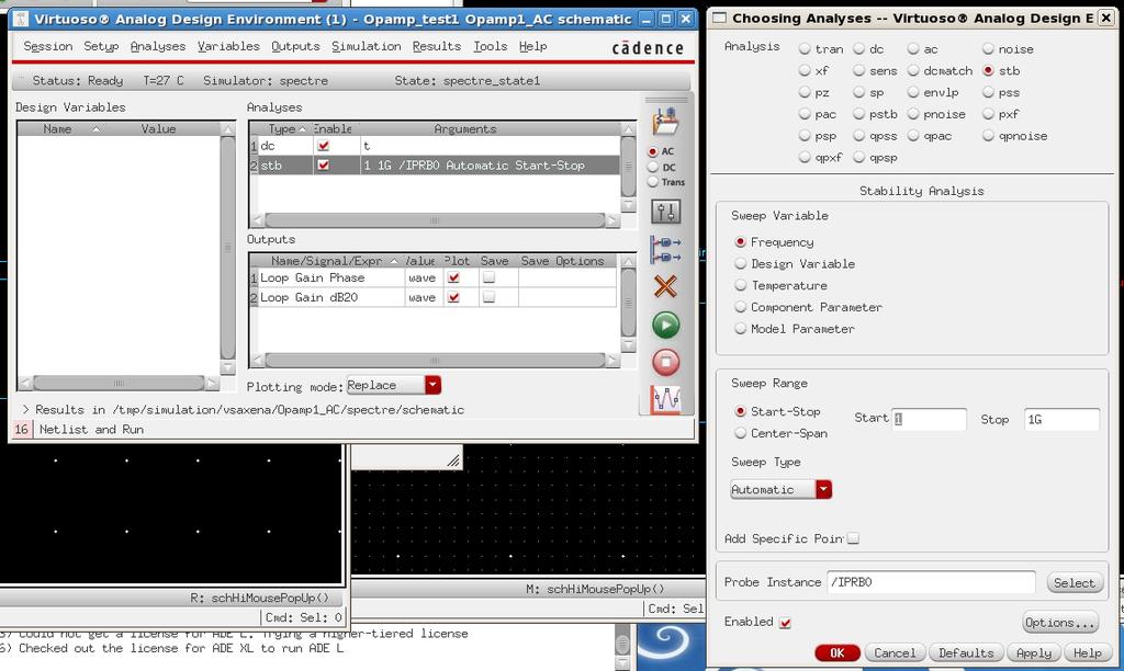
17 CADENCE SPECTRE STB ANALYSIS
18 SPECTRE STB ANALYSIS The STB analysis linearizes the circuit about the DC operating point and computes the loop-gain, gain and phase margins (if the sweep variable is frequency), for a feedback loop or a gain device [1]. Refer to the Spectre Simulation Refrence [1] and [2] for details.

19 EXAMPLE SINGLE-ENDED OPAMP SCHEMATIC
 the")
20 STB ANALYSIS TEST BENCH Pay attention to the iprobe component (from analoglib) Acts as a short for DC, but breaks the loop in stb analysis Place the probe at a point where it completely breaks (all) the loop(s).

21 DC ANNOTATION Annotating the node voltages and DC operating points of the devices helps debug the design Check device gds to see if its in triode or saturation regions
22 SIMULATION SETUP

23 BODE PLOT SETUP Results->Direct Plot-> Main Form
24 OPEN-LOOP RESPONSE (BODE PLOTS) Here, f un =152.5 MHz, PM=41.8 Best to use the stb analysis with circuit is in the desired feedback configuration Break the loop with realistic DC operation points
 Compensate more ( Cc and/or g m2")
25 SMALL STEP RESPONSE 10mV Observe the ringing (PM was 41 ) Compensate more ( Cc and/or g m2 )

26 LARGE STEP RESPONSE 500mV Note the slewing in the output Class-A: I 2 /C L Class-AB: I SS /C C
27 XF ANALYSIS (FOR CMRR, PSRR) For CMRR and PSRR plots, you can use xf analysis. Set up your testbench sources for the supplies (of course), but also a source representing the common mode voltage. Then run an xf analysis and tell it where the output of the circuit. You can then plot the transfer function from every source to the differential output of the circuit.

28 XF ANALYSIS XF analysis simultaneously computes individual transfer functions from every independent source to a single output.

29 TWO-STAGE OPAMP COMPENSATION TECHNIQUES
30 MILLER COMPENSATION VDD M3 v m v i p C fb M1 M2 v out M6TL M6BL V bias3 V bias4 Unlabeled NMOS are 10/2. Unlabeled PMOS are 22/2. VDD M4 M6TR M6BR 1 750Ω i C ff C C M8T M8B VDD M7 10pF x10 220/ /2 100/2 C L 30pF Compensation capacitor (C c ) between the output of the gain stages causes pole-splitting and achieves dominant pole compensation. An RHP zero exists at Due to feed-forward component of the compensation current (i C ). The second pole is located at The unity-gain frequency is A benign undershoot in step-response due to the RHP zero All the op-amps presented have been designed in AMI C5N 0.5μm CMOS process with scale=0.3 μm and L min =2. The op-amps drive a 30pF off-chip load offered by the test-setup.
31 DRAWBACKS OF MILLER COMPENSATION VDD M3 v m v p vout M6TL M6BL M1 V bias3 V bias4 Unlabeled NMOS are 10/2. Unlabeled PMOS are 22/2. VDD M2 M4 M6TR M6BR 1 C C 10pF M8T M8B VDD M7 x10 220/ /2 100/2 C L 30pF The RHP zero decreases phase margin Requires large C C for compensation (10pF here for a 30pF load!). Slow-speed for a given load, C L. Poor PSRR Supply noise feeds to the output through C C. Large layout size.
32 v m v p INDIRECT (AHUJA) COMPENSATION VDD M3 M6TL M6BL M1 V bias3 V bias4 M6TR M6BR Unlabeled NMOS are 10/2. Unlabeled PMOS are 22/2. VDD M2 M4 M10T M10B M CG VDD M9 A i c 1 C c M8T M8B VDD x10 M7 220/ /2 100/2 An indirect-compensated op-amp using a common-gate stage. v out C L 30pF The RHP zero can be eliminated by blocking the feed-forward compensation current component by using A common gate stage, A voltage buffer, Common gate embedded in the cascode diffamp, or A current mirror buffer. Now, the compensation current is fed-back from the output to node-1 indirectly through a low-z node-a. Since node-1 is not loaded by C C, this results in higher unity-gain frequency (f un ).
33 INDIRECT (CASCODE) COMPENSATION VDD M3T M3B M4B V bias2 v m v p vout M6TL M6BL M1 V bias3 V bias4 M4T Unlabeled NMOS are 10/2. Unlabeled PMOS are 44/2. VDD M2 A 1 M6TR M6BR i c C C M7 1.5pF M8T M8B VDD 110/2 2 50/2 50/2 C L 30pF Indirect-compensation using cascoded current mirror load. VDD M3 M1T v out A v m v p 1.5pF 2 M1B M2B V bias3 M5T V bias4 M5B V bias5 30/2 30/2 Unlabeled NMOS are 10/2. Unlabeled PMOS are 22/2. VDD 1 M4 M2T i c C C M7 M8T M8B VDD 220/2 100/2 100/2 C L 30pF Indirect-compensation using cascoded diff-pair. Employing the common gate device embedded in the cascode structure for indirect compensation avoids a separate buffer stage. Lower power consumption. Also voltage buffer reduces the swing which is avoided here.
34 Small signal analytical model INDIRECT COMPENSATION: MODELING C c + - v in R c A A 1 A 2 Differential Amplifier i c 1 2 Gain Stage Block Diagram v out v i out c 1 sc c R 1 c 2 g m1 v s R 1 C 1 g m2 v 1 R 2 C 2 v out C c R c The compensation current (i C ) is indirectly fed-back to node R C is the resistance attached to node-a.
35 Resistance r oc is assumed to be large. g mc >>r oc -1, R A -1, C C >>C A The small-signal model for a common gate indirect compensated opamp topology is approximated to the simplified model seen in the last slide.
36 INDIRECT COMPENSATION: EQUATIONS j un p 3 p 2 z 1 p 1 LHP zero Pole p 2 is much farther away from f un. Can use smaller g m2 =>less power! LHP zero improves phase margin. Much faster op-amp with lower power and smaller C C. Better slew rate as C C is smaller.
37 Amplitude Phase (deg) Magnitude (db) EFFECT OF LHP ZERO ON SETTLING In certain cases with indirect compensation, the LHP-zero (ω z,lhp ) shows up near f un. Causes gain flattening and degrades PM Hard to push out due to topology restrictions Ringing in closed-loop step response Used to be a benign undershoot with the RHP zero, here it can be pesky Is this settling behavior acceptable? Watch out for the ω z,lhp for clean settling behavior! When using indirect compensation be aware of the LHP-zero induced transient settling issues Bode Diagram Frequency (Hz) Closed Loop Step Response Time (sec) Small step-input settling in follower configuration x 10-7
38 REFERENCES 1. The Designer s Guide to SPICE and Spectre: 2. Spectre User Simulation Guide, pages : 3. M. Tian, V. Viswanathan, J. Hangtan, K. Kundert, Striving for Small-Signal Stability: Loop-based and Device-based Algorithms for Stability Analysis of Linear Analog Circuits in the Frequency Domain, Circuits and Devices, Jan Saxena V, Baker R.J., Indirect feedback compensation of CMOS op-amps, IEEE WMED 2006.
39 REFERENCES 6. Saxena V, Baker R.J., Indirect compensation techniques for three-stage CMOS op-amps, IEEE MWSCAS Saxena V., Baker R.J., Indirect compensation techniques for three-stage fully-differential op-amps, IEEE MWSCAS Saxena V. Indirect Feedback Compensation Technique for Multi-Stage Operational Amplifiers, MS Thesis, Boise State University, 2007.
Design of High-Speed Op-Amps for Signal Processing
 Design of High-Speed Op-Amps for Signal Processing R. Jacob (Jake) Baker, PhD, PE Professor and Chair Boise State University 1910 University Dr. Boise, ID 83725-2075 jbaker@ieee.org Abstract - As CMOS
Topology Selection: Input
 Project #2: Design of an Operational Amplifier By: Adrian Ildefonso Nedeljko Karaulac I have neither given nor received any unauthorized assistance on this project. Process: Baker s 50nm CAD Tool: Cadence
Amplifiers Frequency Response Examples
 ECE 5/45 Analog IC Design We will use the following MOSFET parameters for hand-calculations and the µm CMOS models for corresponding simulations. Table : Long-channel MOSFET parameters. Parameter NMOS
Revision History. Contents
 Revision History Ver. # Rev. Date Rev. By Comment 0.0 9/15/2012 Initial draft 1.0 9/16/2012 Remove class A part 2.0 9/17/2012 Comments and problem 2 added 3.0 10/3/2012 cmdmprobe re-simulation, add supplement
Design and Simulation of Low Voltage Operational Amplifier
 Design and Simulation of Low Voltage Operational Amplifier Zach Nelson Department of Electrical Engineering, University of Nevada, Las Vegas 4505 S Maryland Pkwy, Las Vegas, NV 89154 United States of America
Common Mode Feedback for Fully Differential Amplifier in ami06 micron CMOS process
 Published by : http:// Common Mode Feedback for Fully Differential Amplifier in ami06 micron CMOS process Ravi Teja Bojanapally Department of Electrical and Computer Engineering, Texas Tech University,
Low Power and Fast Transient High Swing CMOS Telescopic Operational Amplifier
 RESEARCH ARTICLE OPEN ACCESS Low Power and Fast Transient High Swing CMOS Telescopic Operational Amplifier Akshay Kumar Kansal 1, Asst Prof. Gayatri Sakya 2 Electronics and Communication Department, 1,2
Design Analysis and Performance Comparison of Low Power High Gain 2nd Stage Differential Amplifier Along with 1st Stage
 Design Analysis and Performance Comparison of Low Power High Gain 2nd Stage Differential Amplifier Along with 1st Stage Sadeque Reza Khan Department of Electronic and Communication Engineering, National
Advanced Operational Amplifiers
 IsLab Analog Integrated Circuit Design OPA2-47 Advanced Operational Amplifiers כ Kyungpook National University IsLab Analog Integrated Circuit Design OPA2-1 Advanced Current Mirrors and Opamps Two-stage
High bandwidth low power operational amplifier design and compensation techniques
 Graduate Theses and Dissertations Graduate College 2009 High bandwidth low power operational amplifier design and compensation techniques Vaibhav Kumar Iowa State University Follow this and additional
Operational Amplifier with Two-Stage Gain-Boost
 Proceedings of the 6th WSEAS International Conference on Simulation, Modelling and Optimization, Lisbon, Portugal, September 22-24, 2006 482 Operational Amplifier with Two-Stage Gain-Boost FRANZ SCHLÖGL
EECE488: Analog CMOS Integrated Circuit Design Set 7 Opamp Design
 EECE488: Analog CMOS Integrated Circuit Design Set 7 Opamp Design References: Analog Integrated Circuit Design by D. Johns and K. Martin and Design of Analog CMOS Integrated Circuits by B. Razavi All figures
PURPOSE: NOTE: Be sure to record ALL results in your laboratory notebook.
 EE4902 Lab 9 CMOS OP-AMP PURPOSE: The purpose of this lab is to measure the closed-loop performance of an op-amp designed from individual MOSFETs. This op-amp, shown in Fig. 9-1, combines all of the major
Design and Analysis of Low Power Two Stage CMOS Op- Amp with 50nm Technology
 Design and Analysis of Low Power Two Stage CMOS Op- Amp with 50nm Technology Swetha Velicheti, Y. Sandhyarani, P.Praveen kumar, B.Umamaheshrao Assistant Professor, Dept. of ECE, SSCE, Srikakulam, A.P.,
Chapter 12 Opertational Amplifier Circuits
 1 Chapter 12 Opertational Amplifier Circuits Learning Objectives 1) The design and analysis of the two basic CMOS op-amp architectures: the two-stage circuit and the single-stage, folded cascode circuit.
Comparative Analysis of Compensation Techniques for improving PSRR of an OPAMP
 Comparative Analysis of Compensation Techniques for improving PSRR of an OPAMP 1 Pathak Jay, 2 Sanjay Kumar M.Tech VLSI and Embedded System Design, Department of School of Electronics, KIIT University,
Performance Analysis of Low Power, High Gain Operational Amplifier Using CMOS VLSI Design
 RESEARCH ARTICLE OPEN ACCESS Performance Analysis of Low Power, High Gain Operational Amplifier Using CMOS VLSI Design Ankush S. Patharkar*, Dr. Shirish M. Deshmukh** *(Department of Electronics and Telecommunication,
EE 501 Lab 11 Common mode feedback (CMFB) circuit
 circuit") EE 501 Lab 11 Common mode feedback (CMFB) circuit Objectives: Report due: November 17, 2016 1. Understand why CMFB circuits are needed and how they work to ensure robust operation. 2. Understand the advantages
EE 501 Lab 11 Common mode feedback (CMFB) circuit Objectives: Report due: November 17, 2016 1. Understand why CMFB circuits are needed and how they work to ensure robust operation. 2. Understand the advantages
Nonlinear Macromodeling of Amplifiers and Applications to Filter Design.
 ECEN 622 Nonlinear Macromodeling of Amplifiers and Applications to Filter Design. By Edgar Sanchez-Sinencio Thanks to Heng Zhang for part of the material OP AMP MACROMODELS Systems containing a significant
DESIGN OF A FULLY DIFFERENTIAL HIGH-SPEED HIGH-PRECISION AMPLIFIER
 DESIGN OF A FULLY DIFFERENTIAL HIGH-SPEED HIGH-PRECISION AMPLIFIER Mayank Gupta mayank@ee.ucla.edu N. V. Girish envy@ee.ucla.edu Design I. Design II. University of California, Los Angeles EE215A Term Project
A Compact Folded-cascode Operational Amplifier with Class-AB Output Stage
 A Compact Folded-cascode Operational Amplifier with Class-AB Output Stage EEE 523 Advanced Analog Integrated Circuits Project Report Fuding Ge You are an engineer who is assigned the project to design
Analog CMOS Interface Circuits for UMSI Chip of Environmental Monitoring Microsystem
 Analog CMOS Interface Circuits for UMSI Chip of Environmental Monitoring Microsystem A report Submitted to Canopus Systems Inc. Zuhail Sainudeen and Navid Yazdi Arizona State University July 2001 1. Overview
Design of High Gain Two stage Op-Amp using 90nm Technology
 Design of High Gain Two stage Op-Amp using 90nm Technology Shaik Aqeel 1, P. Krishna Deva 2, C. Mahesh Babu 3 and R.Ganesh 4 1 CVR College of Engineering/UG Student, Hyderabad, India 2 CVR College of Engineering/UG
Design of a low voltage,low drop-out (LDO) voltage cmos regulator
 voltage cmos regulator") Design of a low,low drop-out (LDO) cmos regulator Chaithra T S Ashwini Abstract- In this paper a low, low drop-out (LDO) regulator design procedure is proposed and implemented using 0.25 micron CMOS process.
Design of a low,low drop-out (LDO) cmos regulator Chaithra T S Ashwini Abstract- In this paper a low, low drop-out (LDO) regulator design procedure is proposed and implemented using 0.25 micron CMOS process.
High Voltage Operational Amplifiers in SOI Technology
 High Voltage Operational Amplifiers in SOI Technology Kishore Penmetsa, Kenneth V. Noren, Herbert L. Hess and Kevin M. Buck Department of Electrical Engineering, University of Idaho Abstract This paper
Rail-To-Rail Output Op-Amp Design with Negative Miller Capacitance Compensation
 Rail-To-Rail Op-Amp Design with Negative Miller Capacitance Compensation Muhaned Zaidi, Ian Grout, Abu Khari bin A ain Abstract In this paper, a two-stage op-amp design is considered using both Miller
Lecture 240 Cascode Op Amps (3/28/10) Page 240-1
 Page 240-1") Lecture 240 Cascode Op Amps (3/28/10) Page 2401 LECTURE 240 CASCODE OP AMPS LECTURE ORGANIZATION Outline Lecture Organization Single Stage Cascode Op Amps Two Stage Cascode Op Amps Summary CMOS Analog
Lecture 240 Cascode Op Amps (3/28/10) Page 2401 LECTURE 240 CASCODE OP AMPS LECTURE ORGANIZATION Outline Lecture Organization Single Stage Cascode Op Amps Two Stage Cascode Op Amps Summary CMOS Analog
Solid State Devices & Circuits. 18. Advanced Techniques
 ECE 442 Solid State Devices & Circuits 18. Advanced Techniques Jose E. Schutt-Aine Electrical l&c Computer Engineering i University of Illinois jschutt@emlab.uiuc.edu 1 Darlington Configuration - Popular
A PSEUDO-CLASS-AB TELESCOPIC-CASCODE OPERATIONAL AMPLIFIER
 A PSEUDO-CLASS-AB TELESCOPIC-CASCODE OPERATIONAL AMPLIFIER M. Taherzadeh-Sani, R. Lotfi, and O. Shoaei ABSTRACT A novel class-ab architecture for single-stage operational amplifiers is presented. The structure
A CMOS Low-Voltage, High-Gain Op-Amp
 A CMOS Low-Voltage, High-Gain Op-Amp G N Lu and G Sou LEAM, Université Pierre et Marie Curie Case 203, 4 place Jussieu, 75252 Paris Cedex 05, France Telephone: (33 1) 44 27 75 11 Fax: (33 1) 44 27 48 37
EE140: Lab 5, Project Week 2
 Introduction EE140: Lab 5, Project Week 2 VGA Op-amp Group Presentations: 4/13 and 4/14 in Lab Slide Submission: 4/15/17 (9 am) For this lab, you will be developing the background and circuits that you
A 16Ω Audio Amplifier with 93.8 mw Peak loadpower and 1.43 quiscent power consumption
 A 16Ω Audio Amplifier with 93.8 mw Peak loadpower and 1.43 quiscent power consumption IEEE Transactions on circuits and systems- Vol 59 No:3 March 2012 Abstract A class AB audio amplifier is used to drive
Design and implementation of two stage operational amplifier
 Design and implementation of two stage operational amplifier Priyanka T 1, Dr. H S Aravind 2, Yatheesh Hg 3 1M.Tech student, Dept, of ECE JSSATE Bengaluru 2Professor and HOD, Dept, of ECE JSSATE Bengaluru
Nonlinear Macromodeling of Amplifiers and Applications to Filter Design.
 ECEN 622(ESS) Nonlinear Macromodeling of Amplifiers and Applications to Filter Design. By Edgar Sanchez-Sinencio Thanks to Heng Zhang for part of the material OP AMP MACROMODELS Systems containing a significant
ECEN 474/704 Lab 6: Differential Pairs
 ECEN 474/704 Lab 6: Differential Pairs Objective Design, simulate and layout various differential pairs used in different types of differential amplifiers such as operational transconductance amplifiers
A 24 V Chopper Offset-Stabilized Operational Amplifier with Symmetrical RC Notch Filters having sub-10 µv offset and over-120db CMRR
 ROMANIAN JOURNAL OF INFORMATION SCIENCE AND TECHNOLOGY Volume 20, Number 4, 2017, 301 312 A 24 V Chopper Offset-Stabilized Operational Amplifier with Symmetrical RC Notch Filters having sub-10 µv offset
ECEN 474/704 Lab 8: Two-Stage Miller Operational Amplifier
 ECEN 474/704 Lab 8: Two-Stage Miller Operational Amplifier Objective Design, simulate and test a two-stage operational amplifier Introduction Operational amplifiers (opamp) are essential components of
IOWA STATE UNIVERSITY. EE501 Project. Fully Differential Multi-Stage Op-Amp Design. Ryan Boesch 11/12/2008
 IOWA STATE UNIVERSITY EE501 Project Fully Differential Multi-Stage Op-Amp Design Ryan Boesch 11/12/2008 This report documents the design, simulation, layout, and post-layout simulation of a fully differential
CSE 577 Spring Insoo Kim, Kyusun Choi Mixed Signal CHIP Design Lab. Department of Computer Science & Engineering The Penn State University
 CSE 577 Spring 2011 Basic Amplifiers and Differential Amplifier, Kyusun Choi Mixed Signal CHIP Design Lab. Department of Computer Science & Engineering The Penn State University Don t let the computer
Class-AB Low-Voltage CMOS Unity-Gain Buffers
 Class-AB Low-Voltage CMOS Unity-Gain Buffers Mariano Jimenez, Antonio Torralba, Ramón G. Carvajal and J. Ramírez-Angulo Abstract Class-AB circuits, which are able to deal with currents several orders of
EE501 Lab 7 Opamp Measurement
 EE501 Lab 7 Opamp Measurement Report due: Nov. 6, 2014 Objective: 1. Understand basic opamp measurement circuits. 2. Build testbench circuits for opamp measurement. Tasks: Op amps are very high gain amplifiers
Lecture 300 Low Voltage Op Amps (3/28/10) Page 300-1
 Page 300-1") Lecture 300 Low Voltage Op Amps (3/28/10) Page 300-1 LECTURE 300 LOW VOLTAGE OP AMPS LECTURE ORGANIZATION Outline Introduction Low voltage input stages Low voltage gain stages Low voltage bias circuits
Lecture 300 Low Voltage Op Amps (3/28/10) Page 300-1 LECTURE 300 LOW VOLTAGE OP AMPS LECTURE ORGANIZATION Outline Introduction Low voltage input stages Low voltage gain stages Low voltage bias circuits
James Lunsford HW2 2/7/2017 ECEN 607
 James Lunsford HW2 2/7/2017 ECEN 607 Problem 1 Part A Figure 1: Negative Impedance Converter To find the input impedance of the above NIC, we use the following equations: V + Z N V O Z N = I in, V O kr
I1 19u 5V R11 1MEG IDC Q7 Q2N3904 Q2N3904. Figure 3.1 A scaled down 741 op amp used in this lab
 Lab 3: 74 Op amp Purpose: The purpose of this laboratory is to become familiar with a two stage operational amplifier (op amp). Students will analyze the circuit manually and compare the results with SPICE.
University of Michigan, EECS413 Final project. A High Speed Operational Amplifier. 1. A High Speed Operational Amplifier
 University of Michigan, EECS413 Final project. A High Speed Operational Amplifier. 1 A High Speed Operational Amplifier A. Halim El-Saadi, Mohammed El-Tanani, University of Michigan Abstract This paper
A new class AB folded-cascode operational amplifier
 A new class AB folded-cascode operational amplifier Mohammad Yavari a) Integrated Circuits Design Laboratory, Department of Electrical Engineering, Amirkabir University of Technology, Tehran, Iran a) myavari@aut.ac.ir
CMOS Operational Amplifier
 The George Washington University Department of Electrical and Computer Engineering Course: ECE218 Instructor: Mona E. Zaghloul Students: Shunping Wang Yiping (Neil) Tsai Data: 05/14/07 Introduction In
Analysis and Design of Analog Integrated Circuits Lecture 20. Advanced Opamp Topologies (Part II)
") Analysis and Design of Analog Integrated Circuits Lecture 20 Advanced Opamp Topologies (Part II) Michael H. Perrott April 15, 2012 Copyright 2012 by Michael H. Perrott All rights reserved. Outline of Lecture
Analysis and Design of Analog Integrated Circuits Lecture 20 Advanced Opamp Topologies (Part II) Michael H. Perrott April 15, 2012 Copyright 2012 by Michael H. Perrott All rights reserved. Outline of Lecture
An Improved Bandgap Reference (BGR) Circuit with Constant Voltage and Current Outputs
 Circuit with Constant Voltage and Current Outputs") International Journal of Research in Engineering and Innovation Vol-1, Issue-6 (2017), 60-64 International Journal of Research in Engineering and Innovation (IJREI) journal home page: http://www.ijrei.com
International Journal of Research in Engineering and Innovation Vol-1, Issue-6 (2017), 60-64 International Journal of Research in Engineering and Innovation (IJREI) journal home page: http://www.ijrei.com
Radivoje Đurić, 2015, Analogna Integrisana Kola 1
 Low power OTA 1 Two-Stage, Miller Op Amp Operating in Weak Inversion Low frequency response: gm1 gm6 Av 0 g g g g A v 0 ds2 ds4 ds6 ds7 I D m, ds D nvt g g I n GB and SR: GB 1 1 n 1 2 4 6 6 7 g 2 2 m1
Microelectronic Circuits II. Ch 10 : Operational-Amplifier Circuits
 Microelectronic Circuits II Ch 0 : Operational-Amplifier Circuits 0. The Two-stage CMOS Op Amp 0.2 The Folded-Cascode CMOS Op Amp CNU EE 0.- Operational-Amplifier Introduction - Analog ICs : operational
A Compact 2.4V Power-efficient Rail-to-rail Operational Amplifier. Strong inversion operation stops a proposed compact 3V power-efficient
 A Compact 2.4V Power-efficient Rail-to-rail Operational Amplifier Abstract Strong inversion operation stops a proposed compact 3V power-efficient rail-to-rail Op-Amp from a lower total supply voltage.
EE140: Lab 5, Project Week 2
 EE140: Lab 5, Project Week 2 VGA Op-amp Introduction For this lab, you will be developing the background and circuits that you will need to get your final project to work. You should do this with your
Design of Rail-to-Rail Op-Amp in 90nm Technology
 IJSTE - International Journal of Science Technology & Engineering Volume 1 Issue 2 August 2014 ISSN(online) : 2349-784X Design of Rail-to-Rail Op-Amp in 90nm Technology P R Pournima M.Tech Electronics
Analog Design Kevin Aylward B.Sc. Operational Amplifier Design Miller And Cascode Compensation
 Analog Design Kevin Aylward B.Sc. Operational Amplifier Design Miller And Cascode Compensation Back to Contents Overview This paper presents an operational amplifier design example which forms a rebuttal
An Improved Recycling Folded Cascode OTA with positive feedback
 An Improved Recycling Folded Cascode OTA with positive feedback S.KUMARAVEL, B.VENKATARAMANI Department of Electronics and Communication Engineering National Institute of Technology Trichy Tiruchirappalli
CHAPTER 3. Instrumentation Amplifier (IA) Background. 3.1 Introduction. 3.2 Instrumentation Amplifier Architecture and Configurations
 Background. 3.1 Introduction. 3.2 Instrumentation Amplifier Architecture and Configurations") CHAPTER 3 Instrumentation Amplifier (IA) Background 3.1 Introduction The IAs are key circuits in many sensor readout systems where, there is a need to amplify small differential signals in the presence
CHAPTER 3 Instrumentation Amplifier (IA) Background 3.1 Introduction The IAs are key circuits in many sensor readout systems where, there is a need to amplify small differential signals in the presence
d. Can you find intrinsic gain more easily by examining the equation for current? Explain.
 EECS140 Final Spring 2017 Name SID 1. [8] In a vacuum tube, the plate (or anode) current is a function of the plate voltage (output) and the grid voltage (input). I P = k(v P + µv G ) 3/2 where µ is a
High Voltage and Temperature Auto Zero Op-Amp Cell Features Applications Process Technology Introduction Parameter Unit Rating
 Analogue Integration AISC11 High Voltage and Temperature Auto Zero Op-Amp Cell Rev.1 12-1-5 Features High Voltage Operation: 4.5-3 V Precision, Auto-Zeroed Input Vos High Temperature Operation Low Quiescent
Design of Miller Compensated Two-Stage Operational Amplifier for Data Converter Applications
 Design of Miller Compensated Two-Stage Operational Amplifier for Data Converter Applications Prema Kumar. G Shravan Kudikala Casest, School Of Physics Casest, School Of Physics University Of Hyderabad
ETIN25 Analogue IC Design. Laboratory Manual Lab 2
 Department of Electrical and Information Technology LTH ETIN25 Analogue IC Design Laboratory Manual Lab 2 Jonas Lindstrand Martin Liliebladh Markus Törmänen September 2011 Laboratory 2: Design and Simulation
NOVEMBER 29, 2017 COURSE PROJECT: CMOS TRANSIMPEDANCE AMPLIFIER ECG 720 ADVANCED ANALOG IC DESIGN ERIC MONAHAN
 NOVEMBER 29, 2017 COURSE PROJECT: CMOS TRANSIMPEDANCE AMPLIFIER ECG 720 ADVANCED ANALOG IC DESIGN ERIC MONAHAN 1.Introduction: CMOS Transimpedance Amplifier Avalanche photodiodes (APDs) are highly sensitive,
CMOS Operational-Amplifier
 CMOS Operational-Amplifier 1 What will we learn in this course How to design a good OP Amp. Basic building blocks Biasing and Loading Swings and Bandwidth CH2(8) Operational Amplifier as A Black Box Copyright
EE 501 Lab 4 Design of two stage op amp with miller compensation
 EE 501 Lab 4 Design of two stage op amp with miller compensation Objectives: 1. Design a two stage op amp 2. Investigate how to miller compensate a two-stage operational amplifier. Tasks: 1. Build a two-stage
Low Quiescent Power CMOS Op-Amp in 0.5µm Technology
 Kevin Fronczak - Low Power CMOS Op-Amp - Rochester Institute of Technology EE610 1 Low Quiescent Power CMOS Op-Amp in 0.5µm Technology Kevin C. Fronczak Abstract This paper analyzes a low quiescent power
CMOS Operational-Amplifier
 CMOS Operational-Amplifier 1 What will we learn in this course How to design a good OP Amp. Basic building blocks Biasing and Loading Swings and Bandwidth CH2(8) Operational Amplifier as A Black Box Copyright
Analog Integrated Circuits Fundamental Building Blocks
 Analog Integrated Circuits Fundamental Building Blocks Basic OTA/Opamp architectures Faculty of Electronics Telecommunications and Information Technology Gabor Csipkes Bases of Electronics Department Outline
DESIGN HIGH SPEED, LOW NOISE, LOW POWER TWO STAGE CMOS OPERATIONAL AMPLIFIER. Himanshu Shekhar* 1, Amit Rajput 1
 ISSN 2277-2685 IJESR/June 2014/ Vol-4/Issue-6/319-323 Himanshu Shekhar et al./ International Journal of Engineering & Science Research DESIGN HIGH SPEED, LOW NOISE, LOW POWER TWO STAGE CMOS OPERATIONAL
An Analog Phase-Locked Loop
 1 An Analog Phase-Locked Loop Greg Flewelling ABSTRACT This report discusses the design, simulation, and layout of an Analog Phase-Locked Loop (APLL). The circuit consists of five major parts: A differential
What is the typical voltage gain of the basic two stage CMOS opamp we studied? (i) 20dB (ii) 40dB (iii) 80dB (iv) 100dB
 20dB (ii) 40dB (iii) 80dB (iv) 100dB") Department of Electronic ELEC 5808 (ELG 6388) Signal Processing Electronics Final Examination Dec 14th, 2010 5:30PM - 7:30PM R. Mason answer all questions one 8.5 x 11 crib sheets allowed 1. (5 points)
Department of Electronic ELEC 5808 (ELG 6388) Signal Processing Electronics Final Examination Dec 14th, 2010 5:30PM - 7:30PM R. Mason answer all questions one 8.5 x 11 crib sheets allowed 1. (5 points)
AN OFF-CHIP CAPACITOR FREE LOW DROPOUT REGULATOR WITH PSR ENHANCEMENT AT HIGHER FREQUENCIES. A Thesis SEENU GOPALRAJU
 AN OFF-CHIP CAPACITOR FREE LOW DROPOUT REGULATOR WITH PSR ENHANCEMENT AT HIGHER FREQUENCIES A Thesis by SEENU GOPALRAJU Submitted to the Office of Graduate Studies of Texas A&M University in partial fulfillment
Research and Design of Envelope Tracking Amplifier for WLAN g
 Research and Design of Envelope Tracking Amplifier for WLAN 802.11g Wei Wang a, Xiao Mo b, Xiaoyuan Bao c, Feng Hu d, Wenqi Cai e College of Electronics Engineering, Chongqing University of Posts and Telecommunications,
Op-Amp Design Project EE 5333 Analog Integrated Circuits Prof. Ramesh Harjani Department of ECE University of Minnesota, Twin Cities Report prepared
 Op-Amp Design Project EE 5333 Analog Integrated Circuits Prof. Ramesh Harjani Department of ECE University of Minnesota, Twin Cities Report prepared by: Nirav Desai (4280229) 1 Contents: 1. Design Specifications
A New Design Technique of CMOS Current Feed Back Operational Amplifier (CFOA)
") Circuits and Systems, 2013, 4, 11-15 http://dx.doi.org/10.4236/cs.2013.41003 Published Online January 2013 (http://www.scirp.org/journal/cs) A New Design Technique of CMOS Current Feed Back Operational
Circuits and Systems, 2013, 4, 11-15 http://dx.doi.org/10.4236/cs.2013.41003 Published Online January 2013 (http://www.scirp.org/journal/cs) A New Design Technique of CMOS Current Feed Back Operational
NOWADAYS, multistage amplifiers are growing in demand
 1690 IEEE TRANSACTIONS ON CIRCUITS AND SYSTEMS I: REGULAR PAPERS, VOL. 51, NO. 9, SEPTEMBER 2004 Advances in Active-Feedback Frequency Compensation With Power Optimization and Transient Improvement Hoi
Chapter 10 Feedback ECE 3120 Microelectronics II Dr. Suketu Naik
 1 Chapter 10 Feedback Operational Amplifier Circuit Components 2 1. Ch 7: Current Mirrors and Biasing 2. Ch 9: Frequency Response 3. Ch 8: Active-Loaded Differential Pair 4. Ch 10: Feedback 5. Ch 11: Output
DESIGN OF TWO-STAGE CLASS AB CASCODE OP-AMP WITH IMPROVED GAIN
 DESIGN OF TWO-STAGE CLASS AB CASCODE OP-AMP WITH IMPROVED GAIN 1 B.Hinduja, 2 Dr.G.V. Maha Lakshmi 1 PG Scholar, 2 Professor Department of Electronics and Communication Engineering Sreenidhi Institute
G m /I D based Three stage Operational Amplifier Design
 G m /I D based Three stage Operational Amplifier Design Rishabh Shukla SVNIT, Surat shuklarishabh31081988@gmail.com Abstract A nested Gm-C compensated three stage Operational Amplifier is reviewed using
Design and Simulation of Low Dropout Regulator
 Design and Simulation of Low Dropout Regulator Chaitra S Kumar 1, K Sujatha 2 1 MTech Student, Department of Electronics, BMSCE, Bangalore, India 2 Assistant Professor, Department of Electronics, BMSCE,
Op-Amp Simulation Part II
 Op-Amp Simulation Part II EE/CS 5720/6720 This assignment continues the simulation and characterization of a simple operational amplifier. Turn in a copy of this assignment with answers in the appropriate
ISSN:
 468 Modeling and Design of a CMOS Low Drop-out (LDO) Voltage Regulator PRIYADARSHINI JAINAPUR 1, CHIRAG SHARMA 2 1 Department of E&CE, Nitte Meenakshi Institute of Technology, Yelahanka, Bangalore-560064,
TWO AND ONE STAGES OTA
 TWO AND ONE STAGES OTA F. Maloberti Department of Electronics Integrated Microsystem Group University of Pavia, 7100 Pavia, Italy franco@ele.unipv.it tel. +39-38-50505; fax. +39-038-505677 474 EE Department
Design and Layout of Two Stage High Bandwidth Operational Amplifier
 Design and Layout of Two Stage High Bandwidth Operational Amplifier Yasir Mahmood Qureshi Abstract This paper presents the design and layout of a two stage, high speed operational amplifiers using standard
Design of a Sample and Hold Circuit using Rail to Rail Low Voltage Compact Operational Amplifier and bootstrap Switching
 RESEARCH ARTICLE OPEN ACCESS Design of a Sample and Hold Circuit using Rail to Rail Low Voltage Compact Operational Amplifier and bootstrap Switching Annu Saini, Prity Yadav (M.Tech. Student, Department
You will be asked to make the following statement and provide your signature on the top of your solutions.
 1 EE 435 Name Exam 1 Spring 216 Instructions: The points allocated to each problem are as indicated. Note that the first and last problem are weighted more heavily than the rest of the problems. On those
Radivoje Đurić, 2015, Analogna Integrisana Kola 1
 OTA-output buffer 1 According to the types of loads, the driving capability of the output stages differs. For switched capacitor circuits which have high impedance capacitive loads, class A output stage
Basic Circuits. Current Mirror, Gain stage, Source Follower, Cascode, Differential Pair,
 Basic Circuits Current Mirror, Gain stage, Source Follower, Cascode, Differential Pair, CCS - Basic Circuits P. Fischer, ZITI, Uni Heidelberg, Seite 1 Reminder: Effect of Transistor Sizes Very crude classification:
GUJARAT TECHNOLOGICAL UNIVERSITY. Semester II. Type of course: ME-Electronics & Communication Engineering (VLSI & Embedded Systems Design)
") GUJARAT TECHNOLOGICAL UNIVERSITY Subject Name: Analog and Mixed Signal IC Design (Elective) Subject Code: 3725206 Semester II Type of course: ME-Electronics & Communication Engineering (VLSI & Embedded
GUJARAT TECHNOLOGICAL UNIVERSITY Subject Name: Analog and Mixed Signal IC Design (Elective) Subject Code: 3725206 Semester II Type of course: ME-Electronics & Communication Engineering (VLSI & Embedded
[Kumar, 2(9): September, 2013] ISSN: Impact Factor: 1.852
![[Kumar, 2(9): September, 2013] ISSN: Impact Factor: 1.852](/thumbs/86/94008668.jpg "[Kumar, 2(9): September, 2013] ISSN: Impact Factor: 1.852") IJESRT INTERNATIONAL JOURNAL OF ENGINEERING SCIENCES & RESEARCH TECHNOLOGY Design and Performance analysis of Low power CMOS Op-Amp Anand Kumar Singh *1, Anuradha 2, Dr. Vijay Nath 3 *1,2 Department of
IJESRT INTERNATIONAL JOURNAL OF ENGINEERING SCIENCES & RESEARCH TECHNOLOGY Design and Performance analysis of Low power CMOS Op-Amp Anand Kumar Singh *1, Anuradha 2, Dr. Vijay Nath 3 *1,2 Department of
CMOS 0.35 µm Low-Dropout Voltage Regulator using Differentiator Technique
 CMOS 0.35 µm Low-Dropout Voltage Regulator using Differentiator Technique 1 Shailika Sharma, 2 Himani Mittal, 1.2 Electronics & Communication Department, 1,2 JSS Academy of Technical Education,Gr. Noida,
Design of Low Voltage Low Power CMOS OP-AMP
 RESEARCH ARTICLE OPEN ACCESS Design of Low Voltage Low Power CMOS OP-AMP Shahid Khan, Prof. Sampath kumar V. Electronics & Communication department, JSSATE ABSTRACT Operational amplifiers are an integral
ANALYSIS AND DESIGN OF HIGH CMRR INSTRUMENTATION AMPLIFIER FOR ECG SIGNAL ACQUISITION SYSTEM USING 180nm CMOS TECHNOLOGY
 International Journal of Electronics and Communication Engineering (IJECE) ISSN 2278-9901 Vol. 2, Issue 4, Sep 2013, 67-74 IASET ANALYSIS AND DESIGN OF HIGH CMRR INSTRUMENTATION AMPLIFIER FOR ECG SIGNAL
An Ultra Low-Voltage and Low-Power OTA Using Bulk-Input Technique and Its Application in Active-RC Filters
 Circuits and Systems, 2011, 2, 183-189 doi:10.4236/cs.2011.23026 Published Online July 2011 (http://www.scirp.org/journal/cs) An Ultra Low-Voltage and Low-Power OTA Using Bulk-Input Technique and Its Application
Preamplifier shaper: The preamplifier. The shaper. The Output.
 Preamplifier shaper: In previous simulations I just tried to reach the speed limits. The only way to realise this was by using a lot of current, about 1 ma through the input transistor. This gives in the
Sensors & Transducers Published by IFSA Publishing, S. L.,
 Sensors & Transducers Published by IFSA Publishing, S. L., 208 http://www.sensorsportal.com Fully Differential Operation Amplifier Using Self Cascode MOSFET Structure for High Slew Rate Applications Kalpraj
IJSRD - International Journal for Scientific Research & Development Vol. 4, Issue 02, 2016 ISSN (online):
:") IJSRD - International Journal for Scientific Research & Development Vol. 4, Issue 02, 2016 ISSN (online): 2321-0613 Design & Analysis of CMOS Telescopic Operational Transconductance Amplifier (OTA) with
IJSRD - International Journal for Scientific Research & Development Vol. 4, Issue 02, 2016 ISSN (online): 2321-0613 Design & Analysis of CMOS Telescopic Operational Transconductance Amplifier (OTA) with
ECEN 474/704 Lab 5: Frequency Response of Inverting Amplifiers
 ECEN 474/704 Lab 5: Frequency Response of Inverting Amplifiers Objective Design, simulate and layout various inverting amplifiers. Introduction Inverting amplifiers are fundamental building blocks of electronic
Design for MOSIS Education Program
 Design for MOSIS Education Program (Research) T46C-AE Project Title Low Voltage Analog Building Block Prepared by: C. Durisety, S. Chen, B. Blalock, S. Islam Institution: Department of Electrical and Computer
Operational Amplifiers
 CHAPTER 9 Operational Amplifiers Analog IC Analysis and Design 9- Chih-Cheng Hsieh Outline. General Consideration. One-Stage Op Amps / Two-Stage Op Amps 3. Gain Boosting 4. Common-Mode Feedback 5. Input
Physics 116A Notes Fall 2004
 Physics 116A Notes Fall 2004 David E. Pellett Draft v.0.9 beta Notes Copyright 2004 David E. Pellett unless stated otherwise. References: Text for course: Fundamentals of Electrical Engineering, second