A 16Ω Audio Amplifier with 93.8 mw Peak loadpower and 1.43 quiscent power consumption
|
|
|
- Tabitha Simmons
- 5 years ago
- Views:
Transcription
1 A 16Ω Audio Amplifier with 93.8 mw Peak loadpower and 1.43 quiscent power consumption IEEE Transactions on circuits and systems- Vol 59 No:3 March 2012
2 Abstract A class AB audio amplifier is used to drive a 16Ω headphone speaker load. With the use of fully differential internal stage and with CMFB and replica biasing circuit in output stage high power efficiency is achieved. Multiple compensation networks have been used here so as to attain high stability in the design while driving wide range of capacitive load. The power supply rejection ratio exceeds 63dB over the entire audio frequency range.
3 Introduction
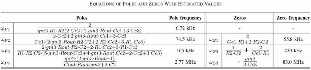
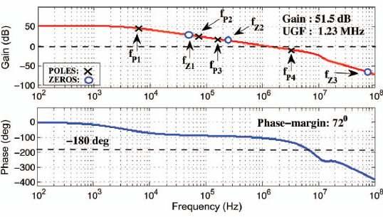
4 This 3 stage Class AB headphone driver incorporates all the desired features of an integrated audio amplifier. Apart from the output stage the proposed architecture is fully differential due to which there is low distortion even in low bias currents. Three Miller compensation networks are used so as to ensure stability. In addition to it the proposed architecture employs negetive biasing of the substrate which further reduces the total harmonic distortion.
5
6 The first two stages are fully differential amplifiers whereas the last stage is a push pull common source amplifier. First Stage: Its implemented with fully differential folded cascode amplifier using transistors M1-M12. M13-M20 along with the resistors form the CMFB. The gain of the first stage is given as A v1 = gm1.r1 ; where gm1 is the transconductance of M(3&4). Second Stage: The second stage is implemented with a pair of fully differential amplifier. This architecture is used as to have symmetric gain and pole frequencies at the output.
7 The output of the pmos differential amplifier is replicated to the output stage of the nmos common source amplifier M N. The quiescent current through M N and M P is computed as The design of the nmos differential amplifier is similar but the only difference is that the value of the resistors in the CMFB is changed to half of the value of that of pmos differential amplifier. This is done as in the output stage the input capacitanc e of the pmos is twice as that of nmos. Hence the value of resistors in CMFB are halved sized so as to obtain poles for both the transistors design on the same frequency.
8 Output Stage The output stage consists of pmos and nmos common source amplifier. As the amount of current required to drive the load is high and also the mobility of the electrons are twice as that of holes the width of the pmos transistor is made twice as that of nmos to attain equal strength for push pull action. The gate of transistor M P is biased at V DD V SG,58 by the nmos differential amplifier in the second stage. Similarly the gate of transistor M N is biased at V SS +V GS,39. Since the threshold voltages are not the same in 0.5µm process we used negative substrate bias of 1.5V so that swing at the gates of M P and M N are same, and also it reduces harmonic distortion by 8dB.
9 Small Signal Model and Compensation Network
10 Miller Compensation is used in this design to achieve the required stability. From the small signal model we can see that the resistor R C1 and capacitor C C1 are used between the output of the final stage and inverting output terminal of the first stage. This network determines the dominant pole of the amplifier. In order to achieve the same pole frequency at the output Miller capacitor C C3 is used at the output of the noninverting terminal of second stage pmos differential amplifier and a Miller capacitor of 2.C C3 is used at the output of non inverting terminal of the second stage nmos differential amplifier.
11 Poles And Zeroes The low frequency gain of this audio amplifier is given by A V = g m1 R1. g m2 R2. g m3 R out The proposed amplifier has 4 poles and two zeroes. From the analysis it is shown that two poles have been cancelled out by the two zeroes hence the system is a two pole system. The low frequency gain of the system is 51.5dB and the phase margin is 72 and the unity gain frequency of the amplifier is 1.23MHz from the analysis shown below.
12
13 Experimental Results
14 The measured response of the audio amplifier to a 200mV PP 50 khz square wave is shown for various capacitive loads in the above fig. No ringing was observed for capacitive loads from 10pF to 5nF and I L swinging from -25 to 25 ma. The slew rate is approximately 1.2 V/µs The quiescent current is measured 475µA for ± 1.5 V supply voltage. The above fig shows the output distortion for 1kHz sinusoidal input signal. As shown the harmonics are internally cancelled by fully differential first and second stage. The higher value of second harmonic distortion is due single ended output stage.
15 Power Supply Rejection Ratio The PSRR for V DD and V SS were also measured as shown in fig. Over entire audio freq range the PSRR from Vdd exceeds 63dB and for Vss it exceeds 66dB. As mentioned a high PSRR is a desirable feature in integrated amplifiers.
16 Conclusion: A process calledfigure of merit(fom) is used to signify the overall power efficiency of the audio amplifier and is given by FOM = Pp/Pq Where Pp is the peak power delivered to the load and Pq is the quiescent power of the amplifier. For the proposed amplifier design the vlue of FOM is higher than some of the other design published. Hence this design exhibits the highest power efficiency of any comparable design.
MANY PORTABLE devices available in the market, such
 IEEE TRANSACTIONS ON CIRCUITS AND SYSTEMS II: EXPRESS BRIEFS, VOL. 59, NO. 3, MARCH 2012 133 A 16-Ω Audio Amplifier With 93.8-mW Peak Load Power and 1.43-mW Quiescent Power Consumption Chaitanya Mohan,
ECEN 474/704 Lab 5: Frequency Response of Inverting Amplifiers
 ECEN 474/704 Lab 5: Frequency Response of Inverting Amplifiers Objective Design, simulate and layout various inverting amplifiers. Introduction Inverting amplifiers are fundamental building blocks of electronic
Advanced Operational Amplifiers
 IsLab Analog Integrated Circuit Design OPA2-47 Advanced Operational Amplifiers כ Kyungpook National University IsLab Analog Integrated Circuit Design OPA2-1 Advanced Current Mirrors and Opamps Two-stage
A High-Driving Class-AB Buffer Amplifier with a New Pseudo Source Follower
 A High-Driving Class-AB Buffer Amplifier with a New Pseudo Source Follower Chih-Wen Lu, Yen-Chih Shen and Meng-Lieh Sheu Abstract A high-driving class-ab buffer amplifier, which consists of a high-gain
TWO AND ONE STAGES OTA
 TWO AND ONE STAGES OTA F. Maloberti Department of Electronics Integrated Microsystem Group University of Pavia, 7100 Pavia, Italy franco@ele.unipv.it tel. +39-38-50505; fax. +39-038-505677 474 EE Department
A PSEUDO-CLASS-AB TELESCOPIC-CASCODE OPERATIONAL AMPLIFIER
 A PSEUDO-CLASS-AB TELESCOPIC-CASCODE OPERATIONAL AMPLIFIER M. Taherzadeh-Sani, R. Lotfi, and O. Shoaei ABSTRACT A novel class-ab architecture for single-stage operational amplifiers is presented. The structure
Radivoje Đurić, 2015, Analogna Integrisana Kola 1
 Low power OTA 1 Two-Stage, Miller Op Amp Operating in Weak Inversion Low frequency response: gm1 gm6 Av 0 g g g g A v 0 ds2 ds4 ds6 ds7 I D m, ds D nvt g g I n GB and SR: GB 1 1 n 1 2 4 6 6 7 g 2 2 m1
ECEN 474/704 Lab 6: Differential Pairs
 ECEN 474/704 Lab 6: Differential Pairs Objective Design, simulate and layout various differential pairs used in different types of differential amplifiers such as operational transconductance amplifiers
Chapter 12 Opertational Amplifier Circuits
 1 Chapter 12 Opertational Amplifier Circuits Learning Objectives 1) The design and analysis of the two basic CMOS op-amp architectures: the two-stage circuit and the single-stage, folded cascode circuit.
Design and Simulation of Low Voltage Operational Amplifier
 Design and Simulation of Low Voltage Operational Amplifier Zach Nelson Department of Electrical Engineering, University of Nevada, Las Vegas 4505 S Maryland Pkwy, Las Vegas, NV 89154 United States of America
A 24 V Chopper Offset-Stabilized Operational Amplifier with Symmetrical RC Notch Filters having sub-10 µv offset and over-120db CMRR
 ROMANIAN JOURNAL OF INFORMATION SCIENCE AND TECHNOLOGY Volume 20, Number 4, 2017, 301 312 A 24 V Chopper Offset-Stabilized Operational Amplifier with Symmetrical RC Notch Filters having sub-10 µv offset
Radivoje Đurić, 2015, Analogna Integrisana Kola 1
 OTA-output buffer 1 According to the types of loads, the driving capability of the output stages differs. For switched capacitor circuits which have high impedance capacitive loads, class A output stage
PART. Maxim Integrated Products 1
 - + 9-; Rev ; / Low-Cost, High-Slew-Rate, Rail-to-Rail I/O Op Amps in SC7 General Description The MAX9/MAX9/MAX9 single/dual/quad, low-cost CMOS op amps feature Rail-to-Rail input and output capability
Design of Miller Compensated Two-Stage Operational Amplifier for Data Converter Applications
 Design of Miller Compensated Two-Stage Operational Amplifier for Data Converter Applications Prema Kumar. G Shravan Kudikala Casest, School Of Physics Casest, School Of Physics University Of Hyderabad
Design of High-Speed Op-Amps for Signal Processing
 Design of High-Speed Op-Amps for Signal Processing R. Jacob (Jake) Baker, PhD, PE Professor and Chair Boise State University 1910 University Dr. Boise, ID 83725-2075 jbaker@ieee.org Abstract - As CMOS
Design Analysis and Performance Comparison of Low Power High Gain 2nd Stage Differential Amplifier Along with 1st Stage
 Design Analysis and Performance Comparison of Low Power High Gain 2nd Stage Differential Amplifier Along with 1st Stage Sadeque Reza Khan Department of Electronic and Communication Engineering, National
Lecture 300 Low Voltage Op Amps (3/28/10) Page 300-1
 Page 300-1") Lecture 300 Low Voltage Op Amps (3/28/10) Page 300-1 LECTURE 300 LOW VOLTAGE OP AMPS LECTURE ORGANIZATION Outline Introduction Low voltage input stages Low voltage gain stages Low voltage bias circuits
Lecture 300 Low Voltage Op Amps (3/28/10) Page 300-1 LECTURE 300 LOW VOLTAGE OP AMPS LECTURE ORGANIZATION Outline Introduction Low voltage input stages Low voltage gain stages Low voltage bias circuits
Analysis and Design of Analog Integrated Circuits Lecture 20. Advanced Opamp Topologies (Part II)
") Analysis and Design of Analog Integrated Circuits Lecture 20 Advanced Opamp Topologies (Part II) Michael H. Perrott April 15, 2012 Copyright 2012 by Michael H. Perrott All rights reserved. Outline of Lecture
Analysis and Design of Analog Integrated Circuits Lecture 20 Advanced Opamp Topologies (Part II) Michael H. Perrott April 15, 2012 Copyright 2012 by Michael H. Perrott All rights reserved. Outline of Lecture
A New Design Technique of CMOS Current Feed Back Operational Amplifier (CFOA)
") Circuits and Systems, 2013, 4, 11-15 http://dx.doi.org/10.4236/cs.2013.41003 Published Online January 2013 (http://www.scirp.org/journal/cs) A New Design Technique of CMOS Current Feed Back Operational
Circuits and Systems, 2013, 4, 11-15 http://dx.doi.org/10.4236/cs.2013.41003 Published Online January 2013 (http://www.scirp.org/journal/cs) A New Design Technique of CMOS Current Feed Back Operational
Rail-To-Rail Output Op-Amp Design with Negative Miller Capacitance Compensation
 Rail-To-Rail Op-Amp Design with Negative Miller Capacitance Compensation Muhaned Zaidi, Ian Grout, Abu Khari bin A ain Abstract In this paper, a two-stage op-amp design is considered using both Miller
Analog CMOS Interface Circuits for UMSI Chip of Environmental Monitoring Microsystem
 Analog CMOS Interface Circuits for UMSI Chip of Environmental Monitoring Microsystem A report Submitted to Canopus Systems Inc. Zuhail Sainudeen and Navid Yazdi Arizona State University July 2001 1. Overview
Design of a low voltage,low drop-out (LDO) voltage cmos regulator
 voltage cmos regulator") Design of a low,low drop-out (LDO) cmos regulator Chaithra T S Ashwini Abstract- In this paper a low, low drop-out (LDO) regulator design procedure is proposed and implemented using 0.25 micron CMOS process.
Design of a low,low drop-out (LDO) cmos regulator Chaithra T S Ashwini Abstract- In this paper a low, low drop-out (LDO) regulator design procedure is proposed and implemented using 0.25 micron CMOS process.
Class-AB Low-Voltage CMOS Unity-Gain Buffers
 Class-AB Low-Voltage CMOS Unity-Gain Buffers Mariano Jimenez, Antonio Torralba, Ramón G. Carvajal and J. Ramírez-Angulo Abstract Class-AB circuits, which are able to deal with currents several orders of
ISSN:
 468 Modeling and Design of a CMOS Low Drop-out (LDO) Voltage Regulator PRIYADARSHINI JAINAPUR 1, CHIRAG SHARMA 2 1 Department of E&CE, Nitte Meenakshi Institute of Technology, Yelahanka, Bangalore-560064,
Low Cost, General Purpose High Speed JFET Amplifier AD825
 a FEATURES High Speed 41 MHz, 3 db Bandwidth 125 V/ s Slew Rate 8 ns Settling Time Input Bias Current of 2 pa and Noise Current of 1 fa/ Hz Input Voltage Noise of 12 nv/ Hz Fully Specified Power Supplies:
Low Power Op-Amp Based on Weak Inversion with Miller-Cascoded Frequency Compensation
 Low Power Op-Amp Based on Weak Inversion with Miller-Cascoded Frequency Compensation Maryam Borhani, Farhad Razaghian Abstract A design for a rail-to-rail input and output operational amplifier is introduced.
Experiment 1: Amplifier Characterization Spring 2019
 Experiment 1: Amplifier Characterization Spring 2019 Objective: The objective of this experiment is to develop methods for characterizing key properties of operational amplifiers Note: We will be using
Analog Integrated Circuits. Lecture 7: OpampDesign
 Analog Integrated Circuits Lecture 7: OpampDesign ELC 601 Fall 2013 Dr. Ahmed Nader Dr. Mohamed M. Aboudina anader@ieee.org maboudina@gmail.com Department of Electronics and Communications Engineering
Amplifiers Frequency Response Examples
 ECE 5/45 Analog IC Design We will use the following MOSFET parameters for hand-calculations and the µm CMOS models for corresponding simulations. Table : Long-channel MOSFET parameters. Parameter NMOS
Topology Selection: Input
 Project #2: Design of an Operational Amplifier By: Adrian Ildefonso Nedeljko Karaulac I have neither given nor received any unauthorized assistance on this project. Process: Baker s 50nm CAD Tool: Cadence
Solid State Devices & Circuits. 18. Advanced Techniques
 ECE 442 Solid State Devices & Circuits 18. Advanced Techniques Jose E. Schutt-Aine Electrical l&c Computer Engineering i University of Illinois jschutt@emlab.uiuc.edu 1 Darlington Configuration - Popular
Low Quiescent Power CMOS Op-Amp in 0.5µm Technology
 Kevin Fronczak - Low Power CMOS Op-Amp - Rochester Institute of Technology EE610 1 Low Quiescent Power CMOS Op-Amp in 0.5µm Technology Kevin C. Fronczak Abstract This paper analyzes a low quiescent power
NOWADAYS, multistage amplifiers are growing in demand
 1690 IEEE TRANSACTIONS ON CIRCUITS AND SYSTEMS I: REGULAR PAPERS, VOL. 51, NO. 9, SEPTEMBER 2004 Advances in Active-Feedback Frequency Compensation With Power Optimization and Transient Improvement Hoi
A CMOS Low-Voltage, High-Gain Op-Amp
 A CMOS Low-Voltage, High-Gain Op-Amp G N Lu and G Sou LEAM, Université Pierre et Marie Curie Case 203, 4 place Jussieu, 75252 Paris Cedex 05, France Telephone: (33 1) 44 27 75 11 Fax: (33 1) 44 27 48 37
G m /I D based Three stage Operational Amplifier Design
 G m /I D based Three stage Operational Amplifier Design Rishabh Shukla SVNIT, Surat shuklarishabh31081988@gmail.com Abstract A nested Gm-C compensated three stage Operational Amplifier is reviewed using
d. Can you find intrinsic gain more easily by examining the equation for current? Explain.
 EECS140 Final Spring 2017 Name SID 1. [8] In a vacuum tube, the plate (or anode) current is a function of the plate voltage (output) and the grid voltage (input). I P = k(v P + µv G ) 3/2 where µ is a
Microelectronic Circuits II. Ch 10 : Operational-Amplifier Circuits
 Microelectronic Circuits II Ch 0 : Operational-Amplifier Circuits 0. The Two-stage CMOS Op Amp 0.2 The Folded-Cascode CMOS Op Amp CNU EE 0.- Operational-Amplifier Introduction - Analog ICs : operational
SALLEN-KEY FILTERS USING OPERATIONAL TRANSCONDUCTANCE AMPLIFIER
 International Journal of Electronics and Communication Engineering and Technology (IJECET) Volume 8, Issue 3, May-June 2017, pp. 52 58, Article ID: IJECET_08_03_006 Available online at http://www.iaeme.com/ijecet/issues.asp?jtypeijecet&vtype8&itype3
Index. Small-Signal Models, 14 saturation current, 3, 5 Transistor Cutoff Frequency, 18 transconductance, 16, 22 transit time, 10
 Index A absolute value, 308 additional pole, 271 analog multiplier, 190 B BiCMOS,107 Bode plot, 266 base-emitter voltage, 16, 50 base-emitter voltages, 296 bias current, 111, 124, 133, 137, 166, 185 bipolar
Lecture 200 Cascode Op Amps - II (2/18/02) Page 200-1
 Page 200-1") Lecture 200 Cascode Op Amps II (2/18/02) Page 2001 LECTURE 200 CASCODE OP AMPS II (READING: GHLM 443453, AH 293309) Objective The objective of this presentation is: 1.) Develop cascode op amp architectures
Lecture 200 Cascode Op Amps II (2/18/02) Page 2001 LECTURE 200 CASCODE OP AMPS II (READING: GHLM 443453, AH 293309) Objective The objective of this presentation is: 1.) Develop cascode op amp architectures
Atypical op amp consists of a differential input stage,
 IEEE JOURNAL OF SOLID-STATE CIRCUITS, VOL. 33, NO. 6, JUNE 1998 915 Low-Voltage Class Buffers with Quiescent Current Control Fan You, S. H. K. Embabi, and Edgar Sánchez-Sinencio Abstract This paper presents
EECE488: Analog CMOS Integrated Circuit Design Set 7 Opamp Design
 EECE488: Analog CMOS Integrated Circuit Design Set 7 Opamp Design References: Analog Integrated Circuit Design by D. Johns and K. Martin and Design of Analog CMOS Integrated Circuits by B. Razavi All figures
Gechstudentszone.wordpress.com
 UNIT 4: Small Signal Analysis of Amplifiers 4.1 Basic FET Amplifiers In the last chapter, we described the operation of the FET, in particular the MOSFET, and analyzed and designed the dc response of circuits
Operational Amplifiers
 CHAPTER 9 Operational Amplifiers Analog IC Analysis and Design 9- Chih-Cheng Hsieh Outline. General Consideration. One-Stage Op Amps / Two-Stage Op Amps 3. Gain Boosting 4. Common-Mode Feedback 5. Input
Revision History. Contents
 Revision History Ver. # Rev. Date Rev. By Comment 0.0 9/15/2012 Initial draft 1.0 9/16/2012 Remove class A part 2.0 9/17/2012 Comments and problem 2 added 3.0 10/3/2012 cmdmprobe re-simulation, add supplement
Operational Amplifiers
 Questions Easy Operational Amplifiers 1. Which of the following statements are true? a. An op-amp has two inputs and three outputs b. An op-amp has one input and two outputs c. An op-amp has two inputs
ECE 415/515 ANALOG INTEGRATED CIRCUIT DESIGN
 ECE 415/515 ANALOG INTEGRATED CIRCUIT DESIGN OPAMP DESIGN AND SIMULATION Vishal Saxena OPAMP DESIGN PROJECT R 2 v out v in /2 R 1 C L v in v out V CM R L V CM C L V CM -v in /2 R 1 C L (a) (b) R 2 ECE415/EO
Lecture 240 Cascode Op Amps (3/28/10) Page 240-1
 Page 240-1") Lecture 240 Cascode Op Amps (3/28/10) Page 2401 LECTURE 240 CASCODE OP AMPS LECTURE ORGANIZATION Outline Lecture Organization Single Stage Cascode Op Amps Two Stage Cascode Op Amps Summary CMOS Analog
Lecture 240 Cascode Op Amps (3/28/10) Page 2401 LECTURE 240 CASCODE OP AMPS LECTURE ORGANIZATION Outline Lecture Organization Single Stage Cascode Op Amps Two Stage Cascode Op Amps Summary CMOS Analog
IOWA STATE UNIVERSITY. EE501 Project. Fully Differential Multi-Stage Op-Amp Design. Ryan Boesch 11/12/2008
 IOWA STATE UNIVERSITY EE501 Project Fully Differential Multi-Stage Op-Amp Design Ryan Boesch 11/12/2008 This report documents the design, simulation, layout, and post-layout simulation of a fully differential
ECEN474: (Analog) VLSI Circuit Design Fall 2011
 VLSI Circuit Design Fall 2011") ECEN474: (Analog) VLSI Circuit Design Fall 20 Lecture 22: Output Stages Sebastian Hoyos Analog & Mixed-Signal Center Texas A&M University Agenda Output Stages Source Follower (Class A) Push-Pull (Class
ECEN474: (Analog) VLSI Circuit Design Fall 20 Lecture 22: Output Stages Sebastian Hoyos Analog & Mixed-Signal Center Texas A&M University Agenda Output Stages Source Follower (Class A) Push-Pull (Class
An Analog Phase-Locked Loop
 1 An Analog Phase-Locked Loop Greg Flewelling ABSTRACT This report discusses the design, simulation, and layout of an Analog Phase-Locked Loop (APLL). The circuit consists of five major parts: A differential
A new class AB folded-cascode operational amplifier
 A new class AB folded-cascode operational amplifier Mohammad Yavari a) Integrated Circuits Design Laboratory, Department of Electrical Engineering, Amirkabir University of Technology, Tehran, Iran a) myavari@aut.ac.ir
CLASS AB amplifiers have a wide range of applications in
 IEEE TRANSATIONS ON IRUITS AND SYSTEMS II: EXPRESS BRIEFS onverting a Three- Pseudo-lass AB Amplifier to a True lass AB Amplifier Punith R. Surkanti, Student Member, IEEE and Paul M. Furth, Senior Member,
Microelectronics Exercises of Topic 5 ICT Systems Engineering EPSEM - UPC
 Microelectronics Exercises of Topic 5 ICT Systems Engineering EPSEM - UPC F. Xavier Moncunill Autumn 2018 5 Analog integrated circuits Exercise 5.1 This problem aims to follow the steps in the design of
Design of a Sample and Hold Circuit using Rail to Rail Low Voltage Compact Operational Amplifier and bootstrap Switching
 RESEARCH ARTICLE OPEN ACCESS Design of a Sample and Hold Circuit using Rail to Rail Low Voltage Compact Operational Amplifier and bootstrap Switching Annu Saini, Prity Yadav (M.Tech. Student, Department
Rail to Rail Input Amplifier with constant G M and High Unity Gain Frequency. Arun Ramamurthy, Amit M. Jain, Anuj Gupta
 1 Rail to Rail Input Amplifier with constant G M and High Frequency Arun Ramamurthy, Amit M. Jain, Anuj Gupta Abstract A rail to rail input, 2.5V CMOS input amplifier is designed that amplifies uniformly
DESIGN HIGH SPEED, LOW NOISE, LOW POWER TWO STAGE CMOS OPERATIONAL AMPLIFIER. Himanshu Shekhar* 1, Amit Rajput 1
 ISSN 2277-2685 IJESR/June 2014/ Vol-4/Issue-6/319-323 Himanshu Shekhar et al./ International Journal of Engineering & Science Research DESIGN HIGH SPEED, LOW NOISE, LOW POWER TWO STAGE CMOS OPERATIONAL
Performance Analysis of Low Power, High Gain Operational Amplifier Using CMOS VLSI Design
 RESEARCH ARTICLE OPEN ACCESS Performance Analysis of Low Power, High Gain Operational Amplifier Using CMOS VLSI Design Ankush S. Patharkar*, Dr. Shirish M. Deshmukh** *(Department of Electronics and Telecommunication,
A 100MHz CMOS wideband IF amplifier
 A 100MHz CMOS wideband IF amplifier Sjöland, Henrik; Mattisson, Sven Published in: IEEE Journal of Solid-State Circuits DOI: 10.1109/4.663569 1998 Link to publication Citation for published version (APA):
Advanced OPAMP Design
 Advanced OPAMP Design Two Stage OPAMP with Cascoding To increase the gain, the idea of cascoding can be combined with the idea of cascading. A two stage amplifier with one stage being cascode is possible.
Basic OpAmp Design and Compensation. Chapter 6
 Basic OpAmp Design and Compensation Chapter 6 6.1 OpAmp applications Typical applications of OpAmps in analog integrated circuits: (a) Amplification and filtering (b) Biasing and regulation (c) Switched-capacitor
A Unity Gain Fully-Differential 10bit and 40MSps Sample-And-Hold Amplifier in 0.18μm CMOS
 A Unity Gain Fully-Differential 0bit and 40MSps Sample-And-Hold Amplifier in 0.8μm CMOS Sanaz Haddadian, and Rahele Hedayati Abstract A 0bit, 40 MSps, sample and hold, implemented in 0.8-μm CMOS technology
HT9274 Quad Micropower Op Amp
 Quad Micropower Op Amp Features Quad micro power op amp Wide range of supply voltage: 1.6V~5.5V High input impedance Single supply operation Low current consumption: < 5A per amp Rail to rail output Provides
DESIGN OF TWO-STAGE CLASS AB CASCODE OP-AMP WITH IMPROVED GAIN
 DESIGN OF TWO-STAGE CLASS AB CASCODE OP-AMP WITH IMPROVED GAIN 1 B.Hinduja, 2 Dr.G.V. Maha Lakshmi 1 PG Scholar, 2 Professor Department of Electronics and Communication Engineering Sreenidhi Institute
Chapter 5. Operational Amplifiers and Source Followers. 5.1 Operational Amplifier
 Chapter 5 Operational Amplifiers and Source Followers 5.1 Operational Amplifier In single ended operation the output is measured with respect to a fixed potential, usually ground, whereas in double-ended
James Lunsford HW2 2/7/2017 ECEN 607
 James Lunsford HW2 2/7/2017 ECEN 607 Problem 1 Part A Figure 1: Negative Impedance Converter To find the input impedance of the above NIC, we use the following equations: V + Z N V O Z N = I in, V O kr
An Ultra Low-Voltage and Low-Power OTA Using Bulk-Input Technique and Its Application in Active-RC Filters
 Circuits and Systems, 2011, 2, 183-189 doi:10.4236/cs.2011.23026 Published Online July 2011 (http://www.scirp.org/journal/cs) An Ultra Low-Voltage and Low-Power OTA Using Bulk-Input Technique and Its Application
Inter-Ing INTERDISCIPLINARITY IN ENGINEERING SCIENTIFIC INTERNATIONAL CONFERENCE, TG. MUREŞ ROMÂNIA, November 2007.
 Inter-Ing 2007 INTERDISCIPLINARITY IN ENGINEERING SCIENTIFIC INTERNATIONAL CONFERENCE, TG. MUREŞ ROMÂNIA, 15-16 November 2007. A FULLY BALANCED, CCII-BASED TRANSCONDUCTANCE AMPLIFIER AND ITS APPLICATION
You will be asked to make the following statement and provide your signature on the top of your solutions.
 1 EE 435 Name Exam 1 Spring 216 Instructions: The points allocated to each problem are as indicated. Note that the first and last problem are weighted more heavily than the rest of the problems. On those
CMOS Operational Amplifier
 The George Washington University Department of Electrical and Computer Engineering Course: ECE218 Instructor: Mona E. Zaghloul Students: Shunping Wang Yiping (Neil) Tsai Data: 05/14/07 Introduction In
A low voltage rail-to-rail operational amplifier with constant operation and improved process robustness
 Graduate Theses and Dissertations Graduate College 2009 A low voltage rail-to-rail operational amplifier with constant operation and improved process robustness Rien Lerone Beal Iowa State University Follow
Op-Amp Design Project EE 5333 Analog Integrated Circuits Prof. Ramesh Harjani Department of ECE University of Minnesota, Twin Cities Report prepared
 Op-Amp Design Project EE 5333 Analog Integrated Circuits Prof. Ramesh Harjani Department of ECE University of Minnesota, Twin Cities Report prepared by: Nirav Desai (4280229) 1 Contents: 1. Design Specifications
High Voltage and Temperature Auto Zero Op-Amp Cell Features Applications Process Technology Introduction Parameter Unit Rating
 Analogue Integration AISC11 High Voltage and Temperature Auto Zero Op-Amp Cell Rev.1 12-1-5 Features High Voltage Operation: 4.5-3 V Precision, Auto-Zeroed Input Vos High Temperature Operation Low Quiescent
Basic distortion definitions
 Conclusions The push-pull second-generation current-conveyor realised with a complementary bipolar integration technology is probably the most appropriate choice as a building block for low-distortion
Comparative Analysis of Compensation Techniques for improving PSRR of an OPAMP
 Comparative Analysis of Compensation Techniques for improving PSRR of an OPAMP 1 Pathak Jay, 2 Sanjay Kumar M.Tech VLSI and Embedded System Design, Department of School of Electronics, KIIT University,
Sensors & Transducers Published by IFSA Publishing, S. L.,
 Sensors & Transducers Published by IFSA Publishing, S. L., 208 http://www.sensorsportal.com Fully Differential Operation Amplifier Using Self Cascode MOSFET Structure for High Slew Rate Applications Kalpraj
IJSRD - International Journal for Scientific Research & Development Vol. 4, Issue 02, 2016 ISSN (online):
:") IJSRD - International Journal for Scientific Research & Development Vol. 4, Issue 02, 2016 ISSN (online): 2321-0613 Design & Analysis of CMOS Telescopic Operational Transconductance Amplifier (OTA) with
IJSRD - International Journal for Scientific Research & Development Vol. 4, Issue 02, 2016 ISSN (online): 2321-0613 Design & Analysis of CMOS Telescopic Operational Transconductance Amplifier (OTA) with
ECEN 474/704 Lab 7: Operational Transconductance Amplifiers
 ECEN 474/704 Lab 7: Operational Transconductance Amplifiers Objective Design, simulate and layout an operational transconductance amplifier. Introduction The operational transconductance amplifier (OTA)
A Compact 2.4V Power-efficient Rail-to-rail Operational Amplifier. Strong inversion operation stops a proposed compact 3V power-efficient
 A Compact 2.4V Power-efficient Rail-to-rail Operational Amplifier Abstract Strong inversion operation stops a proposed compact 3V power-efficient rail-to-rail Op-Amp from a lower total supply voltage.
DUAL ULTRA MICROPOWER RAIL-TO-RAIL CMOS OPERATIONAL AMPLIFIER
 ADVANCED LINEAR DEVICES, INC. ALD276A/ALD276B ALD276 DUAL ULTRA MICROPOWER RAILTORAIL CMOS OPERATIONAL AMPLIFIER GENERAL DESCRIPTION The ALD276 is a dual monolithic CMOS micropower high slewrate operational
ELM824xA 3.0μA Very low power CMOS dual operational amplifier
 ELM824xA 3.μA Very low power CMOS dual operational amplifier General description ELM824xA is a very low current consumption-typ.3.μa CMOS dual OP-AMP provided with a wide common mode input voltage range.
Design and Simulation of Low Dropout Regulator
 Design and Simulation of Low Dropout Regulator Chaitra S Kumar 1, K Sujatha 2 1 MTech Student, Department of Electronics, BMSCE, Bangalore, India 2 Assistant Professor, Department of Electronics, BMSCE,
CMOS Instrumentation Amplifier with Offset Cancellation Circuitry for Biomedical Application
 CMOS Instrumentation Amplifier with Offset Cancellation Circuitry for Biomedical Application Author Mohd-Yasin, Faisal, Yap, M., I Reaz, M. Published 2006 Conference Title 5th WSEAS Int. Conference on
Dual operational amplifier
 DESCRIPTION The 77 is a pair of high-performance monolithic operational amplifiers constructed on a single silicon chip. High common-mode voltage range and absence of latch-up make the 77 ideal for use
Research Article A Robust Low-Voltage On-Chip LDO Voltage Regulator in 180 nm
 VLSI Design Volume 2008, Article ID 259281, 7 pages doi:10.1155/2008/259281 Research Article A Robust Low-Voltage On-Chip LDO Voltage Regulator in 180 nm Sreehari Rao Patri and K. S. R. Krishna Prasad
University of Michigan, EECS413 Final project. A High Speed Operational Amplifier. 1. A High Speed Operational Amplifier
 University of Michigan, EECS413 Final project. A High Speed Operational Amplifier. 1 A High Speed Operational Amplifier A. Halim El-Saadi, Mohammed El-Tanani, University of Michigan Abstract This paper
A Compact Folded-cascode Operational Amplifier with Class-AB Output Stage
 A Compact Folded-cascode Operational Amplifier with Class-AB Output Stage EEE 523 Advanced Analog Integrated Circuits Project Report Fuding Ge You are an engineer who is assigned the project to design
POWER-MANAGEMENT circuits are becoming more important
 174 IEEE TRANSACTIONS ON CIRCUITS AND SYSTEMS II: EXPRESS BRIEFS, VOL. 58, NO. 3, MARCH 2011 Dynamic Bias-Current Boosting Technique for Ultralow-Power Low-Dropout Regulator in Biomedical Applications
[Kumar, 2(9): September, 2013] ISSN: Impact Factor: 1.852
![[Kumar, 2(9): September, 2013] ISSN: Impact Factor: 1.852](/thumbs/86/94008668.jpg "[Kumar, 2(9): September, 2013] ISSN: Impact Factor: 1.852") IJESRT INTERNATIONAL JOURNAL OF ENGINEERING SCIENCES & RESEARCH TECHNOLOGY Design and Performance analysis of Low power CMOS Op-Amp Anand Kumar Singh *1, Anuradha 2, Dr. Vijay Nath 3 *1,2 Department of
IJESRT INTERNATIONAL JOURNAL OF ENGINEERING SCIENCES & RESEARCH TECHNOLOGY Design and Performance analysis of Low power CMOS Op-Amp Anand Kumar Singh *1, Anuradha 2, Dr. Vijay Nath 3 *1,2 Department of
Design of Rail-to-Rail Op-Amp in 90nm Technology
 IJSTE - International Journal of Science Technology & Engineering Volume 1 Issue 2 August 2014 ISSN(online) : 2349-784X Design of Rail-to-Rail Op-Amp in 90nm Technology P R Pournima M.Tech Electronics
Design of an Amplifier for Sensor Interfaces
 Design of an Amplifier for Sensor Interfaces Anurag Mangla Electrical and Electronics Engineering anurag.mangla@epfl.ch Supervised by Dr. Marc Pastre Prof. Maher Kayal Outline Introduction Need for high
Basic Circuits. Current Mirror, Gain stage, Source Follower, Cascode, Differential Pair,
 Basic Circuits Current Mirror, Gain stage, Source Follower, Cascode, Differential Pair, CCS - Basic Circuits P. Fischer, ZITI, Uni Heidelberg, Seite 1 Reminder: Effect of Transistor Sizes Very crude classification:
DESIGN OF 2.4 GHZ LOW POWER CMOS TRANSMITTER FRONT END
 Volume 117 No. 16 2017, 685-694 ISSN: 1311-8080 (printed version); ISSN: 1314-3395 (on-line version) url: http://www.ijpam.eu ijpam.eu DESIGN OF 2.4 GHZ LOW POWER CMOS TRANSMITTER FRONT END 1 S.Manjula,
Operational Amplifier with Two-Stage Gain-Boost
 Proceedings of the 6th WSEAS International Conference on Simulation, Modelling and Optimization, Lisbon, Portugal, September 22-24, 2006 482 Operational Amplifier with Two-Stage Gain-Boost FRANZ SCHLÖGL
BJT Circuits (MCQs of Moderate Complexity)
") BJT Circuits (MCQs of Moderate Complexity) 1. The current ib through base of a silicon npn transistor is 1+0.1 cos (1000πt) ma. At 300K, the rπ in the small signal model of the transistor is i b B C r
BJT Circuits (MCQs of Moderate Complexity) 1. The current ib through base of a silicon npn transistor is 1+0.1 cos (1000πt) ma. At 300K, the rπ in the small signal model of the transistor is i b B C r
CMOS Operational-Amplifier
 CMOS Operational-Amplifier 1 What will we learn in this course How to design a good OP Amp. Basic building blocks Biasing and Loading Swings and Bandwidth CH2(8) Operational Amplifier as A Black Box Copyright
Ultra Low Static Power OTA with Slew Rate Enhancement
 ECE 595B Analog IC Design Design Project Fall 2009 Project Proposal Ultra Low Static Power OTA with Slew Rate Enhancement Patrick Wesskamp PUID: 00230-83995 1) Introduction In this design project I plan
EE 501 Lab 10 Output Amplifier Due: December 10th, 2015
 EE 501 Lab 10 Output Amplifier Due: December 10th, 2015 Objective: Get familiar with output amplifier. Design an output amplifier driving small resistor load. Design an output amplifier driving large capacitive
CMOS Operational-Amplifier
 CMOS Operational-Amplifier 1 What will we learn in this course How to design a good OP Amp. Basic building blocks Biasing and Loading Swings and Bandwidth CH2(8) Operational Amplifier as A Black Box Copyright
Nonlinear Macromodeling of Amplifiers and Applications to Filter Design.
 ECEN 622(ESS) Nonlinear Macromodeling of Amplifiers and Applications to Filter Design. By Edgar Sanchez-Sinencio Thanks to Heng Zhang for part of the material OP AMP MACROMODELS Systems containing a significant