Revision History. Contents
|
|
|
- Roberta Ryan
- 5 years ago
- Views:
Transcription
1 Revision History Ver. # Rev. Date Rev. By Comment 0.0 9/15/2012 Initial draft 1.0 9/16/2012 Remove class A part 2.0 9/17/2012 Comments and problem 2 added /3/2012 cmdmprobe re-simulation, add supplement Contents 1 TWO-STAGE FULLY-DIFFERENTIAL OPAMP DESIGN SPEC. AND REQUIREMENT CIRCUIT DESIGN AND TEST BENCH Bias Circuit Two-Stage Fully Differential Circuit Simulation Test Bench SIMULATION RESULTS AND SUMMARY Open loop AC simulation Resistive Feedback AC simulation Fully Differential Opamp in feedback loop stability analysis Differential/Common Mode Transient Response PAPER DIGEST PAPER 1 [1] PAPER 2 [2] PAPER 3 [3] PAPER 4 [4] CMFB USING TRIODE DEVICES [5] SIMULATION SUPPLEMENT METHOD METHOD REFERENCES
2 Table of Figures Figure 1 Bias generation circuit schematic Figure 2 Schematic of 2-stage fully differential circuit with class AB output stage Figure 3 Two-stage common-mode picture Figure 4 Closed loop stability analysis test bench Figure 5 Closed loop stb analysis test bench using cmdmprobe method Figure 6 Closed loop stb analysis test bench using cmdmprobe method Figure 7 Differential open loop AC simulation test bench Figure 8 Differential closed loop AC simulation test bench Figure 9 Unity-gain inverter transient simulation test bench for differential mode step response Figure 10 Unity-gain inverter transient simulation test bench for common mode step response Figure 11 Differential open loop bode plot Figure 12 Close loop AC simulation bode plot and summary Figure 13 Close loop AC simulation magnitude plot when configured at unity-gain Figure 14 First stage CMFB stb analysis with cmdmprobe Figure 15 First stage CMFB stb analysis with iprobe Figure 16 Second stage CMFB stb analysis with cmdmprobe Figure 17 Second stage CMFB stb analysis with iprobe Figure 18 Two-stage class AB closed loop stb analysis with cmdmprobe Figure 19 Closed loop bode plot configured as unity gain inverter using cmdmprobe stb analysis Figure 20 Unity- gain inverting amplifier transient response with a 200mV differential step (rise/fall time=0.1ns, pulse with=100ns, in test bench set output VCVS gain=-1) Figure 21 Unity- gain inverting amplifier transient response with a 100mV common mode step (rise/fall time=0.1ns, pulse with=100ns, in the test bench veriloga adder is used for averaging) Figure 22 Operational amplifier used in the first integrator. (a) Main amplifier. (b) Common-mode feedback (CMFB) for the first stage. (c) Second-stage CMFB circuit Figure 23 Schematic of the operational amplifier used in the second and third integrators and the summing amplifier Figure 24 Operational amplifier used in the first integrator in paper Figure 25 Feedforward compensated opamp used in the paper 3. Feedforward path is shown in bold, and CMFB paths are shown in gray Figure 26 Feedforward compensated opamp used in the summing amplifier. Feedforward path is shown in bold, and CMFB paths are shown in gray Figure 27 Feedforward opamp schematic, including common-mode feedback Figure 28 CMFB using triode devices Figure 29 DM loop Method 1 and 2 the same Figure 30 2 nd stage CMFB Method Figure 31 1 st stage CMFB Method Figure 32 2 nd stage CMFB Method Figure 33 1 st stage CMFB Method List of tables Table 1 Summary and comparison of stb analysis for the three feedback loops at tt corner
3 1 Two-stage fully-differential Opamp design 1.1 Spec. and Requirement Process: IBM 130nm CMOS, 1.2V nominal power supply voltage. Specification: Closed loop gain and -3dB bandwidth are 2 and 20MHz, respectively. C L = 5pF. Rail-to-rail output swing. Open loop gain 70dB. V CM = V DD /2. Requirements: individual CMFB loops; No systematic offset in CMFB loops; Compensate all the three feedback loops for PM of 60º. Pass tt and ssf corners. Simulation list: 1. Differential open loop gain-magnitude and phase. Indicate the phase margin. 2. Differential closed loop gain-magnitude and phase. Indicate the -3 db bandwidth. 3. First stage common-mode loop gain-magnitude and phase. Indicate the phase margin. 4. Second stage common-mode loop gain-magnitude and phase. Indicate the phase margin. 5. Transient response of the unity-gain inverting amplifier with a 200 mv differential step (use 0.1 ns rise/fall times). 6. Transient response of the unity-gain inverting amplifier with a 100 mv common mode step (use 0.1 ns rise/fall times). 1.2 Circuit Design and Test Bench In order to go through the CFMB and compensation theory, Class A output is first designed. Then Class AB output stage is implemented. Here, only class AB topology result is shown. ADE XL is used to do corner simulation. Schematic simulation are performed at 1.2V power supply, 40ºC temperature, tt and ssf corners Bias Circuit Bias circuit generates voltages for vb1, vb2, vb3, vb4 used to bias the current source/sink used in the fully differential opamps. Assume we get a reference voltage of 600mV and a 10 µa@27ºc PTAT current from BGR. As a rule of thumb, set the temperate coefficient of the PTAT current to be 0.067µA/ºC in the simulation. A regulated current reference with external precision 60K Ohm resistor to generate a 10µA current into high swing current source to generate bias voltages for the opamp. 20/0.8 12/0.8 12/0.8 6/0.8 5/1.52 8/0.35 8/0.35 4/0.35 4/0.35 Id=10µ+(temp-27)* /0.8 25/0.5 ESD sensitive node 10/0.3 5/1.5 5/0.3 10/1 20/1 10/1.5 5/5 5/1.5 External res & parasitic cap Figure 1 Bias generation circuit schematic. 3
4 1.2.2 Two-Stage Fully Differential Circuit Opamp topology: Folded-cascode opamp topology is chosen as the first stage for 1.2V nominal power supply and to obtain high DC gain. Class AB output stage is used to extend the signal swing. Separate CMFB scheme is used for both stages to set each output to well defined common mode voltage level, here is 600mV. The quiescent output voltage at nodes vop1 and von1 sets the quiescent currents in the second stage [1]. Look at the common mode picture as shown in Fig 3, at high frequencies, the 2 nd -stage compensation capacitor 2C C can be considered as short, the common mode output impedance of the class AB consists of the parallel combination of the positive resistance of the diode connected (through 2C C ) transistor M8 and the negative resistance formed by the loop M4-M6-M7. In the presence of mismatches, it is possible for the common mode output impedance to have a negative real part and lead to instability. To prevent this and ensure stability and reliable operation of the CMFB loop, quiescent current in the upper PMOS, which contributes to the positive resistance, should be made larger than quiescent current in the lower NMOS [1]. My design missed this point! CMFB topology: Since the output swings of the first stage is modest in closed loop applications, the linearity of the common mode detector is not critical [1]. we can use Dual-Diff amp scheme to merge the CM detector and the error amplifier as a one. And it doesn t load the first stage that much. For class AB output stage, since the signal swings are large, linear operation of the CMFB mechanism is ensured by using resistive averaging to detect the output common mode. Parallel cap is added to form high frequency path to cancel the pole introduced by the parasitic cap of the error amplify input pair. The resistor should be large enough to ensure high output impedance. The feedback node is acting as a VCCS to control the gate of a PMOS by injecting current to tune output common mode level. Compensation: There are two internal common mode feedback loops and one external feedback loop, so that the circuit should be compensated to ensure stability. For the 2-stage opamp and 1 st - stage CMFB loop, miller compensation is simply used. The 2 nd -stage CMFB loop is also a 2-stage opamp as can be clearly seen in the CM picture illustrated in Fig 3. In order to make sure the loop is stable and avoid using miller cap loading the output, I just change the load of the error amplify to diode connected, make it one pole system but sacrifice the gain. Actually, it may be better to use miller compensation for higher gain and smaller systematic offset introduced by matching. But I have limited time to go back and re-simulate. Minimize systematic offset: The current density in the error amplify should be matched to the current density in the main stage opamp. The gates bias of current source of the second stage CMFB error amplify are tied as shown in Fig2. Since it s diode connected load, the W/L of the PMOS load is a little different with the W/L of the feedback controlled PMOS. 4
5 50µ 50µ 4I O I O vcmfb2 12/0.5 48/0.5 12/0.5 von 5/1.6 vbn_l 10/0.4 60/0.8 8/0.35 vop1 10/0.3 50/0.4 10/1.5 vcmfb1 vp 160/0.5 80/0.3 80/1.5 vcmfb1 vn von1 vbn_r 12/0.8 vcmfb2 2/0.5 vop 12/ K vcmfb1 vcmfb2 300K 4/0.5 2/0.5 4/0.5 4/0.5 20/0.3 vbn_l vbn_r 20/1.5 10/ f 5I O I O 10µ 80µ 10µ 5I O 20µ I O 2I O 1 st -stage CMFB 2 nd -stage CMFB 13K 680f bias 1.03K 2p vop1 von von1 vop vop1 vcmfb1 von1 Miller compensation for 2 nd -stage opamp Miller compensation for 1 st -stage CMFB Figure 2 Schematic of 2-stage fully differential circuit with class AB output stage. Loop 1 M4 M9 M8 Incorrect place to insert iprobe R Z /2 2C C M5 M6 M7 Loop 2 Figure 3 Two-stage common-mode picture Simulation Test Bench Open loop and closed loop frequency analysis are performed by AC simulation. Fig 4 is used to perform stability analysis for common mode loop and closed loop of the fully differential opamp. For CMFB loop, usually there have two places can break the loop, which are differential input sensing nodes or single-ended control node at the output of the error amplify. For differential nodes, we use cmdmprobe and set CMDM=1, for singleended node, we simply use iprobe. One thing worth to mention is that, if probe is placed between two high impedance nodes, results obtained by using cmdmprobe and iprobe are all the same (eg. Loop 1). While, for loop 2, the output of the error amplifier is not a high impedance node, so that it s not correct to use iprobe (indicated in Fig 4) for the second stage CMFB stability analysis. Differential mode and common mode transient responses are checked in the end. 5
6 vcmfb1 vcmfb1 vcmfb2 vcmfb2 vcmfb1 von vop1 vp vn von1 vop1 von1 vop vcmfb2 Low impedance node vop von vn vp vop von vop1 von von1 vop vop1 von1 vcmfb1 bias The 2-stage opamp schematic inside the symbol is shown right above Figure 4 Closed loop stability analysis test bench. Figure 5 Closed loop stb analysis test bench using cmdmprobe method 1. Figure 6 Closed loop stb analysis test bench using cmdmprobe method 2 6
7 Figure 7 Differential open loop AC simulation test bench. Figure 8 Differential closed loop AC simulation test bench. Figure 9 Unity-gain inverter transient simulation test bench for differential mode step response. 7
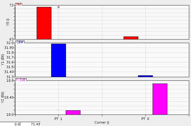
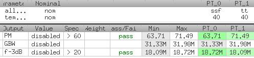
8 Figure 10 Unity-gain inverter transient simulation test bench for common mode step response. 1.3 Simulation Results and Summary Simulation results are obtained with the test benches described above. First, by using DC and AC simulation to check the DC node voltages and open loop opamp specifications. In resistive feedback AC simulation, as shown in Fig11, the calculator expression seems not match the bode plot. Then, closed loop stability analysis is followed to ensure the three feedback loops in the system are stable. Last, transient simulation is performed to see the differential and common mode responses. In conclusion, all simulation under 40ºC, 1.2V power supply, ssf and tt corner, the open loop DC gain is higher than 70dB. Table 1 summarized and compared the aforementioned three loops by using cmdmprobe and iprobe stb analysis. It shows that for CMFB loop 2, iprobe is not accurate due to low impedance node, its PM got from cmdmprobe seems too large and it should be improved later on. DC current consumption of the fully differential opamp at ssf and tt corner is 1.35mA and 1.86mA, respectively, all at 1.2V power supply and 40ºC Open loop AC simulation 8


9 Figure 11 Differential open loop bode plot Resistive Feedback AC simulation 9

10 Figure 12 Close loop AC simulation bode plot and summary. 10

.")
11 Figure 13 Close loop AC simulation magnitude plot when configured at unity-gain Fully Differential Opamp in feedback loop stability analysis When analysis common mode loop stability, CMDM should be set as 1 in the cmdmprobe property. For first stage CMFB loop, the results obtained by using cmdmprobe and iprobe match quite well (refer to Fig 14 and Fig 15). While, for the second stage CMFB loop, the results got by using different probes are different (see Fig.16 and Fig 17) due the low impedance node at output of the 2 nd stage error amplifier as shown in Fig 4. Figure 14 First stage CMFB stb analysis with cmdmprobe. 11


12 Figure 15 First stage CMFB stb analysis with iprobe. Figure 16 Second stage CMFB stb analysis with cmdmprobe. 12


13 Figure 17 Second stage CMFB stb analysis with iprobe. Figure 18 Two-stage class AB closed loop stb analysis with cmdmprobe. 13

14 Table 1 Summary and comparison of stb analysis for the three feedback loops at tt corner. Items DC Gain (db) PM (º) GBW (MHz) stb options CMDM=1 1 st stage CMFB NA NA NA CMDM= iprobe CMDM=1 2 nd stage CMFB NA NA NA CMDM= Misused iprobe Closed loop NA NA CMDM= (correct?) CMDM=-1 When it configured as unity-gain feedback, the phase margin drops! Figure 19 Closed loop bode plot configured as unity gain inverter using cmdmprobe stb analysis Differential/Common Mode Transient Response Transient simulations are performed to test differential mode and common mode responses when the opamp is configured in unity gain with resistive feedback. 200mV differential pulse and 100mV common mode pulse with 0.1ns rise/fall times and 100ns pulse width are simulated, resulting waveforms are plotted in Fig 19 and Fig 20, respectively. For differential mode response, as shown in Fig 19, there is a overshoot and undershoot about 40mV, and the slew rate is limited due to 5pF load. The under damping maybe caused by less phase margin when configured to unity-gain. For common mode response, as shown in Fig 20, the common mode disturbance at the input is attenuated by more than 40dB at ssf corner. 14
.")

15 Figure 20 Unity- gain inverting amplifier transient response with a 200mV differential step (rise/fall time=0.1ns, pulse with=100ns, in test bench set output VCVS gain=-1). Figure 21 Unity- gain inverting amplifier transient response with a 100mV common mode step (rise/fall time=0.1ns, pulse with=100ns, in the test bench veriloga adder is used for averaging). 15
16 2 Paper Digest For each of the example common-mode feedback loop designs shown in the CMFB Examples handout: Explain the operation of the CMFB loops in both the opamp stages, and comment on their relative advantages and disadvantages. 2.1 Paper 1 [1] Figure 22 Operational amplifier used in the first integrator. (a) Main amplifier. (b) Common-mode feedback (CMFB) for the first stage. (c) Second-stage CMFB circuit. Telescopic cascode opamp with class AB output stage. 1 st -stage CMFB is dual diff-amp topology. Pros: Eliminating large resistors; less loading introduced to the main opamp; Commonmode detector and error amplifier as a one. Cons : Large signal swings will cause linearity issue. 2 nd -stage CMFB is resistive averaging common-mode detector with output voltage from error amplifier to control the current of common-source PMOS injecting to the fully differential outputs. Pros: Resistive detector can sense large signal swings to alleviate linearity issue to the 16
17 error amplifier; clever way to use current to adjust the output common-mode level so that each stage can do CMFB separately. Cons : Resistors should be large enough that will occupy considerable silicon areas; the gate(biasn3) of NMOS current source of the error amplifier is not a replica of the second-stage quiescent current so that current densities may not be well matched and systematic offset will be introduced in the CMFB loop. Figure 23 Schematic of the operational amplifier used in the second and third integrators and the summing amplifier. NMOS input version, second stage CMFB is similar with the previous one. Two diodeconnected NMOS transistors (M6 and M7) are stacked to increase the drain voltage at M5, make it better matches with the quiescent current in the second stage CMFB error amplifier. One potential problem is that the first stage CMFB is not an exactly replica of the first stage of the main opamp which may cause systematic offset for the CMFB loop of the first stage. 2.2 Paper 2 [2] Figure 24 Operational amplifier used in the first integrator in paper 2. Feedforward compensation with clever first stage CMFB, it uses transistors (M5 and M6) to detect common-mode voltage and sources a portion of current from the tail current of the first stage main opamp. M 5,6 are replicas of M 9.10 and operate in saturation region. Since the 17
18 gate voltages of M 9.10 and M 5,6 are the same. In order to let M 9.10 and M 5,6 have the same V DS, diode-connected transistor M7 (indicate in red circle) is inserted to match the M7 in the second stage. Pros: Very compact CMFB scheme for the first stage; second stage current is reused for feedforward compensation which achieves higher unity gain frequency than miller compensation for a given power. Cons : The first stage common-mode level may not be well defined since there is no reference voltage to be compared in the feedback loop; the feedforward transistors M 7.8 connected between input and output nodes which restricts the differential peakto-peak output swing to four time the threshold voltage. 2.3 Paper 3 [3] Figure 25 Feedforward compensated opamp used in the paper 3. Feedforward path is shown in bold, and CMFB paths are shown in gray. This is basically the same topology as proposed in paper 2. For the left one, transistors M c1.c2 are augmented act as a low-impedance nodes for high frequencies. Figure 26 Feedforward compensated opamp used in the summing amplifier. Feedforward path is shown in bold, and CMFB paths are shown in gray. 18
19 The feedforward stage is modified to have two stages, a low gain high speed stage M 5,6 followed by common source amplifiers M 7,8, in order to support high output swing. The latter permits a high output swing while the former provides common mode rejection. 2.4 Paper 4 [4] Figure 27 Feedforward opamp schematic, including common-mode feedback. This is a three-stage fully differential opamp with two feedforward stages for compensation. A small current is injected into each common-mode feedback summing node to raise the common-mode level at extreme cases. Pros: Simple local common-mode feedbacks save power. Cons : No flexibility to set the output common mode; small resistors lower the gain while large resistors occupy area; feedforward amplifier burns more power than the first stage opamp. 2.5 CMFB Using Triode Devices [5] Figure 28 CMFB using triode devices. This simple feedback Resistance looking at the drain of the common mode detector 19

20 transistors is R S = R o11 R o12 = 1 KP p W L 11,12 (V op+v on 2V TH ) Also R o11 R o12 = V dd V bias,p V SG3,4 2I 0 I 0 V ocm = V on+v op = + V W 2 KP p L (V TH dd V bias,p V SG3,4 ) 11,12 The sensed output voltage is PVT dependent. In order to be in triode region, the sense transistors should be large size that directly load the output. The output swing is also limited. 3 Simulation Supplement Loop stability was simulated again in unity feedback configuration by placing cmdmprobes at different locations in the opamp. Some compensation parameters and second stage CMFB are changed. By placing cmdmprobes properly, results obtained from both methods are highly matched. Transient responses are also re-simulated, for details refer to Vishal s Loop Stability slides. 3.1 Method 1 Figure 29 DM loop Method 1 and 2 the same. 20


21 Figure 30 2 nd stage CMFB Method 1. Figure 31 1 st stage CMFB Method 1. 21
: p. 351-360. 2. Pavan, S. and P. Sankar, Power Reduction in Continuous-Time Delta-Sigma Modulators Using the Assisted Opamp Technique.")
: p. 1884-1895. 4. Harrison, J. and N. Weste. A 500 MHz CMOS anti-alias filter using feed-forward op-amps with local common-mode feedback.")
22 3.2 Method 2 Figure 32 2 nd stage CMFB Method 2. Figure 33 1 st stage CMFB Method 2. 4 References 1. Shanthi, P., et al., A Power Optimized Continuous-Time Delta-Sigma ADC for Audio Applications. Solid-State Circuits, IEEE Journal of, (2): p Pavan, S. and P. Sankar, Power Reduction in Continuous-Time Delta-Sigma Modulators Using the Assisted Opamp Technique. Solid-State Circuits, IEEE Journal of. 45(7): p Singh, V., et al., A 16 MHz BW 75 db DR CT Delta Sigma ADC Compensated for More Than One Cycle Excess Loop Delay. Solid-State Circuits, IEEE Journal of. 47(8): p Harrison, J. and N. Weste. A 500 MHz CMOS anti-alias filter using feed-forward op-amps with local common-mode feedback. in Solid-State Circuits Conference, Digest of Technical Papers. ISSCC IEEE International Razavi, B., Design of Analog CMOS Integrated Circuits. 22
EE 501 Lab 11 Common mode feedback (CMFB) circuit
 circuit") EE 501 Lab 11 Common mode feedback (CMFB) circuit Objectives: Report due: November 17, 2016 1. Understand why CMFB circuits are needed and how they work to ensure robust operation. 2. Understand the advantages
EE 501 Lab 11 Common mode feedback (CMFB) circuit Objectives: Report due: November 17, 2016 1. Understand why CMFB circuits are needed and how they work to ensure robust operation. 2. Understand the advantages
ECE 415/515 ANALOG INTEGRATED CIRCUIT DESIGN
 ECE 415/515 ANALOG INTEGRATED CIRCUIT DESIGN OPAMP DESIGN AND SIMULATION Vishal Saxena OPAMP DESIGN PROJECT R 2 v out v in /2 R 1 C L v in v out V CM R L V CM C L V CM -v in /2 R 1 C L (a) (b) R 2 ECE415/EO
Design of High-Speed Op-Amps for Signal Processing
 Design of High-Speed Op-Amps for Signal Processing R. Jacob (Jake) Baker, PhD, PE Professor and Chair Boise State University 1910 University Dr. Boise, ID 83725-2075 jbaker@ieee.org Abstract - As CMOS
A Unity Gain Fully-Differential 10bit and 40MSps Sample-And-Hold Amplifier in 0.18μm CMOS
 A Unity Gain Fully-Differential 0bit and 40MSps Sample-And-Hold Amplifier in 0.8μm CMOS Sanaz Haddadian, and Rahele Hedayati Abstract A 0bit, 40 MSps, sample and hold, implemented in 0.8-μm CMOS technology
Analysis and Design of Analog Integrated Circuits Lecture 20. Advanced Opamp Topologies (Part II)
") Analysis and Design of Analog Integrated Circuits Lecture 20 Advanced Opamp Topologies (Part II) Michael H. Perrott April 15, 2012 Copyright 2012 by Michael H. Perrott All rights reserved. Outline of Lecture
Analysis and Design of Analog Integrated Circuits Lecture 20 Advanced Opamp Topologies (Part II) Michael H. Perrott April 15, 2012 Copyright 2012 by Michael H. Perrott All rights reserved. Outline of Lecture
Advanced Operational Amplifiers
 IsLab Analog Integrated Circuit Design OPA2-47 Advanced Operational Amplifiers כ Kyungpook National University IsLab Analog Integrated Circuit Design OPA2-1 Advanced Current Mirrors and Opamps Two-stage
A Compact Folded-cascode Operational Amplifier with Class-AB Output Stage
 A Compact Folded-cascode Operational Amplifier with Class-AB Output Stage EEE 523 Advanced Analog Integrated Circuits Project Report Fuding Ge You are an engineer who is assigned the project to design
Topology Selection: Input
 Project #2: Design of an Operational Amplifier By: Adrian Ildefonso Nedeljko Karaulac I have neither given nor received any unauthorized assistance on this project. Process: Baker s 50nm CAD Tool: Cadence
A PSEUDO-CLASS-AB TELESCOPIC-CASCODE OPERATIONAL AMPLIFIER
 A PSEUDO-CLASS-AB TELESCOPIC-CASCODE OPERATIONAL AMPLIFIER M. Taherzadeh-Sani, R. Lotfi, and O. Shoaei ABSTRACT A novel class-ab architecture for single-stage operational amplifiers is presented. The structure
Design of Miller Compensated Two-Stage Operational Amplifier for Data Converter Applications
 Design of Miller Compensated Two-Stage Operational Amplifier for Data Converter Applications Prema Kumar. G Shravan Kudikala Casest, School Of Physics Casest, School Of Physics University Of Hyderabad
Analog CMOS Interface Circuits for UMSI Chip of Environmental Monitoring Microsystem
 Analog CMOS Interface Circuits for UMSI Chip of Environmental Monitoring Microsystem A report Submitted to Canopus Systems Inc. Zuhail Sainudeen and Navid Yazdi Arizona State University July 2001 1. Overview
DESIGN OF A FULLY DIFFERENTIAL HIGH-SPEED HIGH-PRECISION AMPLIFIER
 DESIGN OF A FULLY DIFFERENTIAL HIGH-SPEED HIGH-PRECISION AMPLIFIER Mayank Gupta mayank@ee.ucla.edu N. V. Girish envy@ee.ucla.edu Design I. Design II. University of California, Los Angeles EE215A Term Project
EE 501 Lab 4 Design of two stage op amp with miller compensation
 EE 501 Lab 4 Design of two stage op amp with miller compensation Objectives: 1. Design a two stage op amp 2. Investigate how to miller compensate a two-stage operational amplifier. Tasks: 1. Build a two-stage
IOWA STATE UNIVERSITY. EE501 Project. Fully Differential Multi-Stage Op-Amp Design. Ryan Boesch 11/12/2008
 IOWA STATE UNIVERSITY EE501 Project Fully Differential Multi-Stage Op-Amp Design Ryan Boesch 11/12/2008 This report documents the design, simulation, layout, and post-layout simulation of a fully differential
Radivoje Đurić, 2015, Analogna Integrisana Kola 1
 OTA-output buffer 1 According to the types of loads, the driving capability of the output stages differs. For switched capacitor circuits which have high impedance capacitive loads, class A output stage
Index. Small-Signal Models, 14 saturation current, 3, 5 Transistor Cutoff Frequency, 18 transconductance, 16, 22 transit time, 10
 Index A absolute value, 308 additional pole, 271 analog multiplier, 190 B BiCMOS,107 Bode plot, 266 base-emitter voltage, 16, 50 base-emitter voltages, 296 bias current, 111, 124, 133, 137, 166, 185 bipolar
Class-AB Low-Voltage CMOS Unity-Gain Buffers
 Class-AB Low-Voltage CMOS Unity-Gain Buffers Mariano Jimenez, Antonio Torralba, Ramón G. Carvajal and J. Ramírez-Angulo Abstract Class-AB circuits, which are able to deal with currents several orders of
Operational Amplifier with Two-Stage Gain-Boost
 Proceedings of the 6th WSEAS International Conference on Simulation, Modelling and Optimization, Lisbon, Portugal, September 22-24, 2006 482 Operational Amplifier with Two-Stage Gain-Boost FRANZ SCHLÖGL
University of Michigan, EECS413 Final project. A High Speed Operational Amplifier. 1. A High Speed Operational Amplifier
 University of Michigan, EECS413 Final project. A High Speed Operational Amplifier. 1 A High Speed Operational Amplifier A. Halim El-Saadi, Mohammed El-Tanani, University of Michigan Abstract This paper
ECEN 474/704 Lab 6: Differential Pairs
 ECEN 474/704 Lab 6: Differential Pairs Objective Design, simulate and layout various differential pairs used in different types of differential amplifiers such as operational transconductance amplifiers
d. Can you find intrinsic gain more easily by examining the equation for current? Explain.
 EECS140 Final Spring 2017 Name SID 1. [8] In a vacuum tube, the plate (or anode) current is a function of the plate voltage (output) and the grid voltage (input). I P = k(v P + µv G ) 3/2 where µ is a
2.996/6.971 Biomedical Devices Design Laboratory Lecture 7: OpAmps
 2.996/6.971 Biomedical Devices Design Laboratory Lecture 7: OpAmps Instructor: Dr. Hong Ma Oct. 3, 2007 Fundamental Circuit: Source and Load Sources Power supply Signal Generator Sensor Amplifier output
EECE488: Analog CMOS Integrated Circuit Design Set 7 Opamp Design
 EECE488: Analog CMOS Integrated Circuit Design Set 7 Opamp Design References: Analog Integrated Circuit Design by D. Johns and K. Martin and Design of Analog CMOS Integrated Circuits by B. Razavi All figures
Design and Simulation of Low Voltage Operational Amplifier
 Design and Simulation of Low Voltage Operational Amplifier Zach Nelson Department of Electrical Engineering, University of Nevada, Las Vegas 4505 S Maryland Pkwy, Las Vegas, NV 89154 United States of America
A 16Ω Audio Amplifier with 93.8 mw Peak loadpower and 1.43 quiscent power consumption
 A 16Ω Audio Amplifier with 93.8 mw Peak loadpower and 1.43 quiscent power consumption IEEE Transactions on circuits and systems- Vol 59 No:3 March 2012 Abstract A class AB audio amplifier is used to drive
ECEN 474/704 Lab 8: Two-Stage Miller Operational Amplifier
 ECEN 474/704 Lab 8: Two-Stage Miller Operational Amplifier Objective Design, simulate and test a two-stage operational amplifier Introduction Operational amplifiers (opamp) are essential components of
A new class AB folded-cascode operational amplifier
 A new class AB folded-cascode operational amplifier Mohammad Yavari a) Integrated Circuits Design Laboratory, Department of Electrical Engineering, Amirkabir University of Technology, Tehran, Iran a) myavari@aut.ac.ir
Operational Amplifiers
 Operational Amplifiers Table of contents 1. Design 1.1. The Differential Amplifier 1.2. Level Shifter 1.3. Power Amplifier 2. Characteristics 3. The Opamp without NFB 4. Linear Amplifiers 4.1. The Non-Inverting
Atypical op amp consists of a differential input stage,
 IEEE JOURNAL OF SOLID-STATE CIRCUITS, VOL. 33, NO. 6, JUNE 1998 915 Low-Voltage Class Buffers with Quiescent Current Control Fan You, S. H. K. Embabi, and Edgar Sánchez-Sinencio Abstract This paper presents
DESIGN OF TWO-STAGE CLASS AB CASCODE OP-AMP WITH IMPROVED GAIN
 DESIGN OF TWO-STAGE CLASS AB CASCODE OP-AMP WITH IMPROVED GAIN 1 B.Hinduja, 2 Dr.G.V. Maha Lakshmi 1 PG Scholar, 2 Professor Department of Electronics and Communication Engineering Sreenidhi Institute
An Improved Bandgap Reference (BGR) Circuit with Constant Voltage and Current Outputs
 Circuit with Constant Voltage and Current Outputs") International Journal of Research in Engineering and Innovation Vol-1, Issue-6 (2017), 60-64 International Journal of Research in Engineering and Innovation (IJREI) journal home page: http://www.ijrei.com
International Journal of Research in Engineering and Innovation Vol-1, Issue-6 (2017), 60-64 International Journal of Research in Engineering and Innovation (IJREI) journal home page: http://www.ijrei.com
Chapter 10 Feedback ECE 3120 Microelectronics II Dr. Suketu Naik
 1 Chapter 10 Feedback Operational Amplifier Circuit Components 2 1. Ch 7: Current Mirrors and Biasing 2. Ch 9: Frequency Response 3. Ch 8: Active-Loaded Differential Pair 4. Ch 10: Feedback 5. Ch 11: Output
Basic OpAmp Design and Compensation. Chapter 6
 Basic OpAmp Design and Compensation Chapter 6 6.1 OpAmp applications Typical applications of OpAmps in analog integrated circuits: (a) Amplification and filtering (b) Biasing and regulation (c) Switched-capacitor
What is the typical voltage gain of the basic two stage CMOS opamp we studied? (i) 20dB (ii) 40dB (iii) 80dB (iv) 100dB
 20dB (ii) 40dB (iii) 80dB (iv) 100dB") Department of Electronic ELEC 5808 (ELG 6388) Signal Processing Electronics Final Examination Dec 14th, 2010 5:30PM - 7:30PM R. Mason answer all questions one 8.5 x 11 crib sheets allowed 1. (5 points)
Department of Electronic ELEC 5808 (ELG 6388) Signal Processing Electronics Final Examination Dec 14th, 2010 5:30PM - 7:30PM R. Mason answer all questions one 8.5 x 11 crib sheets allowed 1. (5 points)
Low Quiescent Power CMOS Op-Amp in 0.5µm Technology
 Kevin Fronczak - Low Power CMOS Op-Amp - Rochester Institute of Technology EE610 1 Low Quiescent Power CMOS Op-Amp in 0.5µm Technology Kevin C. Fronczak Abstract This paper analyzes a low quiescent power
Problem three helps in changing the biasing of the circuit to operate at a lower VDD but it comes at a cost of increased power.
 Summary By Saad Bin Nasir HW#3 helps us learn the following key components Problem one helps us understand the distribution of vds on the output transistors of an amplifier. Improved biasing can be made
TWO AND ONE STAGES OTA
 TWO AND ONE STAGES OTA F. Maloberti Department of Electronics Integrated Microsystem Group University of Pavia, 7100 Pavia, Italy franco@ele.unipv.it tel. +39-38-50505; fax. +39-038-505677 474 EE Department
Lecture 300 Low Voltage Op Amps (3/28/10) Page 300-1
 Page 300-1") Lecture 300 Low Voltage Op Amps (3/28/10) Page 300-1 LECTURE 300 LOW VOLTAGE OP AMPS LECTURE ORGANIZATION Outline Introduction Low voltage input stages Low voltage gain stages Low voltage bias circuits
Lecture 300 Low Voltage Op Amps (3/28/10) Page 300-1 LECTURE 300 LOW VOLTAGE OP AMPS LECTURE ORGANIZATION Outline Introduction Low voltage input stages Low voltage gain stages Low voltage bias circuits
IN the design of the fine comparator for a CMOS two-step flash A/D converter, the main design issues are offset cancelation
 JOURNAL OF STELLAR EE315 CIRCUITS 1 A 60-MHz 150-µV Fully-Differential Comparator Erik P. Anderson and Jonathan S. Daniels (Invited Paper) Abstract The overall performance of two-step flash A/D converters
A 24 V Chopper Offset-Stabilized Operational Amplifier with Symmetrical RC Notch Filters having sub-10 µv offset and over-120db CMRR
 ROMANIAN JOURNAL OF INFORMATION SCIENCE AND TECHNOLOGY Volume 20, Number 4, 2017, 301 312 A 24 V Chopper Offset-Stabilized Operational Amplifier with Symmetrical RC Notch Filters having sub-10 µv offset
AN increasing number of video and communication applications
 1470 IEEE JOURNAL OF SOLID-STATE CIRCUITS, VOL. 32, NO. 9, SEPTEMBER 1997 A Low-Power, High-Speed, Current-Feedback Op-Amp with a Novel Class AB High Current Output Stage Jim Bales Abstract A complementary
G m /I D based Three stage Operational Amplifier Design
 G m /I D based Three stage Operational Amplifier Design Rishabh Shukla SVNIT, Surat shuklarishabh31081988@gmail.com Abstract A nested Gm-C compensated three stage Operational Amplifier is reviewed using
Low Power and Fast Transient High Swing CMOS Telescopic Operational Amplifier
 RESEARCH ARTICLE OPEN ACCESS Low Power and Fast Transient High Swing CMOS Telescopic Operational Amplifier Akshay Kumar Kansal 1, Asst Prof. Gayatri Sakya 2 Electronics and Communication Department, 1,2
Ultra Low Static Power OTA with Slew Rate Enhancement
 ECE 595B Analog IC Design Design Project Fall 2009 Project Proposal Ultra Low Static Power OTA with Slew Rate Enhancement Patrick Wesskamp PUID: 00230-83995 1) Introduction In this design project I plan
Chapter 5. Operational Amplifiers and Source Followers. 5.1 Operational Amplifier
 Chapter 5 Operational Amplifiers and Source Followers 5.1 Operational Amplifier In single ended operation the output is measured with respect to a fixed potential, usually ground, whereas in double-ended
A Compact 2.4V Power-efficient Rail-to-rail Operational Amplifier. Strong inversion operation stops a proposed compact 3V power-efficient
 A Compact 2.4V Power-efficient Rail-to-rail Operational Amplifier Abstract Strong inversion operation stops a proposed compact 3V power-efficient rail-to-rail Op-Amp from a lower total supply voltage.
Design and Simulation of Low Dropout Regulator
 Design and Simulation of Low Dropout Regulator Chaitra S Kumar 1, K Sujatha 2 1 MTech Student, Department of Electronics, BMSCE, Bangalore, India 2 Assistant Professor, Department of Electronics, BMSCE,
Low Cost, General Purpose High Speed JFET Amplifier AD825
 a FEATURES High Speed 41 MHz, 3 db Bandwidth 125 V/ s Slew Rate 8 ns Settling Time Input Bias Current of 2 pa and Noise Current of 1 fa/ Hz Input Voltage Noise of 12 nv/ Hz Fully Specified Power Supplies:
Analog Integrated Circuits. Lecture 7: OpampDesign
 Analog Integrated Circuits Lecture 7: OpampDesign ELC 601 Fall 2013 Dr. Ahmed Nader Dr. Mohamed M. Aboudina anader@ieee.org maboudina@gmail.com Department of Electronics and Communications Engineering
Rail-To-Rail Output Op-Amp Design with Negative Miller Capacitance Compensation
 Rail-To-Rail Op-Amp Design with Negative Miller Capacitance Compensation Muhaned Zaidi, Ian Grout, Abu Khari bin A ain Abstract In this paper, a two-stage op-amp design is considered using both Miller
Due to the absence of internal nodes, inverter-based Gm-C filters [1,2] allow achieving bandwidths beyond what is possible
![Due to the absence of internal nodes, inverter-based Gm-C filters [1,2] allow achieving bandwidths beyond what is possible](/thumbs/73/68507481.jpg "Due to the absence of internal nodes, inverter-based Gm-C filters [1,2] allow achieving bandwidths beyond what is possible") A Forward-Body-Bias Tuned 450MHz Gm-C 3 rd -Order Low-Pass Filter in 28nm UTBB FD-SOI with >1dBVp IIP3 over a 0.7-to-1V Supply Joeri Lechevallier 1,2, Remko Struiksma 1, Hani Sherry 2, Andreia Cathelin
A Forward-Body-Bias Tuned 450MHz Gm-C 3 rd -Order Low-Pass Filter in 28nm UTBB FD-SOI with >1dBVp IIP3 over a 0.7-to-1V Supply Joeri Lechevallier 1,2, Remko Struiksma 1, Hani Sherry 2, Andreia Cathelin
2. Single Stage OpAmps
 /74 2. Single Stage OpAmps Francesc Serra Graells francesc.serra.graells@uab.cat Departament de Microelectrònica i Sistemes Electrònics Universitat Autònoma de Barcelona paco.serra@imb-cnm.csic.es Integrated
Performance Enhanced Op- Amp for 65nm CMOS Technologies and Below
 Aldo Pena Perez and F. Maloberti, Performance Enhanced Op- Amp for 65nm CMOS Technologies and Below, IEEE Proceeding of the International Symposium on Circuits and Systems, pp. 21 24, May 212. 2xx IEEE.
Advanced OPAMP Design
 Advanced OPAMP Design Two Stage OPAMP with Cascoding To increase the gain, the idea of cascoding can be combined with the idea of cascading. A two stage amplifier with one stage being cascode is possible.
ECEN 474/704 Lab 5: Frequency Response of Inverting Amplifiers
 ECEN 474/704 Lab 5: Frequency Response of Inverting Amplifiers Objective Design, simulate and layout various inverting amplifiers. Introduction Inverting amplifiers are fundamental building blocks of electronic
Low Power Op-Amp Based on Weak Inversion with Miller-Cascoded Frequency Compensation
 Low Power Op-Amp Based on Weak Inversion with Miller-Cascoded Frequency Compensation Maryam Borhani, Farhad Razaghian Abstract A design for a rail-to-rail input and output operational amplifier is introduced.
CHAPTER 3. Instrumentation Amplifier (IA) Background. 3.1 Introduction. 3.2 Instrumentation Amplifier Architecture and Configurations
 Background. 3.1 Introduction. 3.2 Instrumentation Amplifier Architecture and Configurations") CHAPTER 3 Instrumentation Amplifier (IA) Background 3.1 Introduction The IAs are key circuits in many sensor readout systems where, there is a need to amplify small differential signals in the presence
CHAPTER 3 Instrumentation Amplifier (IA) Background 3.1 Introduction The IAs are key circuits in many sensor readout systems where, there is a need to amplify small differential signals in the presence
ETIN25 Analogue IC Design. Laboratory Manual Lab 2
 Department of Electrical and Information Technology LTH ETIN25 Analogue IC Design Laboratory Manual Lab 2 Jonas Lindstrand Martin Liliebladh Markus Törmänen September 2011 Laboratory 2: Design and Simulation
INF3410 Fall Book Chapter 6: Basic Opamp Design and Compensation
 INF3410 Fall 2013 Compensation content Introduction Two Stage Opamps Compensation Slew Rate Systematic Offset Advanced Current Mirrors Operational Transconductance Amplifiers Current Mirror Opamps Folded
Design of a Sample and Hold Circuit using Rail to Rail Low Voltage Compact Operational Amplifier and bootstrap Switching
 RESEARCH ARTICLE OPEN ACCESS Design of a Sample and Hold Circuit using Rail to Rail Low Voltage Compact Operational Amplifier and bootstrap Switching Annu Saini, Prity Yadav (M.Tech. Student, Department
IJSRD - International Journal for Scientific Research & Development Vol. 4, Issue 02, 2016 ISSN (online):
:") IJSRD - International Journal for Scientific Research & Development Vol. 4, Issue 02, 2016 ISSN (online): 2321-0613 Design & Analysis of CMOS Telescopic Operational Transconductance Amplifier (OTA) with
IJSRD - International Journal for Scientific Research & Development Vol. 4, Issue 02, 2016 ISSN (online): 2321-0613 Design & Analysis of CMOS Telescopic Operational Transconductance Amplifier (OTA) with
Design of Rail-to-Rail Op-Amp in 90nm Technology
 IJSTE - International Journal of Science Technology & Engineering Volume 1 Issue 2 August 2014 ISSN(online) : 2349-784X Design of Rail-to-Rail Op-Amp in 90nm Technology P R Pournima M.Tech Electronics
CMOS Operational Amplifier
 The George Washington University Department of Electrical and Computer Engineering Course: ECE218 Instructor: Mona E. Zaghloul Students: Shunping Wang Yiping (Neil) Tsai Data: 05/14/07 Introduction In
Analog Design Kevin Aylward B.Sc. Operational Amplifier Design Miller And Cascode Compensation
 Analog Design Kevin Aylward B.Sc. Operational Amplifier Design Miller And Cascode Compensation Back to Contents Overview This paper presents an operational amplifier design example which forms a rebuttal
Common Mode Feedback for Fully Differential Amplifier in ami06 micron CMOS process
 Published by : http:// Common Mode Feedback for Fully Differential Amplifier in ami06 micron CMOS process Ravi Teja Bojanapally Department of Electrical and Computer Engineering, Texas Tech University,
CSE 577 Spring Insoo Kim, Kyusun Choi Mixed Signal CHIP Design Lab. Department of Computer Science & Engineering The Penn State University
 CSE 577 Spring 2011 Basic Amplifiers and Differential Amplifier, Kyusun Choi Mixed Signal CHIP Design Lab. Department of Computer Science & Engineering The Penn State University Don t let the computer
You will be asked to make the following statement and provide your signature on the top of your solutions.
 1 EE 435 Name Exam 1 Spring 216 Instructions: The points allocated to each problem are as indicated. Note that the first and last problem are weighted more heavily than the rest of the problems. On those
A Low-Voltage, Low-Power, Two-Stage Amplifier for Switched-Capacitor Applications in 90 nm CMOS Process
 A Low-Voltage, Low-Power, Two-Stage Amplifier for Switched-Capacitor Applications in 90 nm CMOS Process S. H. Mirhosseini* and A. Ayatollahi* Downloaded from ijeee.iust.ac.ir at 16:45 IRDT on Tuesday April
Op-Amp Design Project EE 5333 Analog Integrated Circuits Prof. Ramesh Harjani Department of ECE University of Minnesota, Twin Cities Report prepared
 Op-Amp Design Project EE 5333 Analog Integrated Circuits Prof. Ramesh Harjani Department of ECE University of Minnesota, Twin Cities Report prepared by: Nirav Desai (4280229) 1 Contents: 1. Design Specifications
INF3410 Fall Book Chapter 6: Basic Opamp Design and Compensation
 INF3410 Fall 2015 Book Chapter 6: Basic Opamp Design and Compensation content Introduction Two Stage Opamps Compensation Slew Rate Systematic Offset Advanced Current Mirrors Operational Transconductance
Operational Amplifiers
 CHAPTER 9 Operational Amplifiers Analog IC Analysis and Design 9- Chih-Cheng Hsieh Outline. General Consideration. One-Stage Op Amps / Two-Stage Op Amps 3. Gain Boosting 4. Common-Mode Feedback 5. Input
DESIGN HIGH SPEED, LOW NOISE, LOW POWER TWO STAGE CMOS OPERATIONAL AMPLIFIER. Himanshu Shekhar* 1, Amit Rajput 1
 ISSN 2277-2685 IJESR/June 2014/ Vol-4/Issue-6/319-323 Himanshu Shekhar et al./ International Journal of Engineering & Science Research DESIGN HIGH SPEED, LOW NOISE, LOW POWER TWO STAGE CMOS OPERATIONAL
Comparative Analysis of Compensation Techniques for improving PSRR of an OPAMP
 Comparative Analysis of Compensation Techniques for improving PSRR of an OPAMP 1 Pathak Jay, 2 Sanjay Kumar M.Tech VLSI and Embedded System Design, Department of School of Electronics, KIIT University,
Design and Analysis of Low Power Two Stage CMOS Op- Amp with 50nm Technology
 Design and Analysis of Low Power Two Stage CMOS Op- Amp with 50nm Technology Swetha Velicheti, Y. Sandhyarani, P.Praveen kumar, B.Umamaheshrao Assistant Professor, Dept. of ECE, SSCE, Srikakulam, A.P.,
C H A P T E R 02. Operational Amplifiers
 C H A P T E R 02 Operational Amplifiers The Op-amp Figure 2.1 Circuit symbol for the op amp. Figure 2.2 The op amp shown connected to dc power supplies. The Ideal Op-amp 1. Infinite input impedance 2.
A 40 MHz Programmable Video Op Amp
 A 40 MHz Programmable Video Op Amp Conventional high speed operational amplifiers with bandwidths in excess of 40 MHz introduce problems that are not usually encountered in slower amplifiers such as LF356
Basic Circuits. Current Mirror, Gain stage, Source Follower, Cascode, Differential Pair,
 Basic Circuits Current Mirror, Gain stage, Source Follower, Cascode, Differential Pair, CCS - Basic Circuits P. Fischer, ZITI, Uni Heidelberg, Seite 1 Reminder: Effect of Transistor Sizes Very crude classification:
A low voltage rail-to-rail operational amplifier with constant operation and improved process robustness
 Graduate Theses and Dissertations Graduate College 2009 A low voltage rail-to-rail operational amplifier with constant operation and improved process robustness Rien Lerone Beal Iowa State University Follow
Sensors & Transducers Published by IFSA Publishing, S. L.,
 Sensors & Transducers Published by IFSA Publishing, S. L., 208 http://www.sensorsportal.com Fully Differential Operation Amplifier Using Self Cascode MOSFET Structure for High Slew Rate Applications Kalpraj
A Novel Continuous-Time Common-Mode Feedback for Low-Voltage Switched-OPAMP
 10.4 A Novel Continuous-Time Common-Mode Feedback for Low-oltage Switched-OPAMP M. Ali-Bakhshian Electrical Engineering Dept. Sharif University of Tech. Azadi Ave., Tehran, IRAN alibakhshian@ee.sharif.edu
Solid State Devices & Circuits. 18. Advanced Techniques
 ECE 442 Solid State Devices & Circuits 18. Advanced Techniques Jose E. Schutt-Aine Electrical l&c Computer Engineering i University of Illinois jschutt@emlab.uiuc.edu 1 Darlington Configuration - Popular
CHAPTER 3 DESIGN OF PIPELINED ADC USING SCS-CDS AND OP-AMP SHARING TECHNIQUE
 CHAPTER 3 DESIGN OF PIPELINED ADC USING SCS-CDS AND OP-AMP SHARING TECHNIQUE 3.1 INTRODUCTION An ADC is a device which converts a continuous quantity into discrete digital signal. Among its types, pipelined
INTEGRATED CIRCUITS. AN109 Microprocessor-compatible DACs Dec
 INTEGRATED CIRCUITS 1988 Dec DAC products are designed to convert a digital code to an analog signal. Since a common source of digital signals is the data bus of a microprocessor, DAC circuits that are
Rail to Rail Input Amplifier with constant G M and High Unity Gain Frequency. Arun Ramamurthy, Amit M. Jain, Anuj Gupta
 1 Rail to Rail Input Amplifier with constant G M and High Frequency Arun Ramamurthy, Amit M. Jain, Anuj Gupta Abstract A rail to rail input, 2.5V CMOS input amplifier is designed that amplifies uniformly
Design of a Folded Cascode Operational Amplifier in a 1.2 Micron Silicon-Carbide CMOS Process
 University of Arkansas, Fayetteville ScholarWorks@UARK Electrical Engineering Undergraduate Honors Theses Electrical Engineering 5-2017 Design of a Folded Cascode Operational Amplifier in a 1.2 Micron
DESIGN OF A PROGRAMMABLE LOW POWER LOW DROP-OUT REGULATOR
 DESIGN OF A PROGRAMMABLE LOW POWER LOW DROP-OUT REGULATOR Jayanthi Vanama and G.L.Sampoorna Trainee Engineer, Powerwave Technologies Pvt. Ltd., R&D India jayanthi.vanama@pwav.com Intern, CONEXANT Systems
Analog Integrated Circuit Design Exercise 1
 Analog Integrated Circuit Design Exercise 1 Integrated Electronic Systems Lab Prof. Dr.-Ing. Klaus Hofmann M.Sc. Katrin Hirmer, M.Sc. Sreekesh Lakshminarayanan Status: 21.10.2015 Pre-Assignments The lecture
Chapter 12 Opertational Amplifier Circuits
 1 Chapter 12 Opertational Amplifier Circuits Learning Objectives 1) The design and analysis of the two basic CMOS op-amp architectures: the two-stage circuit and the single-stage, folded cascode circuit.
A 12-bit Interpolated Pipeline ADC using Body Voltage Controlled Amplifier
 A 12-bit Interpolated Pipeline ADC using Body Voltage Controlled Amplifier Hyunui Lee, Masaya Miyahara, and Akira Matsuzawa Tokyo Institute of Technology, Japan Outline Background Body voltage controlled
IJSRD - International Journal for Scientific Research & Development Vol. 4, Issue 03, 2016 ISSN (online):
:") IJSRD - International Journal for Scientific Research & Development Vol. 4, Issue 03, 2016 ISSN (online): 2321-0613 Design and Analysis of Wide Swing Folded-Cascode OTA using 180nm Technology Priyanka
IJSRD - International Journal for Scientific Research & Development Vol. 4, Issue 03, 2016 ISSN (online): 2321-0613 Design and Analysis of Wide Swing Folded-Cascode OTA using 180nm Technology Priyanka
Design of a low voltage,low drop-out (LDO) voltage cmos regulator
 voltage cmos regulator") Design of a low,low drop-out (LDO) cmos regulator Chaithra T S Ashwini Abstract- In this paper a low, low drop-out (LDO) regulator design procedure is proposed and implemented using 0.25 micron CMOS process.
Design of a low,low drop-out (LDO) cmos regulator Chaithra T S Ashwini Abstract- In this paper a low, low drop-out (LDO) regulator design procedure is proposed and implemented using 0.25 micron CMOS process.
ECEN 5008: Analog IC Design. Final Exam
 ECEN 5008 Initials: 1/10 ECEN 5008: Analog IC Design Final Exam Spring 2004 Instructions: 1. Exam Policy: Time-limited, 150-minute exam. When the time is called, all work must stop. Put your initials on
Design and Implementation of less quiescent current, less dropout LDO Regulator in 90nm Technology Madhukumar A S #1, M.
 Design and Implementation of less quiescent current, less dropout LDO Regulator in 90nm Technology Madhukumar A S #1, M.Nagabhushan #2 #1 M.Tech student, Dept. of ECE. M.S.R.I.T, Bangalore, INDIA #2 Asst.
A CMOS Low-Voltage, High-Gain Op-Amp
 A CMOS Low-Voltage, High-Gain Op-Amp G N Lu and G Sou LEAM, Université Pierre et Marie Curie Case 203, 4 place Jussieu, 75252 Paris Cedex 05, France Telephone: (33 1) 44 27 75 11 Fax: (33 1) 44 27 48 37
Design of Analog CMOS Integrated Circuits
 Design of Analog CMOS Integrated Circuits Behzad Razavi Professor of Electrical Engineering University of California, Los Angeles H Boston Burr Ridge, IL Dubuque, IA Madison, WI New York San Francisco
LF155/LF156/LF355/LF356/LF357 JFET Input Operational Amplifiers
 JFET Input Operational Amplifiers General Description These are the first monolithic JFET input operational amplifiers to incorporate well matched, high voltage JFETs on the same chip with standard bipolar
Lecture #2 Operational Amplifiers
 Spring 2015 Benha University Faculty of Engineering at Shoubra ECE-322 Electronic Circuits (B) Lecture #2 Operational Amplifiers Instructor: Dr. Ahmad El-Banna Agenda Introduction Op-Amps Input Modes and
EE 501 Lab9 Widlar Biasing Circuit and Bandgap Reference Circuit
 EE 501 Lab9 Widlar Biasing Circuit and Bandgap Reference Circuit Due Nov. 19, 2015 Objective: 1. Understand the Widlar current source circuit. 2. Built a Self-biasing current source circuit. 3. Understand
Design and implementation of two stage operational amplifier
 Design and implementation of two stage operational amplifier Priyanka T 1, Dr. H S Aravind 2, Yatheesh Hg 3 1M.Tech student, Dept, of ECE JSSATE Bengaluru 2Professor and HOD, Dept, of ECE JSSATE Bengaluru
An Ultra Low-Voltage and Low-Power OTA Using Bulk-Input Technique and Its Application in Active-RC Filters
 Circuits and Systems, 2011, 2, 183-189 doi:10.4236/cs.2011.23026 Published Online July 2011 (http://www.scirp.org/journal/cs) An Ultra Low-Voltage and Low-Power OTA Using Bulk-Input Technique and Its Application