Week 7: Common-Collector Amplifier, MOS Field Effect Transistor
|
|
|
- Steven Whitehead
- 6 years ago
- Views:
Transcription
1 EE 2110A Electronic Circuits Week 7: Common-Collector Amplifier, MOS Field Effect Transistor ecture 07-1
2 Topics to coer Common-Collector Amplifier MOS Field Effect Transistor Physical Operation and I-V Characteristics of n-channel deices Non-ideal effects P-channel deices and other types Reading Assignment: Chap of Jaeger and Blalock, or Chap 5.7 of Sedra & Smith And Chap of Jaeger and Blalock or Chap of Sedra & Smith ecture 07-2
3 Common-Collector Amplifier Input AC ground Output Source oad AC/Small signal equialent Also called Emitter follower R R B = = R R 4 1 R R 7 2 ecture 07-3
4 Terminal Voltage Gain A CC t A CC t ( β + 1) R = o = r R b π + ( β + 1) g m R for 1+ g m R β >>1 In most C-C amplifiers, A CC 1 t g m R >>1 Output oltage at emitter follows input oltage, hence the circuit is named Emitter Followers. ecture 07-4
5 ecture 07-5 Input Resistance and Oerall Voltage Gain Input resistance looking into the base terminal is gien by R r i b R CC in +( +1) = = β π + = = = = R CC in B R I R R CC in B R A CC t i b t A i b b o i o A CC Oerall oltage gain is
6 Example 1 Problem: Find oerall oltage gain. Gien data: β=100, Q-point alues: I C =245uA, V CE =3.64V, g m =9.8mΩ 1, r π =10.2kΩ. Assumptions: Small-signal operating conditions. Analysis: AC ground R B = R R = 104kΩ 1 2 R = R R = 115. kω 4 7 R = r π + (β + 1)R = 102. kω+ 101(10. 2kΩ) = 1.17MΩ in g R A m t = = R CC R B in A g m R = A t R R I B R CC = + in ecture 07-6
7 ecture 07-7 Input Signal Range For small-signal operation, magnitude of be < 5 mv. If, b can be increased beyond 5 mv limit. Emitter followers can be used with relatiely large input signals! π r R R m g b )R (β π r π r b ir π be + + = + + = = 1 1 )V g m R (. β R R m g. b >>1 g m R
8 Output Resistance i = = x x x i βi β R + r R + r th π th π R + r π r R R CC th = π + th out β + 1 β + 1 β + 1 R CC out = α g m R 1 R + th + th β + 1 g m β + 1 R CC out 1 g m + R connected to base β + 1 R = R th I R B Small output resistance! ecture 07-8
9 Problem: Find output resistance. Example 2 Gien data: β=100, Q-point alues: I C =245uA, V CE =3.64V, g m =9.8mS, r π =10.2kΩ, r ο =219kΩ. Assumptions: Small-signal operating conditions. Analysis: R CC out α R = + th kΩ = + = 120Ω g m β mS 101 ecture 07-9
10 Current Gain i Terminal current gain A CC = 1 = β + 1 it i ecture 07-10
11 Summary of Emitter Follower Voltage gain: Close to unity. Input resistance: arge Output resistance: Small Input signal range: relatiely large Terminal current gain: arge (β+1) Excellent for use as a oltage buffer ecture 07-11
12 Voltage Buffer Without buffer: Vs Rs R Vo R o = s << Rs + R s if R << R s With buffer: o = R A S s Ri + R = s i R s A R + RO for R >> R and i S R O << R Requirement of oltage buffer: - High input resistance - ow output resistance - Unity oltage gain ecture 07-12
13 Summary of Single Stage BJT Amplifiers C-E (R E =0) Emitter Degenerated C-E C-C C-B Terminal Voltage Gain Inerting & large Inerting & moderate 1 Non-inerting & arge Input Resistance Moderate arge arge ow Output Resistance Moderate arge ow arge Input Voltage Range Small Moderate arge Moderate Terminal Current Gain Inerting & arge Inerting & arge Noninerting & arge 1 ecture 07-13

14 More Complicated Amplifier??? 741 Op-amp - Built from single stage amplifiers ecture 07-14
15 Topics to coer Common-Collector Amplifier MOS Field Effect Transistor Physical Operation and I-V Characteristics of n-channel deices Non-ideal effects P-channel deices and other types ecture 07-15
16 Introduction Metal-Oxide Semiconductor Field-Effect Transistor (MOSFET) is the primary component in high-density chips such as memories and microprocessors Compared with BJT, MOSFET has Higher integration scale ower manufacturing cost Simpler circuitry for digital logic and memory Inferior analog circuit performance in general Recent trend: more and more analog circuits are implemented in MOS technology for lower cost integration with digital circuits in a same chip (mixed-signal IC) ecture 07-16
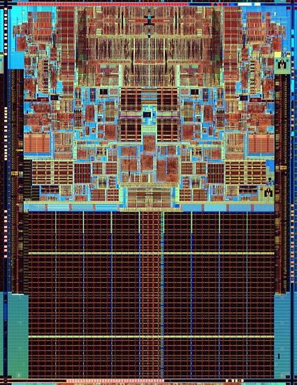
17 Microphotograph of a state-of-the-art CPU chip ecture 07-17

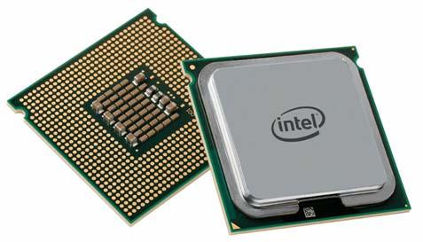
18 Structure of MOSFET Four terminals: Gate, Source, Drain and body Two types n-channel (NMOS) p-channel (PMOS) The minimum alue of is referred as the feature size of the fabrication technology. E.g., 45nm is used for Intel s Core 2 processors. symbol ecture 07-18
 i G =0 (always), i DS = 0 Depletion region between n+ and p-type bulk No current can flow, transistor is said in Cutoff mode ecture")
19 ow Gate Voltage Body is commonly tied to ground When the gate is at a low oltage (V GS ~ 0): P-type body is at low oltage Source-body and drain-body diodes are OFF (reerse bias) i G =0 (always), i DS = 0 Depletion region between n+ and p-type bulk No current can flow, transistor is said in Cutoff mode ecture 07-19
20 Increase Gate Voltage Vertical electric field established Under the gate-oxide: Holes (positie charges) repelled Depletion region under gate oxide formed ecture 07-20
21 Further Increase Gate Voltage Electrons (minorities in the p region) attracted by the electric field towards the gate, and stopped by the gate oxide A n-type inersion layer formed underneath the gate oxide when V GS reaches a certain alue, called threshold oltage (V t, or V TN for NMOS) The channel connects the S and D and now currents can flow between them ecture 07-21

22 inear (Triode) Mode of Operation When GS > V t and a small DS is applied Current flows from D to S (Electrons flow from S to D) i DS DS Increasing GS aboe V t increases the electron density in the channel, and in turn increases the conductiity between D & S Such deices are called enhancement-type MOSFET In this mode, transistor = a oltage controlled resistor ecture 07-22

23 Increase Drain Voltage: Channel Pinch-Off G D S Increase DS Decrease GD less electrons at the drain side of the channel When DS GS V t V GD V t no channel exists at the drain side. The channel pinches-off ecture 07-23
24 Saturation Mode of Operation G D S When channel pinches off, electrons still flows from S to D Electrons are diffused from the channel to the depletion region near D, where they are drifted by the lateral E-field to the D Similar to a reerse-biased B-C junction in a BJT Further increase of DS no effect on the channel current is saturated and the transistor is in Saturation Mode In this mode, transistor = a oltage controlled current source ecture 07-24
25 Qualitatie I-V Characteristic Pinch Off ecture 07-25
26 I-V Characteristics In the inear region, drain current depends on How much charge is in the channel How fast the charge is moing I dq dt = amount of charge in the channel time it takes the carriers to get across the channel ecture 07-26
 Vt 14243 4 ox = ε Aerage gate-channel oltage ox / t ox Ref: G.-Y.")
27 Amount of Channel Charge MOS structure looks like a parallel plate capacitor V GC is composed of two components V t to form the channel (V GC -V t ) to accumulate negatie charges in the channel Q C V channel = ε = V ox GC = CV W t ox V t = C = ox W where C ( GS DS / 2 ) Vt ox = ε Aerage gate-channel oltage ox / t ox Ref: G.-Y. Wei, notes ES154, Harard Uniersity ecture 07-27
28 Charge is carried by electrons. Carrier Velocity Carrier elocity is proportional to the lateral E-field between source and drain = µ ne where µ n is E = / DS Time for carriers to cross the channel is the mobility t = / = = µ E n µ n 2 DS ecture 07-28
29 I-V Behaior: inear Mode Combine the channel charge and elocity to find the current flow Current = amount of charge in the channel / time it takes the carriers to get across the channel i D = Q = µ C = K channel n n t ox ( GS = C W ( V t ox µ n W( GS Vt DS / 2) 2 GS V DS t / 2) / 2) = µ C ( µ C n ox ) is a constant determined by the processing technology, and is denoted by K n W/ is a main design parameter in integrated circuit design. DS DS DS where W 1 2 i D = ( µ ncox ) ( GS Vt ) DS DS 2 K n DS n ox W ecture 07-29
30 I-V Behaior: Saturation Mode If GD V t, channel pinches off near the drain When DS V dsat = GS V t Now, drain oltage no longer increases with DS Putting DS = GS V t to the equation: 1 2 i D independent of DS. W 1 2 i D = ( µ ncox ) ( GS Vt ) DS DS 2 i W 2 for V D = ( µ ncox) ( GS Vt ) GS > V t and V DS GS -V t ecture 07-30
31 Summary of NMOS I-V Characteristics Region Cutoff Triode Saturation Conditions GS < V t DS GS V t V < GS Vt DS GS t I-V relation i D = 0 i D = K ' n W ( GS V ) t DS DS i D = 1 2 K ' n W ( GS V t 2 ) Cutoff region Triode region GS DS < V t GS GS < V t and V t K ' = µ C n n ox Saturation region GS DS V t GS and V t ecture 07-31
32 Ideal Square aw Model: I D s V GS In saturation mode: i D 1 = ( µ nc 2 ox W ) ( GS V ) t 2 MOS s. BJT Current is quadratic with oltage in MOS s. exponential relationship in BJT Saturation mode of MOS corresponds to actie mode of BJT ecture 07-32
33 Ideal Square-aw Model: I D s V DS NMOS ecture 07-33
34 Topics to coer Common-Collector Amplifier MOS Field Effect Transistor Physical Operation and I-V Characteristics of n-channel deices Non-ideal effects P-channel deices and other types ecture 07-34
35 Non-ideal Effects Channel length modulation Body effect Temperature influence Breakdown ecture 07-35


36 Channel-ength Modulation where gate-to-channel oltage = V TN At DS = GS -V TN =V DSsat, Channel pinch-off As DS increases beyond DSsat, the pinch off point moes away from D towards S The effectie channel length is reduced by I D increases An effect similar to Early effect in BJT i D = ' K n W 2 GS V TN 2 ecture 07-36

37 Channel-ength Modulation This effect is modeled by adding a term (1+λ DS ) to the I-V equation: ' K = n W 2 i V 1+ λ D GS TN 2 DS λ = channel length modulation parameter ecture 07-37
 layer = amount of positie charges in the gate (Constant for a fixed gate-source oltage) Channel depth is reduced This is equialent to an increase in the threshold oltage ecture")
38 Body Effect Channel-body can be regarded as a pn junction If channel-body junction is reerse-biased, Depletion layer beneath the gate oxide becomes wider Since the amount of negatie charges in the ( channel + depletion ) layer = amount of positie charges in the gate (Constant for a fixed gate-source oltage) Channel depth is reduced This is equialent to an increase in the threshold oltage ecture 07-38
 (source-body oltage) It follows that the body oltage controls i D. This phenomenon is known as the body effect.")
39 Body Effect Non-zero SB changes threshold oltage: V TN = V + γ + 2φ 2φ TO SB F F where V TO = zero substrate bias for V TN (V) γ= body-effect parameter ( V) 2Φ F = surface potential parameter (V) (source-body oltage) It follows that the body oltage controls i D. This phenomenon is known as the body effect. ecture 07-39
40 Effects of Temperature V t and mobility µ are sensitie to temperature: V t decreases by 2mV for eery 1ºC rise in temperature mobility µ decreases with temperature Oerall, increase in temperature results in lower drain currents ecture 07-40

41 Aalanche Breakdown As V D is increased, the drain-body junction becomes reersed biased Breakdown occurs at oltages of 20 to 150V Rapid increase in the drain current Normally, no permanent damage to the deice ecture 07-41
42 Punch-through Breakdown Whe V D is increased to a point, the depletion region surrounding D extends to the S Punch-through breakdown (about 20 V) Occurs in deices with short channels Normally, no permanent damage to the deice ecture 07-42
43 Gate Oxide Breakdown When V GS exceeds about 30 V (or lower in modern IC technology) Gate oxide breaks down like in the case of a capacitor Results in permanent damage to the deice ecture 07-43
44 Input Protection Input Pin to gates Since the MOSFET has a ery small input capacitance and a ery high input resistance, a small amount of static charges accumulating on the gate can cause the gate oltage to exceed the breakdown leel e.g., Electrostatic Discharge (ESD) from human body Clamping diodes can be used in the I/O pins to protect the circuit from gate-oxide breakdown ecture 07-44
45 Topics to coer Common-Collector Amplifier MOS Field Effect Transistor Physical Operation and I-V Characteristics of n-channel deices Non-ideal effects P-channel deices and other types ecture 07-45
46 P-channel MOSFET (PMOS) Similar to NMOS, but doping and oltages reersed Body tied to highest oltage (Vdd) to preent forward-biasing pn junctions Source typically tied to Vdd too Gate oltage high: transistor is OFF Gate oltage low: transistor is ON when V GS < V t (threshold oltage) Inerted channel of positiely charged holes GS and DS are negatie and V t is also negatie Symbols ecture 07-46
47 PMOS I-V Characteristics Cutoff region GS < Vt V t, GS and DS are negatie. Triode region GS DS V < GS Saturation region GS DS V t t GS and V t and V t i D Cutoff = 0 where K p = K p ' W, i D = K ' = µ C p K p Triode/inear p ox V ( GS t ) DS DS i D = 1 2 K Saturation p ( GS V t 2 ) µ p is 2 or 3-times lower than µ n ecture 07-47

48 Complementary MOS (CMOS) Technology PMOS transistor is fabricated in the n well Complementary MOS or CMOS integrated-circuit technologies proide both NMOS and PMOS on a same IC ecture 07-48
49 Depletion-mode MOSFET A depletion-type MOSFET has a built-in channel by fabrication It is ON when no gate-source oltage is applied Must apply a negatie GS to turn off deice V t is negatie for NMOS enhancement depletion ecture 07-49
50 MOSFET Circuit Symbols (g) and(i) are the most commonly used symbols in VSI logic design. MOS deices are symmetric. In NMOS, n + region at higher oltage is the drain. In PMOS p + region at lower oltage is the drain ecture 07-50
Field-Effect Transistor (FET) is one of the two major transistors; FET derives its name from its working mechanism;
 is one of the two major transistors; FET derives its name from its working mechanism;") Chapter 3 Field-Effect Transistors (FETs) 3.1 Introduction Field-Effect Transistor (FET) is one of the two major transistors; FET derives its name from its working mechanism; The concept has been known
Chapter 3 Field-Effect Transistors (FETs) 3.1 Introduction Field-Effect Transistor (FET) is one of the two major transistors; FET derives its name from its working mechanism; The concept has been known
Electronic Instrumentation Experiment 6 -- Digital Switching
 1 Electronic Instrumentation Experiment 6 -- Digital Switching Part A: Transistor Switches Part B: Comparators and Schmitt Triggers Part C: Digital Switching Part D: Switching a elay Part A: Transistors
ECEN325: Electronics Summer 2018
 ECEN325: Electronics Summer 2018 Metal-Oxide-Semiconductor Field Effect Transistor (MOSFET) Sam Palermo Analog & Mixed-Signal Center Texas A&M University Announcements & Reading H5 due today Exam 2 on
MOS Field Effect Transistors
 MOS Field Effect Transistors A gate contact gate interconnect n polysilicon gate source contacts W active area (thin oxide area) polysilicon gate contact metal interconnect drain contacts A bulk contact
MOSFET in ON State (V GS > V TH )
") ndian nstitute of Technology Jodhpur, Year 08 Analog Electronics (ourse ode: EE34) ecture 8 9: MOSFETs, Biasing ourse nstructor: Shree Prakash Tiwari Email: sptiwari@iitj.ac.in Webpage: http://home.iitj.ac.in/~sptiwari/
ndian nstitute of Technology Jodhpur, Year 08 Analog Electronics (ourse ode: EE34) ecture 8 9: MOSFETs, Biasing ourse nstructor: Shree Prakash Tiwari Email: sptiwari@iitj.ac.in Webpage: http://home.iitj.ac.in/~sptiwari/
Solid State Devices- Part- II. Module- IV
 Solid State Devices- Part- II Module- IV MOS Capacitor Two terminal MOS device MOS = Metal- Oxide- Semiconductor MOS capacitor - the heart of the MOSFET The MOS capacitor is used to induce charge at the
ECE520 VLSI Design. Lecture 2: Basic MOS Physics. Payman Zarkesh-Ha
 ECE520 VLSI Design Lecture 2: Basic MOS Physics Payman Zarkesh-Ha Office: ECE Bldg. 230B Office hours: Wednesday 2:00-3:00PM or by appointment E-mail: pzarkesh@unm.edu Slide: 1 Review of Last Lecture Semiconductor
INTRODUCTION: Basic operating principle of a MOSFET:
 INTRODUCTION: Along with the Junction Field Effect Transistor (JFET), there is another type of Field Effect Transistor available whose Gate input is electrically insulated from the main current carrying
UNIVERSITY OF CALIFORNIA AT BERKELEY College of Engineering Department of Electrical Engineering and Computer Sciences.
 UNIVERSITY OF CALIFORNIA AT BERKELEY College of Engineering Department of Electrical Engineering and Computer Sciences Discussion #9 EE 05 Spring 2008 Prof. u MOSFETs The standard MOSFET structure is shown
EE301 Electronics I , Fall
 EE301 Electronics I 2018-2019, Fall 1. Introduction to Microelectronics (1 Week/3 Hrs.) Introduction, Historical Background, Basic Consepts 2. Rewiev of Semiconductors (1 Week/3 Hrs.) Semiconductor materials
Course Outline. 4. Chapter 5: MOS Field Effect Transistors (MOSFET) 5. Chapter 6: Bipolar Junction Transistors (BJT)
 5. Chapter 6: Bipolar Junction Transistors (BJT)") Course Outline 1. Chapter 1: Signals and Amplifiers 1 2. Chapter 3: Semiconductors 3. Chapter 4: Diodes 4. Chapter 5: MOS Field Effect Transistors (MOSFET) 5. Chapter 6: Bipolar Junction Transistors (BJT)
Course Outline 1. Chapter 1: Signals and Amplifiers 1 2. Chapter 3: Semiconductors 3. Chapter 4: Diodes 4. Chapter 5: MOS Field Effect Transistors (MOSFET) 5. Chapter 6: Bipolar Junction Transistors (BJT)
UNIT-1 Bipolar Junction Transistors. Text Book:, Microelectronic Circuits 6 ed., by Sedra and Smith, Oxford Press
 UNIT-1 Bipolar Junction Transistors Text Book:, Microelectronic Circuits 6 ed., by Sedra and Smith, Oxford Press Figure 6.1 A simplified structure of the npn transistor. Microelectronic Circuits, Sixth
MOS Field-Effect Transistors (MOSFETs)
") 6 MOS Field-Effect Transistors (MOSFETs) A three-terminal device that uses the voltages of the two terminals to control the current flowing in the third terminal. The basis for amplifier design. The basis
6 MOS Field-Effect Transistors (MOSFETs) A three-terminal device that uses the voltages of the two terminals to control the current flowing in the third terminal. The basis for amplifier design. The basis
Design cycle for MEMS
 Design cycle for MEMS Design cycle for ICs IC Process Selection nmos CMOS BiCMOS ECL for logic for I/O and driver circuit for critical high speed parts of the system The Real Estate of a Wafer MOS Transistor
MOSFET Terminals. The voltage applied to the GATE terminal determines whether current can flow between the SOURCE & DRAIN terminals.
 MOSFET Terminals The voltage applied to the GATE terminal determines whether current can flow between the SOURCE & DRAIN terminals. For an n-channel MOSFET, the SOURCE is biased at a lower potential (often
UNIT 3: FIELD EFFECT TRANSISTORS
 FIELD EFFECT TRANSISTOR: UNIT 3: FIELD EFFECT TRANSISTORS The field effect transistor is a semiconductor device, which depends for its operation on the control of current by an electric field. There are
Laboratory #5 BJT Basics and MOSFET Basics
 Laboratory #5 BJT Basics and MOSFET Basics I. Objectives 1. Understand the physical structure of BJTs and MOSFETs. 2. Learn to measure I-V characteristics of BJTs and MOSFETs. II. Components and Instruments
BJT Amplifier. Superposition principle (linear amplifier)
") BJT Amplifier Two types analysis DC analysis Applied DC voltage source AC analysis Time varying signal source Superposition principle (linear amplifier) The response of a linear amplifier circuit excited
BJT Amplifier Two types analysis DC analysis Applied DC voltage source AC analysis Time varying signal source Superposition principle (linear amplifier) The response of a linear amplifier circuit excited
Lecture-45. MOS Field-Effect-Transistors Threshold voltage
 Lecture-45 MOS Field-Effect-Transistors 7.4. Threshold voltage In this section we summarize the calculation of the threshold voltage and discuss the dependence of the threshold voltage on the bias applied
MOSFET Common Source Amplifier
 Microelectronic Circuits MOSFET Common Source Amplifier Slide 1 Small nal Model The definition of Transconductance g m i D S S S k n W L O The definition of output resistance r o DS I The definition of
ELG 2135 ELECTRONICS I FOURTH CHAPTER : BIPOLAR JUNCTION TRANSISTORS
 ELG 2135 ELECTRONICS I FOURTH CHAPTER : BIPOLAR JUNCTION TRANSISTORS Session WINTER 2003 Dr M. YAGOUB Fourth Chapter: Bipolar Junction Transistors IV - 2 _ Haing studied the junction diode, which is the
Difference between BJTs and FETs. Junction Field Effect Transistors (JFET)
") Difference between BJTs and FETs Transistors can be categorized according to their structure, and two of the more commonly known transistor structures, are the BJT and FET. The comparison between BJTs
Difference between BJTs and FETs Transistors can be categorized according to their structure, and two of the more commonly known transistor structures, are the BJT and FET. The comparison between BJTs
I E I C since I B is very small
 Figure 2: Symbols and nomenclature of a (a) npn and (b) pnp transistor. The BJT consists of three regions, emitter, base, and collector. The emitter and collector are usually of one type of doping, while
MEASUREMENT AND INSTRUMENTATION STUDY NOTES UNIT-I
 MEASUREMENT AND INSTRUMENTATION STUDY NOTES The MOSFET The MOSFET Metal Oxide FET UNIT-I As well as the Junction Field Effect Transistor (JFET), there is another type of Field Effect Transistor available
UNIT 3 Transistors JFET
 UNIT 3 Transistors JFET Mosfet Definition of BJT A bipolar junction transistor is a three terminal semiconductor device consisting of two p-n junctions which is able to amplify or magnify a signal. It
Field Effect Transistors
 Field Effect Transistors LECTURE NO. - 41 Field Effect Transistors www.mycsvtunotes.in JFET MOSFET CMOS Field Effect transistors - FETs First, why are we using still another transistor? BJTs had a small
Department of Electrical Engineering IIT Madras
 Department of Electrical Engineering IIT Madras Sample Questions on Semiconductor Devices EE3 applicants who are interested to pursue their research in microelectronics devices area (fabrication and/or
SAMPLE FINAL EXAMINATION FALL TERM
 ENGINEERING SCIENCES 154 ELECTRONIC DEVICES AND CIRCUITS SAMPLE FINAL EXAMINATION FALL TERM 2001-2002 NAME Some Possible Solutions a. Please answer all of the questions in the spaces provided. If you need
55:041 Electronic Circuits
 55:041 Electronic Circuits Mosfet Review Sections of Chapter 3 &4 A. Kruger Mosfet Review, Page-1 Basic Structure of MOS Capacitor Sect. 3.1 Width 1 10-6 m or less Thickness 50 10-9 m or less ` MOS Metal-Oxide-Semiconductor
Lecture 26 Differential Amplifiers (I) DIFFERENTIAL AMPLIFIERS
 DIFFERENTIAL AMPLIFIERS") Lecture 6 Differential Amplifiers (I) DIFFERENTIAL AMPLIFIERS Outline 1. Introduction. Incremental analysis of differential amplifier 3. Common-source differential amplifier Reading Assignment: Howe and
Lecture 6 Differential Amplifiers (I) DIFFERENTIAL AMPLIFIERS Outline 1. Introduction. Incremental analysis of differential amplifier 3. Common-source differential amplifier Reading Assignment: Howe and
97.398*, Physical Electronics, Lecture 21. MOSFET Operation
 97.398*, Physical Electronics, Lecture 21 MOSFET Operation Lecture Outline Last lecture examined the MOSFET structure and required processing steps Now move on to basic MOSFET operation, some of which
Chapter 6: Field-Effect Transistors
 Chapter 6: Field-Effect Transistors FETs vs. BJTs Similarities: Amplifiers Switching devices Impedance matching circuits Differences: FETs are voltage controlled devices. BJTs are current controlled devices.
EE70 - Intro. Electronics
 EE70 - Intro. Electronics Course website: ~/classes/ee70/fall05 Today s class agenda (November 28, 2005) review Serial/parallel resonant circuits Diode Field Effect Transistor (FET) f 0 = Qs = Qs = 1 2π
Lecture 1. EE 215 Electronic Devices & Circuits. Semiconductor Devices: Diodes. The Ideal Diode
 Lecture 1 EE 215 Electronic Deices & Circuits Asst Prof Muhammad Anis Chaudhary EE 215 Electronic Deices & Circuits Credit Hours: 3 1 Course Book: Adel S. Sedra and Kenneth C. Smith, Microelectronic Circuits,
Metal-Oxide-Silicon (MOS) devices PMOS. n-type
 devices PMOS. n-type") Metal-Oxide-Silicon (MOS devices Principle of MOS Field Effect Transistor transistor operation Metal (poly gate on oxide between source and drain Source and drain implants of opposite type to substrate.
Metal-Oxide-Silicon (MOS devices Principle of MOS Field Effect Transistor transistor operation Metal (poly gate on oxide between source and drain Source and drain implants of opposite type to substrate.
EE 171. MOS Transistors (Chapter 5) University of California, Santa Cruz May 1, 2007
 University of California, Santa Cruz May 1, 2007") EE 171 MOS Transistors (Chapter 5) Uniersity of California, Santa Cruz May 1, 007 FET: Fiel Effect Transistors MOSFET (Metal-Oxie-Semiconuctor) N-channel (NMOS) P-channel (PMOS) Enhancement type (V to
EE 171 MOS Transistors (Chapter 5) Uniersity of California, Santa Cruz May 1, 007 FET: Fiel Effect Transistors MOSFET (Metal-Oxie-Semiconuctor) N-channel (NMOS) P-channel (PMOS) Enhancement type (V to
EE105 Fall 2015 Microelectronic Devices and Circuits
 EE105 Fall 2015 Microelectronic Devices and Circuits Prof. Ming C. Wu wu@eecs.berkeley.edu 511 Sutardja Dai Hall (SDH) 11-1 Transistor Operating Mode in Amplifiers Transistors are biased in flat part of
Q1. Explain the construction and principle of operation of N-Channel and P-Channel Junction Field Effect Transistor (JFET).
.") Q. Explain the construction and principle of operation of N-Channel and P-Channel Junction Field Effect Transistor (JFET). Answer: N-Channel Junction Field Effect Transistor (JFET) Construction: Drain(D)
Q. Explain the construction and principle of operation of N-Channel and P-Channel Junction Field Effect Transistor (JFET). Answer: N-Channel Junction Field Effect Transistor (JFET) Construction: Drain(D)
F7 Transistor Amplifiers
 Lars Ohlsson 2018-09-25 F7 Transistor Amplifiers Outline Transfer characteristics Small signal operation and models Basic configurations Common source (CS) CS/CE w/ source/ emitter degeneration resistance
MOSFET & IC Basics - GATE Problems (Part - I)
") MOSFET & IC Basics - GATE Problems (Part - I) 1. Channel current is reduced on application of a more positive voltage to the GATE of the depletion mode n channel MOSFET. (True/False) [GATE 1994: 1 Mark]
MOSFET & IC Basics - GATE Problems (Part - I) 1. Channel current is reduced on application of a more positive voltage to the GATE of the depletion mode n channel MOSFET. (True/False) [GATE 1994: 1 Mark]
Advanced Test Equipment Rentals ATEC (2832)
") Established 1981 Adanced Test Equipment Rentals www.atecorp.com 800-404-ATEC (2832) UNIVERSITY OF UTAH ELECTRICAL AND COMPUTER ENGINEERING DEPARTMENT ANALOG INTEGRATED CIRCUITS LAB LAB 5 Two-Stage CMOS
Established 1981 Adanced Test Equipment Rentals www.atecorp.com 800-404-ATEC (2832) UNIVERSITY OF UTAH ELECTRICAL AND COMPUTER ENGINEERING DEPARTMENT ANALOG INTEGRATED CIRCUITS LAB LAB 5 Two-Stage CMOS
Session 10: Solid State Physics MOSFET
 Session 10: Solid State Physics MOSFET 1 Outline A B C D E F G H I J 2 MOSCap MOSFET Metal-Oxide-Semiconductor Field-Effect Transistor: Al (metal) SiO2 (oxide) High k ~0.1 ~5 A SiO2 A n+ n+ p-type Si (bulk)
1 Introduction to analog CMOS design
 1 Introduction to analog CMOS design This chapter begins by explaining briefly why there is still a need for analog design and introduces its main tradeoffs. The need for accurate component modeling follows.
Unit III FET and its Applications. 2 Marks Questions and Answers
 Unit III FET and its Applications 2 Marks Questions and Answers 1. Why do you call FET as field effect transistor? The name field effect is derived from the fact that the current is controlled by an electric
Introduction to MOSFET MOSFET (Metal Oxide Semiconductor Field Effect Transistor)
") Microelectronic Circuits Introduction to MOSFET MOSFET (Metal Oxide Semiconductor Field Effect Transistor) Slide 1 MOSFET Construction MOSFET (Metal Oxide Semiconductor Field Effect Transistor) Slide 2
Microelectronic Circuits Introduction to MOSFET MOSFET (Metal Oxide Semiconductor Field Effect Transistor) Slide 1 MOSFET Construction MOSFET (Metal Oxide Semiconductor Field Effect Transistor) Slide 2
Chapter 6: Operational Amplifier (Op Amp)
") Chapter 6: Operational Amplifier (Op Amp) 6.1 What is an Op Amp? 6.2 Ideal Op Amp 6.3 Nodal Analysis of Circuits with Op Amps 6.4 Configurations of Op Amp 6.5 Cascaded Op Amp 6.6 Op Amp Circuits & Linear
Chapter 6: Operational Amplifier (Op Amp) 6.1 What is an Op Amp? 6.2 Ideal Op Amp 6.3 Nodal Analysis of Circuits with Op Amps 6.4 Configurations of Op Amp 6.5 Cascaded Op Amp 6.6 Op Amp Circuits & Linear
Field Effect Transistors (FET s) University of Connecticut 136
 University of Connecticut 136") Field Effect Transistors (FET s) University of Connecticut 136 Field Effect Transistors (FET s) FET s are classified three ways: by conduction type n-channel - conduction by electrons p-channel - conduction
Field Effect Transistors (FET s) University of Connecticut 136 Field Effect Transistors (FET s) FET s are classified three ways: by conduction type n-channel - conduction by electrons p-channel - conduction
Physics 364, Fall 2012, reading due your answers to by 11pm on Thursday
 Physics 364, Fall 2012, reading due 2012-10-25. Email your answers to ashmansk@hep.upenn.edu by 11pm on Thursday Course materials and schedule are at http://positron.hep.upenn.edu/p364 Assignment: (a)
EE 5611 Introduction to Microelectronic Technologies Fall Thursday, September 04, 2014 Lecture 02
 EE 5611 Introduction to Microelectronic Technologies Fall 2014 Thursday, September 04, 2014 Lecture 02 1 Lecture Outline Review on semiconductor materials Review on microelectronic devices Example of microelectronic
NAME: Last First Signature
 UNIVERSITY OF CALIFORNIA, BERKELEY College of Engineering Department of Electrical Engineering and Computer Sciences EE 130: IC Devices Spring 2003 FINAL EXAMINATION NAME: Last First Signature STUDENT
MTLE-6120: Advanced Electronic Properties of Materials. Semiconductor transistors for logic and memory. Reading: Kasap
 MTLE-6120: Advanced Electronic Properties of Materials 1 Semiconductor transistors for logic and memory Reading: Kasap 6.6-6.8 Vacuum tube diodes 2 Thermionic emission from cathode Electrons collected
Lecture 16: MOS Transistor models: Linear models, SPICE models. Context. In the last lecture, we discussed the MOS transistor, and
 Lecture 16: MOS Transistor models: Linear models, SPICE models Context In the last lecture, we discussed the MOS transistor, and added a correction due to the changing depletion region, called the body
Lecture 3: Transistors
 Lecture 3: Transistors Now that we know about diodes, let s put two of them together, as follows: collector base emitter n p n moderately doped lightly doped, and very thin heavily doped At first glance,
EE105 Fall 2015 Microelectronic Devices and Circuits: MOSFET Prof. Ming C. Wu 511 Sutardja Dai Hall (SDH)
") EE105 Fall 2015 Microelectronic Devices and Circuits: MOSFET Prof. Ming C. Wu wu@eecs.berkeley.edu 511 Sutardja Dai Hall (SDH) 7-1 Simplest Model of MOSFET (from EE16B) 7-2 CMOS Inverter 7-3 CMOS NAND
EE105 Fall 2015 Microelectronic Devices and Circuits: MOSFET Prof. Ming C. Wu wu@eecs.berkeley.edu 511 Sutardja Dai Hall (SDH) 7-1 Simplest Model of MOSFET (from EE16B) 7-2 CMOS Inverter 7-3 CMOS NAND
EE5320: Analog IC Design
 EE5320: Analog IC Design Handout 3: MOSFETs Saurabh Saxena & Qadeer Khan Indian Institute of Technology Madras Copyright 2018 by EE6:Integrated Circuits & Systems roup @ IIT Madras Overview Transistors
EJERCICIOS DE COMPONENTES ELECTRÓNICOS. 1 er cuatrimestre
 EJECICIOS DE COMPONENTES ELECTÓNICOS. 1 er cuatrimestre 2 o Ingeniería Electrónica Industrial Juan Antonio Jiménez Tejada Índice 1. Basic concepts of Electronics 1 2. Passive components 1 3. Semiconductors.
Week 12: Output Stages, Frequency Response
 ELE 2110A Electronic Circuits Week 12: Output Stages, Frequency esponse (2 hours only) Lecture 12-1 Output Stages Topics to cover Amplifier Frequency esponse eading Assignment: Chap 15.3, 16.1 of Jaeger
Session 2 MOS Transistor for RF Circuits
 Session 2 MOS Transistor for RF Circuits Session Speaker Chandramohan P. Session Contents MOS transistor basics MOS equivalent circuit Single stage amplifiers Opamp design Session objectives To understand
Chapter 4. CMOS Cascode Amplifiers. 4.1 Introduction. 4.2 CMOS Cascode Amplifiers
 Chapter 4 CMOS Cascode Amplifiers 4.1 Introduction A single stage CMOS amplifier cannot give desired dc voltage gain, output resistance and transconductance. The voltage gain can be made to attain higher
MOSFET Amplifier Configuration. MOSFET Amplifier Configuration
 MOSFET Amplifier Configuration Single stage The signal is fed to the amplifier represented as sig with an internal resistance sig. MOSFET is represented by its small signal model. Generally interested
Bipolar Junction Transistor (BJT) Basics- GATE Problems
 Basics- GATE Problems") Bipolar Junction Transistor (BJT) Basics- GATE Problems One Mark Questions 1. The break down voltage of a transistor with its base open is BV CEO and that with emitter open is BV CBO, then (a) BV CEO =
Bipolar Junction Transistor (BJT) Basics- GATE Problems One Mark Questions 1. The break down voltage of a transistor with its base open is BV CEO and that with emitter open is BV CBO, then (a) BV CEO =
8. Characteristics of Field Effect Transistor (MOSFET)
") 1 8. Characteristics of Field Effect Transistor (MOSFET) 8.1. Objectives The purpose of this experiment is to measure input and output characteristics of n-channel and p- channel field effect transistors
1 8. Characteristics of Field Effect Transistor (MOSFET) 8.1. Objectives The purpose of this experiment is to measure input and output characteristics of n-channel and p- channel field effect transistors
Device Technologies. Yau - 1
 Device Technologies Yau - 1 Objectives After studying the material in this chapter, you will be able to: 1. Identify differences between analog and digital devices and passive and active components. Explain
Chapter 2 : Semiconductor Materials & Devices (II) Feb
 Feb") Chapter 2 : Semiconductor Materials & Devices (II) 1 Reference 1. SemiconductorManufacturing Technology: Michael Quirk and Julian Serda (2001) 3. Microelectronic Circuits (5/e): Sedra & Smith (2004) 4.
Chapter 2 : Semiconductor Materials & Devices (II) 1 Reference 1. SemiconductorManufacturing Technology: Michael Quirk and Julian Serda (2001) 3. Microelectronic Circuits (5/e): Sedra & Smith (2004) 4.
Circuit produces an amplified negative version of v IN = R R R
 Inerting Amplifier Circuit produces an amplified negatie ersion of i = i, = 2 0 = 2 OUT OUT = 2 Example: Calculate OUT / and I for = 0.5V Solution: A V OUT 2 = = = 0 kω = 0 kω i 05. V = = = kω 05. ma
6.012 Microelectronic Devices and Circuits
 Page 1 of 13 YOUR NAME Department of Electrical Engineering and Computer Science Massachusetts Institute of Technology 6.012 Microelectronic Devices and Circuits Final Eam Closed Book: Formula sheet provided;
Georgia Institute of Technology School of Electrical and Computer Engineering. Midterm Exam
 Georgia Institute of Technology School of Electrical and Computer Engineering Midterm Exam ECE-3400 Fall 2013 Tue, September 24, 2013 Duration: 80min First name Solutions Last name Solutions ID number
Microelectronics Circuit Analysis and Design. MOS Capacitor Under Bias: Electric Field and Charge. Basic Structure of MOS Capacitor 9/25/2013
 Microelectronics Circuit Analysis and Design Donald A. Neamen Chapter 3 The Field Effect Transistor In this chapter, we will: Study and understand the operation and characteristics of the various types
55:041 Electronic Circuits
 55:041 Electronic Circuits MOSFETs Sections of Chapter 3 &4 A. Kruger MOSFETs, Page-1 Basic Structure of MOS Capacitor Sect. 3.1 Width = 1 10-6 m or less Thickness = 50 10-9 m or less ` MOS Metal-Oxide-Semiconductor
MOS TRANSISTOR THEORY
 MOS TRANSISTOR THEORY Introduction A MOS transistor is a majority-carrier device, in which the current in a conducting channel between the source and the drain is modulated by a voltage applied to the
COMPARISON OF THE MOSFET AND THE BJT:
 COMPARISON OF THE MOSFET AND THE BJT: In this section we present a comparison of the characteristics of the two major electronic devices: the MOSFET and the BJT. To facilitate this comparison, typical
Module-3: Metal Oxide Semiconductor (MOS) & Emitter coupled logic (ECL) families
 & Emitter coupled logic (ECL) families") 1 Module-3: Metal Oxide Semiconductor (MOS) & Emitter coupled logic (ECL) families 1. Introduction 2. Metal Oxide Semiconductor (MOS) logic 2.1. Enhancement and depletion mode 2.2. NMOS and PMOS inverter
1 Module-3: Metal Oxide Semiconductor (MOS) & Emitter coupled logic (ECL) families 1. Introduction 2. Metal Oxide Semiconductor (MOS) logic 2.1. Enhancement and depletion mode 2.2. NMOS and PMOS inverter
Crossover Distortion FETS Spec sheets Configurations Applications
 Crossoer Distortion FETS Spec sheets Configurations Applications Acknowledgements: Neamen, Donald: Microelectronics Circuit Analysis and Design, 3 rd Edition 6.101 Spring 2017 Lecture 6 1 Three Stage Amplifer
Chapter 5: Field Effect Transistors
 Chapter 5: Field Effect Transistors Slide 1 FET FET s (Field Effect Transistors) are much like BJT s (Bipolar Junction Transistors). Similarities: Amplifiers Switching devices Impedance matching circuits
Three Terminal Devices
 Three Terminal Devices - field effect transistor (FET) - bipolar junction transistor (BJT) - foundation on which modern electronics is built - active devices - devices described completely by considering
Field Effect Transistors
 Chapter 5: Field Effect Transistors Slide 1 FET FET s (Field Effect Transistors) are much like BJT s (Bipolar Junction Transistors). Similarities: Amplifiers Switching devices Impedance matching circuits
Experiment 3. 3 MOSFET Drain Current Modeling. 3.1 Summary. 3.2 Theory. ELEC 3908 Experiment 3 Student#:
 Experiment 3 3 MOSFET Drain Current Modeling 3.1 Summary In this experiment I D vs. V DS and I D vs. V GS characteristics are measured for a silicon MOSFET, and are used to determine the parameters necessary
Student Lecture by: Giangiacomo Groppi Joel Cassell Pierre Berthelot September 28 th 2004
 Student Lecture by: Giangiacomo Groppi Joel Cassell Pierre Berthelot September 28 th 2004 Lecture outline Historical introduction Semiconductor devices overview Bipolar Junction Transistor (BJT) Field
Conduction Characteristics of MOS Transistors (for fixed Vds)! Topic 2. Basic MOS theory & SPICE simulation. MOS Transistor
! Topic 2. Basic MOS theory & SPICE simulation. MOS Transistor") Conduction Characteristics of MOS Transistors (for fixed Vds)! Topic 2 Basic MOS theory & SPICE simulation Peter Cheung Department of Electrical & Electronic Engineering Imperial College London (Weste&Harris,
Conduction Characteristics of MOS Transistors (for fixed Vds)! Topic 2 Basic MOS theory & SPICE simulation Peter Cheung Department of Electrical & Electronic Engineering Imperial College London (Weste&Harris,
Topic 2. Basic MOS theory & SPICE simulation
 Topic 2 Basic MOS theory & SPICE simulation Peter Cheung Department of Electrical & Electronic Engineering Imperial College London (Weste&Harris, Ch 2 & 5.1-5.3 Rabaey, Ch 3) URL: www.ee.ic.ac.uk/pcheung/
Conduction Characteristics of MOS Transistors (for fixed Vds) Topic 2. Basic MOS theory & SPICE simulation. MOS Transistor
 Topic 2. Basic MOS theory & SPICE simulation. MOS Transistor") Conduction Characteristics of MOS Transistors (for fixed Vds) Topic 2 Basic MOS theory & SPICE simulation Peter Cheung Department of Electrical & Electronic Engineering Imperial College London (Weste&Harris,
Conduction Characteristics of MOS Transistors (for fixed Vds) Topic 2 Basic MOS theory & SPICE simulation Peter Cheung Department of Electrical & Electronic Engineering Imperial College London (Weste&Harris,
EE 330 Laboratory 7 MOSFET Device Experimental Characterization and Basic Applications Spring 2017
 EE 330 Laboratory 7 MOSFET Device Experimental Characterization and Basic Applications Spring 2017 Objective: The objective of this laboratory experiment is to become more familiar with the operation of
Shorthand Notation for NMOS and PMOS Transistors
 Shorthand Notation for NMOS and PMOS Transistors Terminal Voltages Mode of operation depends on V g, V d, V s V gs = V g V s V gd = V g V d V ds = V d V s = V gs - V gd Source and drain are symmetric diffusion
Lecture 4. MOS transistor theory
 Lecture 4 MOS transistor theory 1.7 Introduction: A MOS transistor is a majority-carrier device, in which the current in a conducting channel between the source and the drain is modulated by a voltage
Learning Outcomes. Spiral 2-6. Current, Voltage, & Resistors DIODES
 26.1 26.2 Learning Outcomes Spiral 26 Semiconductor Material MOS Theory I underst why a diode conducts current under forward bias but does not under reverse bias I underst the three modes of operation
UNIT-VI FIELD EFFECT TRANSISTOR. 1. Explain about the Field Effect Transistor and also mention types of FET s.
 UNIT-I FIELD EFFECT TRANSISTOR 1. Explain about the Field Effect Transistor and also mention types of FET s. The Field Effect Transistor, or simply FET however, uses the voltage that is applied to their
Bipolar Junction Transistors (BJTs) Overview
 Overview") 1 Bipolar Junction Transistors (BJTs) Asst. Prof. MONTREE SIRIPRUCHYANUN, D. Eng. Dept. of Teacher Training in Electrical Engineering, Faculty of Technical Education King Mongkut s Institute of Technology
1 Bipolar Junction Transistors (BJTs) Asst. Prof. MONTREE SIRIPRUCHYANUN, D. Eng. Dept. of Teacher Training in Electrical Engineering, Faculty of Technical Education King Mongkut s Institute of Technology
QUESTION BANK for Analog Electronics 4EC111 *
 OpenStax-CNX module: m54983 1 QUESTION BANK for Analog Electronics 4EC111 * Bijay_Kumar Sharma This work is produced by OpenStax-CNX and licensed under the Creative Commons Attribution License 4.0 Abstract
Chapter Goal. Zulfiqar Ali
 Chapter Goal Understand behaior and characteristics of ideal differential and op amps. Demonstrate circuit analysis techniques for ideal op amps. Characterize inerting, non-inerting, summing and instrumentation
Multistage Amplifiers
 Multistage Amplifiers Single-stage transistor amplifiers are inadequate for meeting most design requirements for any of the four amplifier types (voltage, current, transconductance, and transresistance.)
EIE209 Basic Electronics. Transistor Devices. Contents BJT and FET Characteristics Operations. Prof. C.K. Tse: T ransistor devices
 EIE209 Basic Electronics Transistor Devices Contents BJT and FET Characteristics Operations 1 What is a transistor? Three-terminal device whose voltage-current relationship is controlled by a third voltage
EEEE 381 Electronics I
 EEEE 381 Electronics I Lab #5: Two-Stage CMOS Op-Amp Oeriew In this lab we will expand on the work done in Lab #4, which introduced the actiely-loaded differential pair. A second stage that is comprised
Depletion-mode operation ( 공핍형 ): Using an input gate voltage to effectively decrease the channel size of an FET
: Using an input gate voltage to effectively decrease the channel size of an FET") Ch. 13 MOSFET Metal-Oxide-Semiconductor Field-Effect Transistor : I D D-mode E-mode V g The gate oxide is made of dielectric SiO 2 with e = 3.9 Depletion-mode operation ( 공핍형 ): Using an input gate voltage
Ch. 13 MOSFET Metal-Oxide-Semiconductor Field-Effect Transistor : I D D-mode E-mode V g The gate oxide is made of dielectric SiO 2 with e = 3.9 Depletion-mode operation ( 공핍형 ): Using an input gate voltage
ECEG 350 Electronics I Fall 2017
 EEG 350 Electronics Fall 07 Final Exam General nformation Rough breakdown of topic coverage: 0-0% JT fundamentals and regions of operation 0-40% MOSFET fundamentals biasing and small-signal modeling 0-5%
ECE 546 Lecture 12 Integrated Circuits
 ECE 546 Lecture 12 Integrated Circuits Spring 2018 Jose E. Schutt-Aine Electrical & Computer Engineering University of Illinois jesa@illinois.edu ECE 546 Jose Schutt Aine 1 Integrated Circuits IC Requirements
COLLECTOR DRAIN BASE GATE EMITTER. Applying a voltage to the Gate connection allows current to flow between the Drain and Source connections.
 MOSFETS Although the base current in a transistor is usually small (< 0.1 ma), some input devices (e.g. a crystal microphone) may be limited in their output. In order to overcome this, a Field Effect Transistor
Today s subject MOSFET and IGBT
 Today s subject MOSFET and IGBT 2018-05-22 MOSFET metal oxide semiconductor field effect transistor Drain Gate n-channel Source p-channel The MOSFET - Source Gate G D n + p p n + S body body n - drift
Chapter 5. Operational Amplifiers and Source Followers. 5.1 Operational Amplifier
 Chapter 5 Operational Amplifiers and Source Followers 5.1 Operational Amplifier In single ended operation the output is measured with respect to a fixed potential, usually ground, whereas in double-ended
EE 434 Lecture 21. MOS Amplifiers Bipolar Devices
 434 ecture MOS Amplifiers ipolar Devices Quiz 3 The quiescent voltage across the 5K resistor in the circuit shown was measured to be 3. ) Determine the quiescent output voltage ) Determine the small signal
Integrated Circuit Amplifiers. Comparison of MOSFETs and BJTs
 Integrated Circuit Amplifiers Comparison of MOSFETs and BJTs 17 Typical CMOS Device Parameters 0.8 µm 0.25 µm 0.13 µm Parameter NMOS PMOS NMOS PMOS NMOS PMOS t ox (nm) 15 15 6 6 2.7 2.7 C ox (ff/µm 2 )