Electronic Circuits. Junction Field-effect Transistors. Dr. Manar Mohaisen Office: F208 Department of EECE
|
|
|
- Sara Ellis
- 5 years ago
- Views:
Transcription

1 Electronic Circuits Junction Field-effect Transistors Dr. Manar Mohaisen Office: F208 Department of EECE
2 Review of the Precedent Lecture Explain the Operation Class A Power Amplifier Explain the Operation of Class B and AB Amplifiers Explain The Operation of the Class C Amplifiers
3 Class Objectives Introduce the Junction Field-effect Transistor (JFET) Structure, characteristics and parameters, and biasing Introduce the Metal Oxide Semiconductor FET (MOSFET) Types, characteristics, power MOSFET, and biasing

4 JFET Two Types: n channel and p channel Junction Field-effect Transistor (JFET) The leads are connected to each end of the channel Drain: Connected to the upper end of the channel Source: Connected to the lower end of the channel In case of n channel JFET Two p-type regions are diffused in the n-type material to form a channel. In case of p channel JFET, two n-type regions are used.
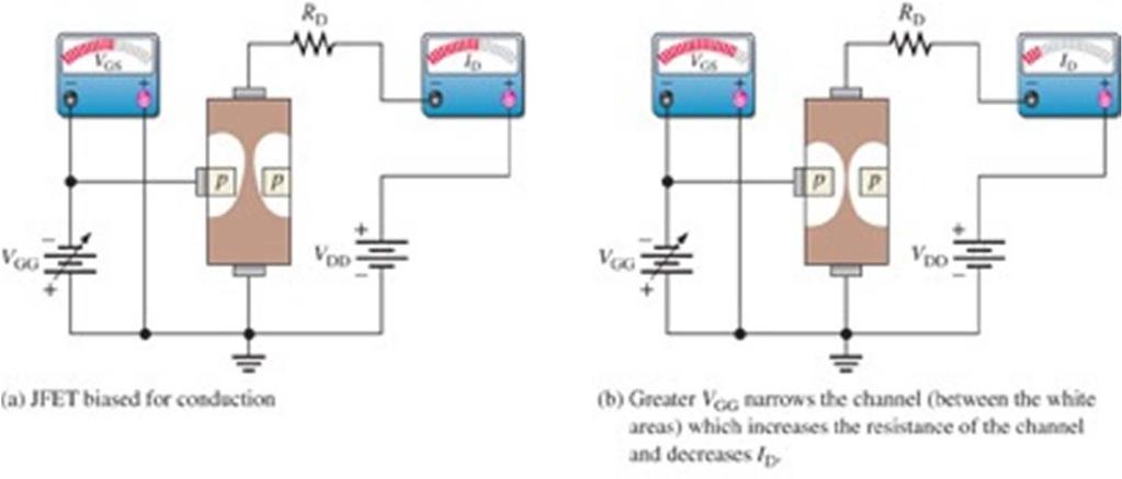
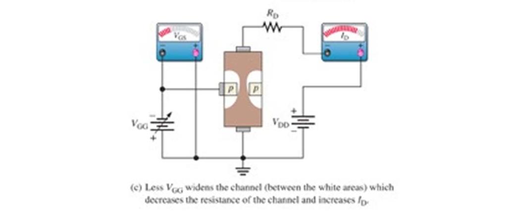
5 Junction Field-effect Transistor (JFET) contd. Basic Operation V DD provides drain-to-source voltage. V GG sets the reverse-bias voltage between the gate and source. JFET is always operated with the gate-source junction reverse-biased.
6 Junction Field-effect Transistor (JFET) contd.
7 JFET Characteristics and Parameters Zero V GG Ohmic Region When V DS increases, I D will increase proportionally. Channel resistance is essentially constant. Active Region I D becomes essentially constant. Starting at the Pinch-Off Voltage, V p. V GD increases and creates a depletion region that offsets the increase in V GS.
8 JFET Characteristics and Parameters contd. Zero V GG contd. Breakdown The point at which I D starts to increase very rapidly with any increase in V DS. Usual Operation of the JFET In the active region.
9 JFET Characteristics and Parameters contd. V GS Controls I D I D decreases as the value of V GS increases. The depletion region is increased and the channel is narrowed.
.")
10 JFET Characteristics and Parameters contd. Cutoff Voltage The value of V GS that makes I D approximately zero. Therefore, the JFET must be operated Between V GS = 0 V and V GS(off). I D will, therefore, vary between I DSS (max value) and zero.
11 JFET Characteristics and Parameters contd. Remarks The pinch-off voltage Vp is measured when V GS = 0. I D starts to be constant. I D is maximum and equals to I DSS. The pinch-off occurs for any value of V GS (less than 0) I D starts to be constant. I D is less than I DSS. V DS is less than Vp. Cutoff Voltage and Pinch-off voltage They are equal in magnitude and opposite in sign.
12 Example 8-1 V GS(off) = -4 V and I DSS = 12 ma. JFET Characteristics and Parameters contd. Determine the minimum value of V DD to put the device in the constant-current region of operation when V GS = 0V. V DS = V P = - V GS(off) = 4 V. I 12 ma D = IDSS = V = I R = (12mA)(560 Ω ) = 6.72 V R D D D V = 4 V 6.72V V DD V + DS V = + = R D
13 JFET Universal Transfer Characteristic Transconductance curve. JFET Characteristics and Parameters contd. I = 0, when V = V D GS GS GS(off) I I = DSS, when V = 0.5V D 4 GS I I = DSS, when V = 0.3V D 2 GS and I = I, when V = 0 D DSS GS(off) GS(off)
14 JFET Characteristics and Parameters contd. Characteristic Curve It is expressed approximately by I D I DSS 1 V 2 VGS GS(off) JFETs and MOSFETs are known as square-law devices
15 The Forward Transconductance JFET Characteristics and Parameters contd. The change in drain current for a given change in gate-to-source voltage. ΔI g D m = Δ V GS g m m0 = g 1 V VGS GS(off) g m0 2I = V DSS GS(off) with g m0 as the minimum transconductance.
16 JFET Characteristics and Parameters contd. Input Resistance and Capacitance The JFET operates with a reverse-biased gate-source junction. Therefore, the gate resistance is very high. R IN = V I GS GSS With I GSS as the reverse gate-to-source current. AC Drain-to-Source Resistance Above pinch-off, the drain current is almost constant. The ac drain-to-source resistance is given by: r ' ds ΔV = Δ I DS D
17 JFET Biasing Self Biasing The gate resistor does not affect the bias because its voltage = 0. However, it forces the gate to be at 0 V and block ground ac signal.
18 JFET Biasing contd. Self Biasing contd. V = V V = 0 I R = I R GS G S D S D S V = V V V DS DD R R S D = V I ( R + R ) DD D S D
19 JFET Biasing contd. Example 8-6 Self Biasing V = V V = 15V (5mA)(1,0k Ω ) = 10 V D DD R D V = I R = (5mA)(220 Ω ) = 1.1V GS D S V = 15V 5V 1.1V 8.9 V DS V V V = = DD Rs R D
20 JFET Biasing contd. Self Biasing contd. Setting the Q-point We set Rs to achieve the required Q-point R s = V I GS D Note that: Midpoint Bias I D I DSS 1 V 2 VGS GS(off) 2 V /3.4 GS(off) D DSS = V DSS GS(off) I I I
21 JFET Biasing contd. Self Biasing Example 8-9 I DSS = 1.0 ma, V GS(off) = -0.5 V Find Rs for midpoint bias. I 1.0 ma 0.5 ma 2 2 I = DSS = = D V GS VGS(off) = = 0.5 V = 147 mv R V 147 mv 294 = GS = = Ω S ID 0.5 ma R V V = DD D = 12 kω D ID
22 JFET Biasing contd. Graphical Analysis of a Self-Biased JFET The Q-point can be found from the graph.
23 JFET Biasing contd. Voltage-Divider Bias V G = R R 2 + R 1 2 V DD V = V V = V I R GS G S G D S I D V = G V R S GS
24 JFET Biasing contd. Voltage-Divider Bias contd. V GS does not equal zero when I D = 0. (V GS = V G ) When V GS = 0. I D = V G / R S
25 JFET Biasing contd. Q-Point Stability Transfer characteristic differ considerably from a device to another.
26 JFET Biasing contd. Stability Self-bias versus voltage-divider bias I D is much more stable in case of voltage-divider bias.
27 JFET Biasing contd. Current-Source Bias Current-source method for increasing the Q-point stability. The emitter current is almost constant I E V V = EE BE R D E E I I
28 The MOSFET Metal Oxide Semiconductor FET (MOSFET) The MOSFET does not have a pn junction The gate is insulated from the channel by a silicon dioxide (SiO2) Basic Types of MOSFET Enhancement MOSFET (E-MOSFET) Depletion MOSFET (D-MOSFET)

29 The MOSFET contd. Enhancement MOSFET (E-MOSFET) It does not have structural channel. The +ve gate voltage must be above a threshold to induce a channel. V DD pulls the electrons and makes the current flow.
 Depletion mode: When a negative gate-to-source is applied (General operation mode.")
30 The MOSFET contd. Depletion MOSFEST (D-MOSFET) It has a structural channel. It has two modes of operation (n-channel) Depletion mode: When a negative gate-to-source is applied (General operation mode.) Enhancement mode: When a positive gate-to-source is applied. The p-channel is similar with reversed voltage polarities.
31 The MOSFET contd. Depletion MOSFEST (D-MOSFET) contd. Depletion Mode The gate is a plate and the channel as the other plate of a capacitor. Negative voltage at the gate will deplete electrons from the channel. Therefore, the conductivity of the channel will be reduced. At a sufficiently large gate voltage, V GS(off), I D is zero.

32 The MOSFET contd. Depletion MOSFEST (D-MOSFET) contd. Enhancement Mode Positive voltage at the gate will attract more electrons from the channel. Therefore, the conductivity of the channel will be increased.


33 Power MOSFET Structures Conventional Enhancement MOSFET (E-MOSFET) The channel is long, therefore the resistance is high between the drain and the source. Not designed for power applications. Laterally Diffused MOSFET (LDMOSFET) It has a lateral channel structure designed for power applications. Shorter channel bet. drain and source results in lower resistance. +ve gate voltage induces a very short n channel. E-MOSFET LDMOSFET
 Designed for high power")

34 Power MOSFET Structures contd. The V-Groove MOSFET (VMOSFET) Designed for high power applications Short (Vertical) and wide channel between D and S is created It has 2 source connections. The TMOSFET Short (Vertical) and wide channel between D and S is created
35 E-MOSFET General Transfer Char. Curves MOSFET Characteristics and Parameters The Drain Current I = K( V V ) D GS GS(th) K is a constant dependant on the particular MOSFET. 2
36 D-MOSFET General Transfer Char. Curves MOSFET Characteristics and Parameters The Drain Current I D I DSS 1 V 2 VGS GS(off)
37 MOSFET Biasing E-MOSFET Bias I = K( V V ) D GS GS(th) 2 Voltage-divider bias Drain-feedback bias V GS DS = R 2 R + R 1 2 V V = V I R DD DD D D V GS = V DS
38 MOSFET Biasing contd. D-MOSFET Bias Zero-biased D-MOSFET No AC source V GS = 0. AC Operation AC input varies V GS to positive and negative values.
39 Lecture Summary Introduced the Junction Field-effect Transistor (JFET) Structure, characteristics and parameters, and biasing Introduced the Metal Oxide Semiconductor FET (MOSFET) Types, characteristics, power MOSFET, and biasing
40 Discussion & Notes K K A K A A A A K K K K A K A K K A K A K A
IFB270 Advanced Electronic Circuits
 IFB270 Advanced Electronic Circuits Chapter 9: FET amplifiers and switching circuits Prof. Manar Mohaisen Department of EEC Engineering Review of the Precedent Lecture Review of basic electronic devices
CHAPTER 8 FIELD EFFECT TRANSISTOR (FETs)
") CHAPTER 8 FIELD EFFECT TRANSISTOR (FETs) INTRODUCTION - FETs are voltage controlled devices as opposed to BJT which are current controlled. - There are two types of FETs. o Junction FET (JFET) o Metal
CHAPTER 8 FIELD EFFECT TRANSISTOR (FETs) INTRODUCTION - FETs are voltage controlled devices as opposed to BJT which are current controlled. - There are two types of FETs. o Junction FET (JFET) o Metal
FET. FET (field-effect transistor) JFET. Prepared by Engr. JP Timola Reference: Electronic Devices by Floyd
 JFET. Prepared by Engr. JP Timola Reference: Electronic Devices by Floyd") FET Prepared by Engr. JP Timola Reference: Electronic Devices by Floyd FET (field-effect transistor) unipolar devices - unlike BJTs that use both electron and hole current, they operate only with one type
FET Prepared by Engr. JP Timola Reference: Electronic Devices by Floyd FET (field-effect transistor) unipolar devices - unlike BJTs that use both electron and hole current, they operate only with one type
Summary. Electronics II Lecture 5(b): Metal-Oxide Si FET MOSFET. A/Lectr. Khalid Shakir Dept. Of Electrical Engineering
: Metal-Oxide Si FET MOSFET. A/Lectr. Khalid Shakir Dept. Of Electrical Engineering") Summary Electronics II Lecture 5(b): Metal-Oxide Si FET MOSFET A/Lectr. Khalid Shakir Dept. Of Electrical Engineering College of Engineering Maysan University Page 1-21 Summary The MOSFET The metal oxide
Summary Electronics II Lecture 5(b): Metal-Oxide Si FET MOSFET A/Lectr. Khalid Shakir Dept. Of Electrical Engineering College of Engineering Maysan University Page 1-21 Summary The MOSFET The metal oxide
Lecture (03) The JFET
 The JFET") Lecture (03) The JFET By: Dr. Ahmed ElShafee ١ JFET Basic Structure Figure shows the basic structure of an n channel JFET (junction field effect transistor). Wire leads are connected to each end of the
Lecture (03) The JFET By: Dr. Ahmed ElShafee ١ JFET Basic Structure Figure shows the basic structure of an n channel JFET (junction field effect transistor). Wire leads are connected to each end of the
ITT Technical Institute. ET215 Devices 1. Unit 7 Chapter 4, Sections
 ITT Technical Institute ET215 Devices 1 Unit 7 Chapter 4, Sections 4.1 4.3 Chapter 4 Section 4.1 Structure of Field-Effect Transistors Recall that the BJT is a current-controlling device; the field-effect
Electronic Circuits II - Revision
 Electronic Circuits II - Revision -1 / 16 - T & F # 1 A bypass capacitor in a CE amplifier decreases the voltage gain. 2 If RC in a CE amplifier is increased, the voltage gain is reduced. 3 4 5 The load
ITT Technical Institute. ET215 Devices 1. Unit 8 Chapter 4, Sections
 ITT Technical Institute ET215 Devices 1 Unit 8 Chapter 4, Sections 4.4 4.5 Chapter 4 Section 4.4 MOSFET Characteristics A Metal-Oxide semiconductor field-effect transistor is the other major category of
Analog Electronics. Electronic Devices, 9th edition Thomas L. Floyd Pearson Education. Upper Saddle River, NJ, All rights reserved.
 Analog Electronics BJT Structure The BJT has three regions called the emitter, base, and collector. Between the regions are junctions as indicated. The base is a thin lightly doped region compared to the
Depletion-mode operation ( 공핍형 ): Using an input gate voltage to effectively decrease the channel size of an FET
: Using an input gate voltage to effectively decrease the channel size of an FET") Ch. 13 MOSFET Metal-Oxide-Semiconductor Field-Effect Transistor : I D D-mode E-mode V g The gate oxide is made of dielectric SiO 2 with e = 3.9 Depletion-mode operation ( 공핍형 ): Using an input gate voltage
Ch. 13 MOSFET Metal-Oxide-Semiconductor Field-Effect Transistor : I D D-mode E-mode V g The gate oxide is made of dielectric SiO 2 with e = 3.9 Depletion-mode operation ( 공핍형 ): Using an input gate voltage
THE JFET. Script. Discuss the JFET and how it differs from the BJT. Describe the basic structure of n-channel and p -channel JFETs
 Course: B.Sc. Applied Physical Science (Computer Science) Year & Sem.: Ist Year, Sem - IInd Subject: Electronics Paper No.: V Paper Title: Analog Circuits Lecture No.: 12 Lecture Title: Analog Circuits
L MOSFETS, IDENTIFICATION, CURVES. PAGE 1. I. Review of JFET (DRAW symbol for n-channel type, with grounded source)
") L.107.4 MOSFETS, IDENTIFICATION, CURVES. PAGE 1 I. Review of JFET (DRAW symbol for n-channel type, with grounded source) 1. "normally on" device A. current from source to drain when V G = 0 no need to
L.107.4 MOSFETS, IDENTIFICATION, CURVES. PAGE 1 I. Review of JFET (DRAW symbol for n-channel type, with grounded source) 1. "normally on" device A. current from source to drain when V G = 0 no need to
Lecture (10) MOSFET. By: Dr. Ahmed ElShafee. Dr. Ahmed ElShafee, ACU : Fall 2016, Electronic Circuits II
 MOSFET. By: Dr. Ahmed ElShafee. Dr. Ahmed ElShafee, ACU : Fall 2016, Electronic Circuits II") Lecture (10) MOSFET By: Dr. Ahmed ElShafee ١ Dr. Ahmed ElShafee, ACU : Fall 2017, Electronic Circuits II Introduction The MOSFET (metal oxide semiconductor field effect transistor) is another category
Lecture (10) MOSFET By: Dr. Ahmed ElShafee ١ Dr. Ahmed ElShafee, ACU : Fall 2017, Electronic Circuits II Introduction The MOSFET (metal oxide semiconductor field effect transistor) is another category
I E I C since I B is very small
 Figure 2: Symbols and nomenclature of a (a) npn and (b) pnp transistor. The BJT consists of three regions, emitter, base, and collector. The emitter and collector are usually of one type of doping, while
FET(Field Effect Transistor)
") Field Effect Transistor: Construction and Characteristic of JFETs. Transfer Characteristic. CS,CD,CG amplifier and analysis of CS amplifier MOSFET (Depletion and Enhancement) Type, Transfer Characteristic,
Field Effect Transistor: Construction and Characteristic of JFETs. Transfer Characteristic. CS,CD,CG amplifier and analysis of CS amplifier MOSFET (Depletion and Enhancement) Type, Transfer Characteristic,
Chapter 8. Field Effect Transistor
 Chapter 8. Field Effect Transistor Field Effect Transistor: The field effect transistor is a semiconductor device, which depends for its operation on the control of current by an electric field. There
Q1. Explain the construction and principle of operation of N-Channel and P-Channel Junction Field Effect Transistor (JFET).
.") Q. Explain the construction and principle of operation of N-Channel and P-Channel Junction Field Effect Transistor (JFET). Answer: N-Channel Junction Field Effect Transistor (JFET) Construction: Drain(D)
Q. Explain the construction and principle of operation of N-Channel and P-Channel Junction Field Effect Transistor (JFET). Answer: N-Channel Junction Field Effect Transistor (JFET) Construction: Drain(D)
Chapter 5: Field Effect Transistors
 Chapter 5: Field Effect Transistors Slide 1 FET FET s (Field Effect Transistors) are much like BJT s (Bipolar Junction Transistors). Similarities: Amplifiers Switching devices Impedance matching circuits
Field Effect Transistors
 Chapter 5: Field Effect Transistors Slide 1 FET FET s (Field Effect Transistors) are much like BJT s (Bipolar Junction Transistors). Similarities: Amplifiers Switching devices Impedance matching circuits
ET Training. Electronics: JFET Instructor: H.Pham. The JUNCTION FIELF EFFECT TRANSISTOR (JFET) n channel JFET p channel JFET
 n channel JFET p channel JFET") The JUNCTION FIELF EFFECT TRANSISTOR (JFET) n channel JFET p channel JFET 1 The BIASED JFET VDD provides a drain-to-source voltage and supplies current from drain to source VGG sets the reverse-biased
The JUNCTION FIELF EFFECT TRANSISTOR (JFET) n channel JFET p channel JFET 1 The BIASED JFET VDD provides a drain-to-source voltage and supplies current from drain to source VGG sets the reverse-biased
EE70 - Intro. Electronics
 EE70 - Intro. Electronics Course website: ~/classes/ee70/fall05 Today s class agenda (November 28, 2005) review Serial/parallel resonant circuits Diode Field Effect Transistor (FET) f 0 = Qs = Qs = 1 2π
Electronic PRINCIPLES
 MALVINO & BATES Electronic PRINCIPLES SEVENTH EDITION Chapter 13 JFETs Topics Covered in Chapter 13 Basic ideas Drain curves Transconductance curve Biasing in the ohmic region Biasing in the active region
Figure 1: JFET common-source amplifier. A v = V ds V gs
 Chapter 7: FET Amplifiers Switching and Circuits The Common-Source Amplifier In a common-source (CS) amplifier, the input signal is applied to the gate and the output signal is taken from the drain. The
Field Effect Transistors
 Field Effect Transistors LECTURE NO. - 41 Field Effect Transistors www.mycsvtunotes.in JFET MOSFET CMOS Field Effect transistors - FETs First, why are we using still another transistor? BJTs had a small
Three Terminal Devices
 Three Terminal Devices - field effect transistor (FET) - bipolar junction transistor (BJT) - foundation on which modern electronics is built - active devices - devices described completely by considering
Field-Effect Transistor
 Philadelphia University Faculty of Engineering Communication and Electronics Engineering Field-Effect Transistor Introduction FETs (Field-Effect Transistors) are much like BJTs (Bipolar Junction Transistors).
UNIT 3: FIELD EFFECT TRANSISTORS
 FIELD EFFECT TRANSISTOR: UNIT 3: FIELD EFFECT TRANSISTORS The field effect transistor is a semiconductor device, which depends for its operation on the control of current by an electric field. There are
6. Field-Effect Transistor
 6. Outline: Introduction to three types of FET: JFET MOSFET & CMOS MESFET Constructions, Characteristics & Transfer curves of: JFET & MOSFET Introduction The field-effect transistor (FET) is a threeterminal
FIELD EFFECT TRANSISTOR (FET) 1. JUNCTION FIELD EFFECT TRANSISTOR (JFET)
 1. JUNCTION FIELD EFFECT TRANSISTOR (JFET)") FIELD EFFECT TRANSISTOR (FET) The field-effect transistor (FET) is a three-terminal device used for a variety of applications that match, to a large extent, those of the BJT transistor. Although there
FIELD EFFECT TRANSISTOR (FET) The field-effect transistor (FET) is a three-terminal device used for a variety of applications that match, to a large extent, those of the BJT transistor. Although there
Basic Electronics Prof. Dr. Chitralekha Mahanta Department of Electronics and Communication Engineering Indian Institute of Technology, Guwahati
 Basic Electronics Prof. Dr. Chitralekha Mahanta Department of Electronics and Communication Engineering Indian Institute of Technology, Guwahati Module: 3 Field Effect Transistors Lecture-7 High Frequency
Unit III FET and its Applications. 2 Marks Questions and Answers
 Unit III FET and its Applications 2 Marks Questions and Answers 1. Why do you call FET as field effect transistor? The name field effect is derived from the fact that the current is controlled by an electric
EDC UNIT IV- Transistor and FET JFET Characteristics EDC Lesson 4- ", Raj Kamal, 1
 EDC UNIT IV- Transistor and FET Characteristics Lesson-10: JFET Characteristics Qualitative Discussion 2008 EDC Lesson 4- ", Raj Kamal, 1 n-junction FET and p-jfet Symbols D D + D G + V DS V DS V GS S
Electronic Devices. Floyd. Chapter 9. Ninth Edition. Electronic Devices, 9th edition Thomas L. Floyd
 Electronic Devices Ninth Edition Floyd Chapter 9 The Common-Source Amplifier In a CS amplifier, the input signal is applied to the gate and the output signal is taken from the drain. The amplifier has
Prof. Paolo Colantonio a.a
 Prof. Paolo Colantonio a.a. 20 2 Field effect transistors (FETs) are probably the simplest form of transistor, widely used in both analogue and digital applications They are characterised by a very high
Chapter 6: Field-Effect Transistors
 Chapter 6: Field-Effect Transistors FETs vs. BJTs Similarities: Amplifiers Switching devices Impedance matching circuits Differences: FETs are voltage controlled devices. BJTs are current controlled devices.
PESIT Bangalore South Campus
 INTERNAL ASSESSMENT TEST 2 Date : 19/09/2016 Max Marks: 40 Subject & Code : Analog and Digital Electronics (15CS32) Section: III A and B Name of faculty: Deepti.C Time : 8:30 am-10:00 am Note: Answer five
UNIT-VI FIELD EFFECT TRANSISTOR. 1. Explain about the Field Effect Transistor and also mention types of FET s.
 UNIT-I FIELD EFFECT TRANSISTOR 1. Explain about the Field Effect Transistor and also mention types of FET s. The Field Effect Transistor, or simply FET however, uses the voltage that is applied to their
Lecture (09) The JFET (2)
 The JFET (2)") Lecture (09) The JFET (2) By: r. Ahmed Elhafee ١ V Controls I connect a bias voltage, V V is set to increasingly more negative values by adjusting V, a family of drain characteristic curves is produced.
Lecture (09) The JFET (2) By: r. Ahmed Elhafee ١ V Controls I connect a bias voltage, V V is set to increasingly more negative values by adjusting V, a family of drain characteristic curves is produced.
Field Effect Transistors (npn)
") Field Effect Transistors (npn) gate drain source FET 3 terminal device channel e - current from source to drain controlled by the electric field generated by the gate base collector emitter BJT 3 terminal
Field Effect Transistors (npn) gate drain source FET 3 terminal device channel e - current from source to drain controlled by the electric field generated by the gate base collector emitter BJT 3 terminal
MODULE-2: Field Effect Transistors (FET)
") FORMAT-1B Definition: MODULE-2: Field Effect Transistors (FET) FET is a three terminal electronic device used for variety of applications that match with BJT. In FET, an electric field is established by
FORMAT-1B Definition: MODULE-2: Field Effect Transistors (FET) FET is a three terminal electronic device used for variety of applications that match with BJT. In FET, an electric field is established by
Field-Effect Transistor (FET) is one of the two major transistors; FET derives its name from its working mechanism;
 is one of the two major transistors; FET derives its name from its working mechanism;") Chapter 3 Field-Effect Transistors (FETs) 3.1 Introduction Field-Effect Transistor (FET) is one of the two major transistors; FET derives its name from its working mechanism; The concept has been known
Chapter 3 Field-Effect Transistors (FETs) 3.1 Introduction Field-Effect Transistor (FET) is one of the two major transistors; FET derives its name from its working mechanism; The concept has been known
8. Characteristics of Field Effect Transistor (MOSFET)
") 1 8. Characteristics of Field Effect Transistor (MOSFET) 8.1. Objectives The purpose of this experiment is to measure input and output characteristics of n-channel and p- channel field effect transistors
1 8. Characteristics of Field Effect Transistor (MOSFET) 8.1. Objectives The purpose of this experiment is to measure input and output characteristics of n-channel and p- channel field effect transistors
UNIT I - TRANSISTOR BIAS STABILITY
 UNIT I - TRANSISTOR BIAS STABILITY OBJECTIVE On the completion of this unit the student will understand NEED OF BIASING CONCEPTS OF LOAD LINE Q-POINT AND ITS STABILIZATION AND COMPENSATION DIFFERENT TYPES
Field - Effect Transistor
 Page 1 of 6 Field - Effect Transistor Aim :- To draw and study the out put and transfer characteristics of the given FET and to determine its parameters. Apparatus :- FET, two variable power supplies,
EIE209 Basic Electronics. Transistor Devices. Contents BJT and FET Characteristics Operations. Prof. C.K. Tse: T ransistor devices
 EIE209 Basic Electronics Transistor Devices Contents BJT and FET Characteristics Operations 1 What is a transistor? Three-terminal device whose voltage-current relationship is controlled by a third voltage
FET. Field Effect Transistors ELEKTRONIKA KONTROL. Eka Maulana, ST, MT, M.Eng. Universitas Brawijaya. p + S n n-channel. Gate. Basic structure.
 FET Field Effect Transistors ELEKTRONIKA KONTROL Basic structure Gate G Source S n n-channel Cross section p + p + p + G Depletion region Drain D Eka Maulana, ST, MT, M.Eng. Universitas Brawijaya S Channel
MEASUREMENT AND INSTRUMENTATION STUDY NOTES UNIT-I
 MEASUREMENT AND INSTRUMENTATION STUDY NOTES The MOSFET The MOSFET Metal Oxide FET UNIT-I As well as the Junction Field Effect Transistor (JFET), there is another type of Field Effect Transistor available
Electronic Circuits for Mechatronics ELCT 609 Lecture 6: MOS-FET Transistor
 Electronic Circuits for Mechatronics ELCT 609 Lecture 6: MOS-FET Transistor Assistant Professor Office: C3.315 E-mail: eman.azab@guc.edu.eg 1 Introduction Why we call it Transistor? The name came as an
Experiment#: 8. The JFET Characteristics & DC Biasing. Electronics (I) Laboratory. The Hashemite University. Faculty of Engineering
 Laboratory. The Hashemite University. Faculty of Engineering") The Hashemite University Faculty of Engineering Department of Electrical and Computer Engineering Electronics (I) Laboratory Experiment#: 8 The JFET Characteristics & DC Biasing Student s Name : Ja'afar
The Hashemite University Faculty of Engineering Department of Electrical and Computer Engineering Electronics (I) Laboratory Experiment#: 8 The JFET Characteristics & DC Biasing Student s Name : Ja'afar
The Common Source JFET Amplifier
 The Common Source JFET Amplifier Small signal amplifiers can also be made using Field Effect Transistors or FET's for short. These devices have the advantage over bipolar transistors of having an extremely
Field Effect Transistors
 Field Effect Transistors Purpose In this experiment we introduce field effect transistors (FETs). We will measure the output characteristics of a FET, and then construct a common-source amplifier stage,
INTRODUCTION: Basic operating principle of a MOSFET:
 INTRODUCTION: Along with the Junction Field Effect Transistor (JFET), there is another type of Field Effect Transistor available whose Gate input is electrically insulated from the main current carrying
(a) Current-controlled and (b) voltage-controlled amplifiers.
 Current-controlled and (b) voltage-controlled amplifiers.") Fig. 6.1 (a) Current-controlled and (b) voltage-controlled amplifiers. Fig. 6.2 Drs. Ian Munro Ross (front) and G. C. Dacey jointly developed an experimental procedure for measuring the characteristics
Fig. 6.1 (a) Current-controlled and (b) voltage-controlled amplifiers. Fig. 6.2 Drs. Ian Munro Ross (front) and G. C. Dacey jointly developed an experimental procedure for measuring the characteristics
MOSFET Terminals. The voltage applied to the GATE terminal determines whether current can flow between the SOURCE & DRAIN terminals.
 MOSFET Terminals The voltage applied to the GATE terminal determines whether current can flow between the SOURCE & DRAIN terminals. For an n-channel MOSFET, the SOURCE is biased at a lower potential (often
Electronics I. Last Time
 (Rev. 1.0) Electronics I Lecture 28 Introduction to Field Effect Transistors (FET s) Muhammad Tilal Department of Electrical Engineering CIIT Attock Campus The logo and is the property of CIIT, Pakistan
UNIT II JFET, MOSFET, SCR & UJT
 UNIT II JFET, MOSFET, SCR & UJT JFET JFET as an Amplifier and its Output Characteristics JFET Applications MOSFET Working Principles, SCR Equivalent Circuit and V-I Characteristics. SCR as a Half wave
KOM2751 Analog Electronics :: Dr. Muharrem Mercimek :: YTU - Control and Automation Dept. 1 6 FIELD-EFFECT TRANSISTORS
 KOM2751 Analog Electronics :: Dr. Muharrem Mercimek :: YTU - Control and Automation Dept. 1 6 FIELD-EFFECT TRANSISTORS Most of the content is from the textbook: Electronic devices and circuit theory, Robert
Lecture 14. Field Effect Transistor (FET) Sunday 26/11/2017 FET 1-1
 Sunday 26/11/2017 FET 1-1") Lecture 14 Field Effect Transistor (FET) Sunday 26/11/2017 FET 1-1 Outline Introduction to FET transistors Types of FET Transistors Junction Field Effect Transistor (JFET) Characteristics Construction
Lecture 14 Field Effect Transistor (FET) Sunday 26/11/2017 FET 1-1 Outline Introduction to FET transistors Types of FET Transistors Junction Field Effect Transistor (JFET) Characteristics Construction
ANALOG FUNDAMENTALS C. Topic 4 BASIC FET AMPLIFIER CONFIGURATIONS
 AV18-AFC ANALOG FUNDAMENTALS C Topic 4 BASIC FET AMPLIFIER CONFIGURATIONS 1 ANALOG FUNDAMENTALS C AV18-AFC Overview This topic identifies the basic FET amplifier configurations and their principles of
IENGINEERS-CONSULTANTS QUESTION BANK SERIES ELECTRONICS ENGINEERING 1 YEAR UPTU ELECTRONICS ENGINEERING EC 101 UNIT 3 (JFET AND MOSFET)
") ELECTRONICS ENGINEERING EC 101 UNIT 3 (JFET AND MOSFET) LONG QUESTIONS (10 MARKS) 1. Draw the construction diagram and explain the working of P-Channel JFET. Also draw the characteristics curve and transfer
ELECTRONICS ENGINEERING EC 101 UNIT 3 (JFET AND MOSFET) LONG QUESTIONS (10 MARKS) 1. Draw the construction diagram and explain the working of P-Channel JFET. Also draw the characteristics curve and transfer
Lecture 17. Field Effect Transistor (FET) FET 1-1
 FET 1-1") Lecture 17 Field Effect Transistor (FET) FET 1-1 Outline ntroduction to FET transistors Comparison with BJT transistors FET Types Construction and Operation of FET Characteristics Of FET Examples FET 1-2
Lecture 17 Field Effect Transistor (FET) FET 1-1 Outline ntroduction to FET transistors Comparison with BJT transistors FET Types Construction and Operation of FET Characteristics Of FET Examples FET 1-2
Chapter 8: Field Effect Transistors
 Chapter 8: Field Effect Transistors Transistors are different from the basic electronic elements in that they have three terminals. Consequently, we need more parameters to describe their behavior than
Lecture 3: Transistors
 Lecture 3: Transistors Now that we know about diodes, let s put two of them together, as follows: collector base emitter n p n moderately doped lightly doped, and very thin heavily doped At first glance,
Introduction to MOSFET MOSFET (Metal Oxide Semiconductor Field Effect Transistor)
") Microelectronic Circuits Introduction to MOSFET MOSFET (Metal Oxide Semiconductor Field Effect Transistor) Slide 1 MOSFET Construction MOSFET (Metal Oxide Semiconductor Field Effect Transistor) Slide 2
Microelectronic Circuits Introduction to MOSFET MOSFET (Metal Oxide Semiconductor Field Effect Transistor) Slide 1 MOSFET Construction MOSFET (Metal Oxide Semiconductor Field Effect Transistor) Slide 2
Analogue Electronics
 Università degli Studi di Roma Tor Vergata Dipartimento di Ingegneria Elettronica Analogue Electronics Paolo Colantonio A.A. 2015-16 Field-effect transistors Field-effect transistors (FETs) are probably
Lecture (07) BJT Amplifiers 4 JFET (1)
 BJT Amplifiers 4 JFET (1)") Lecture (07) BJT Amplifiers 4 JFET (1) By: r. Ahmed Elhafee 1 Capacitively Coupled Multistage Amplifier we will use the two stage capacitively coupled amplifier in Figure The output of the first stage
Lecture (07) BJT Amplifiers 4 JFET (1) By: r. Ahmed Elhafee 1 Capacitively Coupled Multistage Amplifier we will use the two stage capacitively coupled amplifier in Figure The output of the first stage
BJT Amplifier. Superposition principle (linear amplifier)
") BJT Amplifier Two types analysis DC analysis Applied DC voltage source AC analysis Time varying signal source Superposition principle (linear amplifier) The response of a linear amplifier circuit excited
BJT Amplifier Two types analysis DC analysis Applied DC voltage source AC analysis Time varying signal source Superposition principle (linear amplifier) The response of a linear amplifier circuit excited
Difference between BJTs and FETs. Junction Field Effect Transistors (JFET)
") Difference between BJTs and FETs Transistors can be categorized according to their structure, and two of the more commonly known transistor structures, are the BJT and FET. The comparison between BJTs
Difference between BJTs and FETs Transistors can be categorized according to their structure, and two of the more commonly known transistor structures, are the BJT and FET. The comparison between BJTs
Frequently Asked Questions
 Course: B.Sc. Applied Physical Science (Computer Science) Year & Sem.: Ist Year, Sem - IInd Subject: Electronics Paper No.: V Paper Title: Analog Circuits Lecture No.: 13 Lecture Title: Analog Circuits
ITT Technical Institute. ET215 Devices 1. Chapter
 ITT Technical Institute ET215 Devices 1 Chapter 4.6 4.7 Chapter 4 Section 4.6 FET Linear Amplifiers Transconductance of FETs The output drain current is controlled by the input signal voltage. As we earlier
Analog Electronics Circuits FET small signal Analysis. Nagamani A N. Lecturer, PESIT, Bangalore 85. FET small signal Analysis
 Analog Electronics Circuits FET small signal Analysis Nagamani A N Lecturer, PESIT, Bangalore 85 Email nagamani@pes.edu FET small signal Analysis FET introduction and working principles FET small signal
FIELD EFFECT TRANSISTORS MADE BY : GROUP (13)/PM
/PM") FIELD EFFECT TRANSISTORS MADE BY : GROUP (13)/PM THE FIELD EFFECT TRANSISTOR (FET) In 1945, Shockley had an idea for making a solid state device out of semiconductors. He reasoned that a strong electrical
FIELD EFFECT TRANSISTORS MADE BY : GROUP (13)/PM THE FIELD EFFECT TRANSISTOR (FET) In 1945, Shockley had an idea for making a solid state device out of semiconductors. He reasoned that a strong electrical
Chapter 6: Field-Effect Transistors
 Chapter 6: Field-Effect Transistors Islamic University of Gaza Dr. Talal Skaik MOSFETs MOSFETs have characteristics similar to JFETs and additional characteristics that make then very useful. There are
Field-Effect Transistor
 Module: Electronics Module Number: 610/6501- Philadelphia University Faculty of Engineering Communication and Electronics Engineering Field-Effect Transistor ntroduction FETs (Field-Effect Transistors)
Semiconductor Physics and Devices
 Metal-Semiconductor and Semiconductor Heterojunctions The Metal-Oxide-Semiconductor Field-Effect Transistor (MOSFET) is one of two major types of transistors. The MOSFET is used in digital circuit, because
Basic Electronics Prof. Dr. Chitralekha Mahanta Department of Electronics and Communication Engineering Indian Institute of Technology, Guwahati
 Basic Electronics Prof. Dr. Chitralekha Mahanta Department of Electronics and Communication Engineering Indian Institute of Technology, Guwahati Module: 3 Field Effect Transistors Lecture-8 Junction Field
COLLECTOR DRAIN BASE GATE EMITTER. Applying a voltage to the Gate connection allows current to flow between the Drain and Source connections.
 MOSFETS Although the base current in a transistor is usually small (< 0.1 ma), some input devices (e.g. a crystal microphone) may be limited in their output. In order to overcome this, a Field Effect Transistor
UNIT-1 Bipolar Junction Transistors. Text Book:, Microelectronic Circuits 6 ed., by Sedra and Smith, Oxford Press
 UNIT-1 Bipolar Junction Transistors Text Book:, Microelectronic Circuits 6 ed., by Sedra and Smith, Oxford Press Figure 6.1 A simplified structure of the npn transistor. Microelectronic Circuits, Sixth
4.2.2 Metal Oxide Semiconductor Field Effect Transistor (MOSFET)
") 4.2.2 Metal Oxide Semiconductor Field Effect Transistor (MOSFET) The Metal Oxide Semitonductor Field Effect Transistor (MOSFET) has two modes of operation, the depletion mode, and the enhancement mode.
4.2.2 Metal Oxide Semiconductor Field Effect Transistor (MOSFET) The Metal Oxide Semitonductor Field Effect Transistor (MOSFET) has two modes of operation, the depletion mode, and the enhancement mode.
Radio Frequency Electronics
 Radio Frequency Electronics Active Components II Harry Nyquist Born in 1889 in Sweden Received B.S. and M.S. from U. North Dakota Received Ph.D. from Yale Worked and Bell Laboratories for all of his career
Laboratory #5 BJT Basics and MOSFET Basics
 Laboratory #5 BJT Basics and MOSFET Basics I. Objectives 1. Understand the physical structure of BJTs and MOSFETs. 2. Learn to measure I-V characteristics of BJTs and MOSFETs. II. Components and Instruments
Conduction Characteristics of MOS Transistors (for fixed Vds)! Topic 2. Basic MOS theory & SPICE simulation. MOS Transistor
! Topic 2. Basic MOS theory & SPICE simulation. MOS Transistor") Conduction Characteristics of MOS Transistors (for fixed Vds)! Topic 2 Basic MOS theory & SPICE simulation Peter Cheung Department of Electrical & Electronic Engineering Imperial College London (Weste&Harris,
Conduction Characteristics of MOS Transistors (for fixed Vds)! Topic 2 Basic MOS theory & SPICE simulation Peter Cheung Department of Electrical & Electronic Engineering Imperial College London (Weste&Harris,
Topic 2. Basic MOS theory & SPICE simulation
 Topic 2 Basic MOS theory & SPICE simulation Peter Cheung Department of Electrical & Electronic Engineering Imperial College London (Weste&Harris, Ch 2 & 5.1-5.3 Rabaey, Ch 3) URL: www.ee.ic.ac.uk/pcheung/
Conduction Characteristics of MOS Transistors (for fixed Vds) Topic 2. Basic MOS theory & SPICE simulation. MOS Transistor
 Topic 2. Basic MOS theory & SPICE simulation. MOS Transistor") Conduction Characteristics of MOS Transistors (for fixed Vds) Topic 2 Basic MOS theory & SPICE simulation Peter Cheung Department of Electrical & Electronic Engineering Imperial College London (Weste&Harris,
Conduction Characteristics of MOS Transistors (for fixed Vds) Topic 2 Basic MOS theory & SPICE simulation Peter Cheung Department of Electrical & Electronic Engineering Imperial College London (Weste&Harris,
Questions on JFET: 1) Which of the following component is a unipolar device?
 Which of the following component is a unipolar device?") Questions on JFET: 1) Which of the following component is a unipolar device? a) BJT b) FET c) DJT d) EFT 2) Current Conduction in FET takes place due e) Majority charge carriers only f) Minority charge
Questions on JFET: 1) Which of the following component is a unipolar device? a) BJT b) FET c) DJT d) EFT 2) Current Conduction in FET takes place due e) Majority charge carriers only f) Minority charge
UNIT 3 Transistors JFET
 UNIT 3 Transistors JFET Mosfet Definition of BJT A bipolar junction transistor is a three terminal semiconductor device consisting of two p-n junctions which is able to amplify or magnify a signal. It
Lecture 15. Field Effect Transistor (FET) Wednesday 29/11/2017 MOSFET 1-1
 Wednesday 29/11/2017 MOSFET 1-1") Lecture 15 Field Effect Transistor (FET) Wednesday 29/11/2017 MOSFET 1-1 Outline MOSFET transistors Introduction to MOSFET MOSFET Types epletion-type MOSFET Characteristics Comparison between JFET and
Lecture 15 Field Effect Transistor (FET) Wednesday 29/11/2017 MOSFET 1-1 Outline MOSFET transistors Introduction to MOSFET MOSFET Types epletion-type MOSFET Characteristics Comparison between JFET and
ELEC-E8421 Components of Power Electronics
 ELEC-E8421 Components of Power Electronics MOSFET 2015-10-04 Metal-Oxide-Semiconductor Field-Effect-Transistor (MOSFET) Vertical structure makes paralleling of many small MOSFETs on the chip easy. Very
KOREA UNIVERSITY. Photonics Laboratory. Ch 15. Field effect Introduction-The J-FET and MESFET
 Ch 15. Field effect Introduction-The J-FET and MESFET : (a) The device worked on the principle that a voltage applied to the metallic plate modulated the conductance of the underlying semiconductor, which
Federal Urdu University of Arts, Science & Technology Islamabad Pakistan THIRD SEMESTER ELECTRONICS - II BASIC ELECTRICAL & ELECTRONICS LAB
 THIRD SEMESTER ELECTRONICS - II BASIC ELECTRICAL & ELECTRONICS LAB DEPARTMENT OF ELECTRICAL ENGINEERING Prepared By: Checked By: Approved By: Engr. Saqib Riaz Engr. M.Nasim Khan Dr.Noman Jafri Lecturer
Transistors. Bipolar Junction transistors Principle of operation Characteristics. Field effect transistors Principle of operation Characteristics
 Transistors ipolar Junction transistors Principle of operation haracteristics Field effect transistors Principle of operation haracteristics ntroduction Radio based on vacuum tubes Fundamental building
AE103 ELECTRONIC DEVICES & CIRCUITS DEC 2014
 Q.2 a. State and explain the Reciprocity Theorem and Thevenins Theorem. a. Reciprocity Theorem: If we consider two loops A and B of network N and if an ideal voltage source E in loop A produces current
Digital Electronics. By: FARHAD FARADJI, Ph.D. Assistant Professor, Electrical and Computer Engineering, K. N. Toosi University of Technology
 K. N. Toosi University of Technology Chapter 7. Field-Effect Transistors By: FARHAD FARADJI, Ph.D. Assistant Professor, Electrical and Computer Engineering, K. N. Toosi University of Technology http://wp.kntu.ac.ir/faradji/digitalelectronics.htm
Lecture - 18 Transistors
 Electronic Materials, Devices and Fabrication Dr. S. Prarasuraman Department of Metallurgical and Materials Engineering Indian Institute of Technology, Madras Lecture - 18 Transistors Last couple of classes
Physics 481 Experiment 3
 Physics 481 Experiment 3 LAST Name (print) FIRST Name (print) TRANSISTORS (BJT & FET) npn BJT n-channel MOSFET 1 Experiment 3 Transistors: BJT & FET In this experiment transistor properties and transistor
EE 330 Lecture 27. Bipolar Processes. Special Bipolar Processes. Comparison of MOS and Bipolar Proces JFET. Thyristors SCR TRIAC
 EE 330 Lecture 27 Bipolar Processes Comparison of MOS and Bipolar Proces JFET Special Bipolar Processes Thyristors SCR TRIAC Review from a Previous Lecture B C E E C vertical npn B A-A Section B C E C
MODEL ANSWER SUMMER 17 EXAMINATION 17319
 MODEL ANSWER SUMMER 17 EXAMINATION 17319 Subject Title: Electronics Devices and Circuits. Subject Code: Important Instructions to examiners: 1) The answers should be examined by key words and not as word-to-word
Chapter 7: FET Biasing
 Chapter 7: FET Biasing Common FET Biasing Circuits JFET Biasing Circuits Fixed Bias Self-Bias oltage-ivider Bias -Type MOSFET Biasing Circuits Self-Bias oltage-ivider Bias E-Type MOSFET Biasing Circuits
Field Effect Transistor (FET) FET 1-1
 FET 1-1") Field Effect Transistor (FET) FET 1-1 Outline MOSFET transistors ntroduction to MOSFET MOSFET Types epletion-type MOSFET Characteristics Biasing Circuits and Examples Comparison between JFET and epletion-type
Field Effect Transistor (FET) FET 1-1 Outline MOSFET transistors ntroduction to MOSFET MOSFET Types epletion-type MOSFET Characteristics Biasing Circuits and Examples Comparison between JFET and epletion-type
FET Biasing. Electronic Circuit Design ME /8/2013. Spring Chapter 2. Chapter Contents. Course Support
 Spring 2013 2 Chapter 2 ME-2401 Electronic Circuit Design 4 th Semester (Mechatronics) SZABIST, Karachi 3 Chapter Contents 4 Course Support humera.rafique@szabist.edu.pk Office: 100 Campus (404) Ext. (120)