KOREA UNIVERSITY. Photonics Laboratory. Ch 15. Field effect Introduction-The J-FET and MESFET
|
|
|
- Myron Gordon
- 5 years ago
- Views:
Transcription
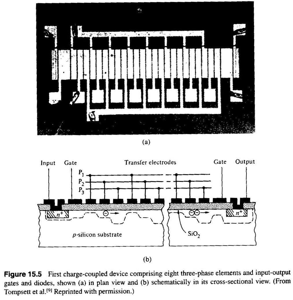
1 Ch 15. Field effect Introduction-The J-FET and MESFET : (a) The device worked on the principle that a voltage applied to the metallic plate modulated the conductance of the underlying semiconductor, which in turn modulated the current flowing between ohmic contacts A and B. This phenomenon, where the conductivity of a semiconductor is modulated by an electric field applied normal to the surface of the semiconductor, has been named the field effect. (b) A key component of present-day microelectronics, the metal-oxide-semiconductor field effect transistor (MOSFET), achieved practical status during the early 1960s. The structure with thermally grown SiO 2 functioning as the gate insulator, a surface-inversion channel, and islands doped opposite to the substrate acting as the source and drain was first reported by Kahng and Atalla in 1960: 1
2 1. General Introduction 1. General Introduction 1) Like bipolar junction transistor, junction field effect transistor JFET is also a threeterminal device but it is a unipolar device, which shall mean that the current is made of either electron or hole carrier. 2) The operation of JFET is controlled by electric field effect. Thus, JFET is a voltagecontrolled current source device, whereas BJT is a current-controlled source device. 3) There are two types of JFET namely n-channel and p-channel. n-channel type means the carrier type in the conducting channel is electron. Likewise, for p-channel type, the carrier type in conducting channel is hole. 4) JFET has three terminals, which are gate G, drain D and source S. The gate is used to control the flow of carrier from source to drain. Source is the terminal that emits carrier and the drain is the terminal that receives carrier. 2
3 JFET: The structures of n-channel and p-channel JFETs are shown (a) n-channel JFET (b) p-channel JFET The structures of n-channel and p-channel 3
4 JFET: The symbols of n-channel and p-channel JFETs (a) n-channel JFET (b) p-channel JFET Symbols of n-channel and p-channel JFET 4
5 2. JEFT 5
6 6
7 7
8 8
9 9
10 10
11 J-FET 11
12 2. Biasing the JFET 3. Biasing the JFET 1) In normal operation, the gate of JFET is always reverse-biased. Thus, an n-channel type, the gate is biased with negative voltage i.e. gate voltage is less than zero volt V G < 0, whilst for p-channel type, the gate is biased with positive voltage i.e. gate voltage is greater than zero voltage V G > 0. 2) The source and drain are biased according to the channel type or carrier type. If it is an n-channel JFET (electron as carrier), the source is biased with negative voltage while the drain is biased with positive voltage. Alternatively, it can be biased such that the drain voltage V D is greater than the source voltage V S. i.e. V D > V S. 3) If it is a p-channel JFET (hole as carrier), the source is biased with positive voltage while the drain is biased with negative voltage. Alternatively, it can be biased such that the drain voltage V D is less than the source voltage V S. i.e. V D < V S. 12

13 2. Biasing the JFET : (a) The depletion regions extend primarily into the lightly doped n-region of the device. When stepping V D to small positive voltages, a current, I D, begins to flow into the drain and through the nondepleted n-region sandwiched between the two p + -n junctions, where the nondepleted current-carrying region is referred to as the channel. For small V D, the channel looks and acts like a simple resistor and the resulting variation of I D with V D is linear. (b) When V D is increased above a few tenths of a volt, the device typically enters a new phase of operation. Since the source is grounded, it naturally follows that somewhere in the channel the potential takes on the gradual changes of voltage, with the potential increasing as one progresses from the source to the drain. (c) consequently, the applied drain bias leads indirectly to a reverse biasing of the gate junctions and an increase in the junction depletion widths. Moreover, the top and bottom depletion regions progressively widen in going down the channel from the source to the drain. 13
14 2. Biasing the JFET (d) Still thinking of the channel region as a resistor, but no longer a simple resistor, one would expect the loss of conductive volume to increase the source-to-drain resistance and reduce the ΔI D resulting from a given change in drain voltage. The slope of the I D -V D characteristic decreases at larger drain biases because of the channel-narrowing effect. (e) Continuing to increase the drain voltage obviously causes the channel to narrow more and more, especially near the drain, until eventually the top and bottom depletion regions touch in the near vicinity of the drain. The complete depletion of the chnnel is an important special condition and is referred to as pinch-off. When the channel pinches off inside the device, the solpe of the I D -V D characteristic becomes approximately zero, and the drain bias at the pinch-off point is given the special designation V Dsat. 14
15 15
16 16
17 4. I-V characteristics B C A 17
18 18
FET(Field Effect Transistor)
") Field Effect Transistor: Construction and Characteristic of JFETs. Transfer Characteristic. CS,CD,CG amplifier and analysis of CS amplifier MOSFET (Depletion and Enhancement) Type, Transfer Characteristic,
Field Effect Transistor: Construction and Characteristic of JFETs. Transfer Characteristic. CS,CD,CG amplifier and analysis of CS amplifier MOSFET (Depletion and Enhancement) Type, Transfer Characteristic,
FIELD EFFECT TRANSISTORS MADE BY : GROUP (13)/PM
/PM") FIELD EFFECT TRANSISTORS MADE BY : GROUP (13)/PM THE FIELD EFFECT TRANSISTOR (FET) In 1945, Shockley had an idea for making a solid state device out of semiconductors. He reasoned that a strong electrical
FIELD EFFECT TRANSISTORS MADE BY : GROUP (13)/PM THE FIELD EFFECT TRANSISTOR (FET) In 1945, Shockley had an idea for making a solid state device out of semiconductors. He reasoned that a strong electrical
6. Field-Effect Transistor
 6. Outline: Introduction to three types of FET: JFET MOSFET & CMOS MESFET Constructions, Characteristics & Transfer curves of: JFET & MOSFET Introduction The field-effect transistor (FET) is a threeterminal
EDC UNIT IV- Transistor and FET Characteristics EDC Lesson 9- ", Raj Kamal, 1
 EDC UNIT IV- Transistor and FET Characteristics Lesson-9: JFET and Construction of JFET 2008 EDC Lesson 9- ", Raj Kamal, 1 1. Transistor 2008 EDC Lesson 9- ", Raj Kamal, 2 Transistor Definition The transferred-resistance
KOM2751 Analog Electronics :: Dr. Muharrem Mercimek :: YTU - Control and Automation Dept. 1 6 FIELD-EFFECT TRANSISTORS
 KOM2751 Analog Electronics :: Dr. Muharrem Mercimek :: YTU - Control and Automation Dept. 1 6 FIELD-EFFECT TRANSISTORS Most of the content is from the textbook: Electronic devices and circuit theory, Robert
Three Terminal Devices
 Three Terminal Devices - field effect transistor (FET) - bipolar junction transistor (BJT) - foundation on which modern electronics is built - active devices - devices described completely by considering
THE JFET. Script. Discuss the JFET and how it differs from the BJT. Describe the basic structure of n-channel and p -channel JFETs
 Course: B.Sc. Applied Physical Science (Computer Science) Year & Sem.: Ist Year, Sem - IInd Subject: Electronics Paper No.: V Paper Title: Analog Circuits Lecture No.: 12 Lecture Title: Analog Circuits
FIELD EFFECT TRANSISTORS
 FIELD EFFECT TRANSISTORS Module 5 Introduction Symbol Features: 1. Voltage is applied across gate and source terminals. This voltage controls the drain current. Hence FET is a voltage controlled device.
Field-Effect Transistor
 Philadelphia University Faculty of Engineering Communication and Electronics Engineering Field-Effect Transistor Introduction FETs (Field-Effect Transistors) are much like BJTs (Bipolar Junction Transistors).
CHAPTER 8 FIELD EFFECT TRANSISTOR (FETs)
") CHAPTER 8 FIELD EFFECT TRANSISTOR (FETs) INTRODUCTION - FETs are voltage controlled devices as opposed to BJT which are current controlled. - There are two types of FETs. o Junction FET (JFET) o Metal
CHAPTER 8 FIELD EFFECT TRANSISTOR (FETs) INTRODUCTION - FETs are voltage controlled devices as opposed to BJT which are current controlled. - There are two types of FETs. o Junction FET (JFET) o Metal
FET. FET (field-effect transistor) JFET. Prepared by Engr. JP Timola Reference: Electronic Devices by Floyd
 JFET. Prepared by Engr. JP Timola Reference: Electronic Devices by Floyd") FET Prepared by Engr. JP Timola Reference: Electronic Devices by Floyd FET (field-effect transistor) unipolar devices - unlike BJTs that use both electron and hole current, they operate only with one type
FET Prepared by Engr. JP Timola Reference: Electronic Devices by Floyd FET (field-effect transistor) unipolar devices - unlike BJTs that use both electron and hole current, they operate only with one type
I E I C since I B is very small
 Figure 2: Symbols and nomenclature of a (a) npn and (b) pnp transistor. The BJT consists of three regions, emitter, base, and collector. The emitter and collector are usually of one type of doping, while
EIE209 Basic Electronics. Transistor Devices. Contents BJT and FET Characteristics Operations. Prof. C.K. Tse: T ransistor devices
 EIE209 Basic Electronics Transistor Devices Contents BJT and FET Characteristics Operations 1 What is a transistor? Three-terminal device whose voltage-current relationship is controlled by a third voltage
Chapter 5: Field Effect Transistors
 Chapter 5: Field Effect Transistors Slide 1 FET FET s (Field Effect Transistors) are much like BJT s (Bipolar Junction Transistors). Similarities: Amplifiers Switching devices Impedance matching circuits
UNIT-VI FIELD EFFECT TRANSISTOR. 1. Explain about the Field Effect Transistor and also mention types of FET s.
 UNIT-I FIELD EFFECT TRANSISTOR 1. Explain about the Field Effect Transistor and also mention types of FET s. The Field Effect Transistor, or simply FET however, uses the voltage that is applied to their
Field Effect Transistors
 Chapter 5: Field Effect Transistors Slide 1 FET FET s (Field Effect Transistors) are much like BJT s (Bipolar Junction Transistors). Similarities: Amplifiers Switching devices Impedance matching circuits
Lecture - 18 Transistors
 Electronic Materials, Devices and Fabrication Dr. S. Prarasuraman Department of Metallurgical and Materials Engineering Indian Institute of Technology, Madras Lecture - 18 Transistors Last couple of classes
FIELD EFFECT TRANSISTOR (FET) 1. JUNCTION FIELD EFFECT TRANSISTOR (JFET)
 1. JUNCTION FIELD EFFECT TRANSISTOR (JFET)") FIELD EFFECT TRANSISTOR (FET) The field-effect transistor (FET) is a three-terminal device used for a variety of applications that match, to a large extent, those of the BJT transistor. Although there
FIELD EFFECT TRANSISTOR (FET) The field-effect transistor (FET) is a three-terminal device used for a variety of applications that match, to a large extent, those of the BJT transistor. Although there
Chapter 8. Field Effect Transistor
 Chapter 8. Field Effect Transistor Field Effect Transistor: The field effect transistor is a semiconductor device, which depends for its operation on the control of current by an electric field. There
Lecture 14. Field Effect Transistor (FET) Sunday 26/11/2017 FET 1-1
 Sunday 26/11/2017 FET 1-1") Lecture 14 Field Effect Transistor (FET) Sunday 26/11/2017 FET 1-1 Outline Introduction to FET transistors Types of FET Transistors Junction Field Effect Transistor (JFET) Characteristics Construction
Lecture 14 Field Effect Transistor (FET) Sunday 26/11/2017 FET 1-1 Outline Introduction to FET transistors Types of FET Transistors Junction Field Effect Transistor (JFET) Characteristics Construction
Lecture 17. Field Effect Transistor (FET) FET 1-1
 FET 1-1") Lecture 17 Field Effect Transistor (FET) FET 1-1 Outline ntroduction to FET transistors Comparison with BJT transistors FET Types Construction and Operation of FET Characteristics Of FET Examples FET 1-2
Lecture 17 Field Effect Transistor (FET) FET 1-1 Outline ntroduction to FET transistors Comparison with BJT transistors FET Types Construction and Operation of FET Characteristics Of FET Examples FET 1-2
ITT Technical Institute. ET215 Devices 1. Unit 7 Chapter 4, Sections
 ITT Technical Institute ET215 Devices 1 Unit 7 Chapter 4, Sections 4.1 4.3 Chapter 4 Section 4.1 Structure of Field-Effect Transistors Recall that the BJT is a current-controlling device; the field-effect
UNIT 3 Transistors JFET
 UNIT 3 Transistors JFET Mosfet Definition of BJT A bipolar junction transistor is a three terminal semiconductor device consisting of two p-n junctions which is able to amplify or magnify a signal. It
TRANSISTOR TRANSISTOR
 It is made up of semiconductor material such as Si and Ge. Usually, it comprises of three terminals namely, base, emitter and collector for providing connection to the external circuit. Today, some transistors
Chapter 6: Field-Effect Transistors
 Chapter 6: Field-Effect Transistors FETs vs. BJTs Similarities: Amplifiers Switching devices Impedance matching circuits Differences: FETs are voltage controlled devices. BJTs are current controlled devices.
INTRODUCTION: Basic operating principle of a MOSFET:
 INTRODUCTION: Along with the Junction Field Effect Transistor (JFET), there is another type of Field Effect Transistor available whose Gate input is electrically insulated from the main current carrying
Chapter 6: Field-Effect Transistors
 Chapter 6: Field-Effect Transistors Islamic University of Gaza Dr. Talal Skaik MOSFETs MOSFETs have characteristics similar to JFETs and additional characteristics that make then very useful. There are
Field-Effect Transistor
 Module: Electronics Module Number: 610/6501- Philadelphia University Faculty of Engineering Communication and Electronics Engineering Field-Effect Transistor ntroduction FETs (Field-Effect Transistors)
UNIT 3: FIELD EFFECT TRANSISTORS
 FIELD EFFECT TRANSISTOR: UNIT 3: FIELD EFFECT TRANSISTORS The field effect transistor is a semiconductor device, which depends for its operation on the control of current by an electric field. There are
Field - Effect Transistor
 Page 1 of 6 Field - Effect Transistor Aim :- To draw and study the out put and transfer characteristics of the given FET and to determine its parameters. Apparatus :- FET, two variable power supplies,
Digital Electronics. By: FARHAD FARADJI, Ph.D. Assistant Professor, Electrical and Computer Engineering, K. N. Toosi University of Technology
 K. N. Toosi University of Technology Chapter 7. Field-Effect Transistors By: FARHAD FARADJI, Ph.D. Assistant Professor, Electrical and Computer Engineering, K. N. Toosi University of Technology http://wp.kntu.ac.ir/faradji/digitalelectronics.htm
2.9 Junction field-effect transistors
 2.9 Junction field-effect transistors The field effect transistor was proposed by Julius Lilienfeld in U patents in 1926 and 1933 (1,900,018). Moreover, hockley, Brattain, and Bardeen were investigating
EE 5611 Introduction to Microelectronic Technologies Fall Thursday, September 04, 2014 Lecture 02
 EE 5611 Introduction to Microelectronic Technologies Fall 2014 Thursday, September 04, 2014 Lecture 02 1 Lecture Outline Review on semiconductor materials Review on microelectronic devices Example of microelectronic
Lecture 15. Field Effect Transistor (FET) Wednesday 29/11/2017 MOSFET 1-1
 Wednesday 29/11/2017 MOSFET 1-1") Lecture 15 Field Effect Transistor (FET) Wednesday 29/11/2017 MOSFET 1-1 Outline MOSFET transistors Introduction to MOSFET MOSFET Types epletion-type MOSFET Characteristics Comparison between JFET and
Lecture 15 Field Effect Transistor (FET) Wednesday 29/11/2017 MOSFET 1-1 Outline MOSFET transistors Introduction to MOSFET MOSFET Types epletion-type MOSFET Characteristics Comparison between JFET and
FET. Field Effect Transistors ELEKTRONIKA KONTROL. Eka Maulana, ST, MT, M.Eng. Universitas Brawijaya. p + S n n-channel. Gate. Basic structure.
 FET Field Effect Transistors ELEKTRONIKA KONTROL Basic structure Gate G Source S n n-channel Cross section p + p + p + G Depletion region Drain D Eka Maulana, ST, MT, M.Eng. Universitas Brawijaya S Channel
Solid State Device Fundamentals
 Solid State Device Fundamentals 4.4. Field Effect Transistor (MOSFET) ENS 463 Lecture Course by Alexander M. Zaitsev alexander.zaitsev@csi.cuny.edu Tel: 718 982 2812 4N101b 1 Field-effect transistor (FET)
(Refer Slide Time: 02:05)
") Electronics for Analog Signal Processing - I Prof. K. Radhakrishna Rao Department of Electrical Engineering Indian Institute of Technology Madras Lecture 27 Construction of a MOSFET (Refer Slide Time:
Electronics for Analog Signal Processing - I Prof. K. Radhakrishna Rao Department of Electrical Engineering Indian Institute of Technology Madras Lecture 27 Construction of a MOSFET (Refer Slide Time:
COLLECTOR DRAIN BASE GATE EMITTER. Applying a voltage to the Gate connection allows current to flow between the Drain and Source connections.
 MOSFETS Although the base current in a transistor is usually small (< 0.1 ma), some input devices (e.g. a crystal microphone) may be limited in their output. In order to overcome this, a Field Effect Transistor
Electronic Circuits. Junction Field-effect Transistors. Dr. Manar Mohaisen Office: F208 Department of EECE
 Electronic Circuits Junction Field-effect Transistors Dr. Manar Mohaisen Office: F208 Email: manar.subhi@kut.ac.kr Department of EECE Review of the Precedent Lecture Explain the Operation Class A Power
Basic Electronics Prof. Dr. Chitralekha Mahanta Department of Electronics and Communication Engineering Indian Institute of Technology, Guwahati
 Basic Electronics Prof. Dr. Chitralekha Mahanta Department of Electronics and Communication Engineering Indian Institute of Technology, Guwahati Module: 3 Field Effect Transistors Lecture-7 High Frequency
Field Effect Transistor (FET) FET 1-1
 FET 1-1") Field Effect Transistor (FET) FET 1-1 Outline MOSFET transistors ntroduction to MOSFET MOSFET Types epletion-type MOSFET Characteristics Biasing Circuits and Examples Comparison between JFET and epletion-type
Field Effect Transistor (FET) FET 1-1 Outline MOSFET transistors ntroduction to MOSFET MOSFET Types epletion-type MOSFET Characteristics Biasing Circuits and Examples Comparison between JFET and epletion-type
IENGINEERS-CONSULTANTS QUESTION BANK SERIES ELECTRONICS ENGINEERING 1 YEAR UPTU ELECTRONICS ENGINEERING EC 101 UNIT 3 (JFET AND MOSFET)
") ELECTRONICS ENGINEERING EC 101 UNIT 3 (JFET AND MOSFET) LONG QUESTIONS (10 MARKS) 1. Draw the construction diagram and explain the working of P-Channel JFET. Also draw the characteristics curve and transfer
ELECTRONICS ENGINEERING EC 101 UNIT 3 (JFET AND MOSFET) LONG QUESTIONS (10 MARKS) 1. Draw the construction diagram and explain the working of P-Channel JFET. Also draw the characteristics curve and transfer
ITT Technical Institute. ET215 Devices 1. Unit 8 Chapter 4, Sections
 ITT Technical Institute ET215 Devices 1 Unit 8 Chapter 4, Sections 4.4 4.5 Chapter 4 Section 4.4 MOSFET Characteristics A Metal-Oxide semiconductor field-effect transistor is the other major category of
EE70 - Intro. Electronics
 EE70 - Intro. Electronics Course website: ~/classes/ee70/fall05 Today s class agenda (November 28, 2005) review Serial/parallel resonant circuits Diode Field Effect Transistor (FET) f 0 = Qs = Qs = 1 2π
INTRODUCTION TO MOS TECHNOLOGY
 INTRODUCTION TO MOS TECHNOLOGY 1. The MOS transistor The most basic element in the design of a large scale integrated circuit is the transistor. For the processes we will discuss, the type of transistor
Lecture 13. Metal Oxide Semiconductor Field Effect Transistor (MOSFET) MOSFET 1-1
 MOSFET 1-1") Lecture 13 Metal Oxide Semiconductor Field Effect Transistor (MOSFET) MOSFET 1-1 Outline Continue MOSFET Qualitative Operation epletion-type MOSFET Characteristics Biasing Circuits and Examples Enhancement-type
Lecture 13 Metal Oxide Semiconductor Field Effect Transistor (MOSFET) MOSFET 1-1 Outline Continue MOSFET Qualitative Operation epletion-type MOSFET Characteristics Biasing Circuits and Examples Enhancement-type
Lecture 3: Transistors
 Lecture 3: Transistors Now that we know about diodes, let s put two of them together, as follows: collector base emitter n p n moderately doped lightly doped, and very thin heavily doped At first glance,
Analog Electronics. Electronic Devices, 9th edition Thomas L. Floyd Pearson Education. Upper Saddle River, NJ, All rights reserved.
 Analog Electronics BJT Structure The BJT has three regions called the emitter, base, and collector. Between the regions are junctions as indicated. The base is a thin lightly doped region compared to the
Summary. Electronics II Lecture 5(b): Metal-Oxide Si FET MOSFET. A/Lectr. Khalid Shakir Dept. Of Electrical Engineering
: Metal-Oxide Si FET MOSFET. A/Lectr. Khalid Shakir Dept. Of Electrical Engineering") Summary Electronics II Lecture 5(b): Metal-Oxide Si FET MOSFET A/Lectr. Khalid Shakir Dept. Of Electrical Engineering College of Engineering Maysan University Page 1-21 Summary The MOSFET The metal oxide
Summary Electronics II Lecture 5(b): Metal-Oxide Si FET MOSFET A/Lectr. Khalid Shakir Dept. Of Electrical Engineering College of Engineering Maysan University Page 1-21 Summary The MOSFET The metal oxide
value of W max for the device. The at band voltage is -0.9 V. Problem 5: An Al-gate n-channel MOS capacitor has a doping of N a = cm ;3. The oxi
 Prof. Jasprit Singh Fall 2001 EECS 320 Homework 10 This homework is due on December 6 Problem 1: An n-type In 0:53 Ga 0:47 As epitaxial layer doped at 10 16 cm ;3 is to be used as a channel in a FET. A
THE METAL-SEMICONDUCTOR CONTACT
 THE METAL-SEMICONDUCTOR CONTACT PROBLEM 1 To calculate the theoretical barrier height, built-in potential barrier, and maximum electric field in a metal-semiconductor diode for zero applied bias. Consider
Electronics I. Last Time
 (Rev. 1.0) Electronics I Lecture 28 Introduction to Field Effect Transistors (FET s) Muhammad Tilal Department of Electrical Engineering CIIT Attock Campus The logo and is the property of CIIT, Pakistan
Field-Effect Transistor (FET) is one of the two major transistors; FET derives its name from its working mechanism;
 is one of the two major transistors; FET derives its name from its working mechanism;") Chapter 3 Field-Effect Transistors (FETs) 3.1 Introduction Field-Effect Transistor (FET) is one of the two major transistors; FET derives its name from its working mechanism; The concept has been known
Chapter 3 Field-Effect Transistors (FETs) 3.1 Introduction Field-Effect Transistor (FET) is one of the two major transistors; FET derives its name from its working mechanism; The concept has been known
MODULE-2: Field Effect Transistors (FET)
") FORMAT-1B Definition: MODULE-2: Field Effect Transistors (FET) FET is a three terminal electronic device used for variety of applications that match with BJT. In FET, an electric field is established by
FORMAT-1B Definition: MODULE-2: Field Effect Transistors (FET) FET is a three terminal electronic device used for variety of applications that match with BJT. In FET, an electric field is established by
ECE 340 Lecture 37 : Metal- Insulator-Semiconductor FET Class Outline:
 ECE 340 Lecture 37 : Metal- Insulator-Semiconductor FET Class Outline: Metal-Semiconductor Junctions MOSFET Basic Operation MOS Capacitor Things you should know when you leave Key Questions What is the
4.1 Device Structure and Physical Operation
 10/12/2004 4_1 Device Structure and Physical Operation blank.doc 1/2 4.1 Device Structure and Physical Operation Reading Assignment: pp. 235-248 Chapter 4 covers Field Effect Transistors ( ) Specifically,
Lecture (09) The JFET (2)
 The JFET (2)") Lecture (09) The JFET (2) By: r. Ahmed Elhafee ١ V Controls I connect a bias voltage, V V is set to increasingly more negative values by adjusting V, a family of drain characteristic curves is produced.
Lecture (09) The JFET (2) By: r. Ahmed Elhafee ١ V Controls I connect a bias voltage, V V is set to increasingly more negative values by adjusting V, a family of drain characteristic curves is produced.
Unit III FET and its Applications. 2 Marks Questions and Answers
 Unit III FET and its Applications 2 Marks Questions and Answers 1. Why do you call FET as field effect transistor? The name field effect is derived from the fact that the current is controlled by an electric
Radio Frequency Electronics
 Radio Frequency Electronics Active Components II Harry Nyquist Born in 1889 in Sweden Received B.S. and M.S. from U. North Dakota Received Ph.D. from Yale Worked and Bell Laboratories for all of his career
MEASUREMENT AND INSTRUMENTATION STUDY NOTES UNIT-I
 MEASUREMENT AND INSTRUMENTATION STUDY NOTES The MOSFET The MOSFET Metal Oxide FET UNIT-I As well as the Junction Field Effect Transistor (JFET), there is another type of Field Effect Transistor available
Conduction Characteristics of MOS Transistors (for fixed Vds)! Topic 2. Basic MOS theory & SPICE simulation. MOS Transistor
! Topic 2. Basic MOS theory & SPICE simulation. MOS Transistor") Conduction Characteristics of MOS Transistors (for fixed Vds)! Topic 2 Basic MOS theory & SPICE simulation Peter Cheung Department of Electrical & Electronic Engineering Imperial College London (Weste&Harris,
Conduction Characteristics of MOS Transistors (for fixed Vds)! Topic 2 Basic MOS theory & SPICE simulation Peter Cheung Department of Electrical & Electronic Engineering Imperial College London (Weste&Harris,
Topic 2. Basic MOS theory & SPICE simulation
 Topic 2 Basic MOS theory & SPICE simulation Peter Cheung Department of Electrical & Electronic Engineering Imperial College London (Weste&Harris, Ch 2 & 5.1-5.3 Rabaey, Ch 3) URL: www.ee.ic.ac.uk/pcheung/
Conduction Characteristics of MOS Transistors (for fixed Vds) Topic 2. Basic MOS theory & SPICE simulation. MOS Transistor
 Topic 2. Basic MOS theory & SPICE simulation. MOS Transistor") Conduction Characteristics of MOS Transistors (for fixed Vds) Topic 2 Basic MOS theory & SPICE simulation Peter Cheung Department of Electrical & Electronic Engineering Imperial College London (Weste&Harris,
Conduction Characteristics of MOS Transistors (for fixed Vds) Topic 2 Basic MOS theory & SPICE simulation Peter Cheung Department of Electrical & Electronic Engineering Imperial College London (Weste&Harris,
Analog Electronic Circuits Prof. S. C. Dutta Roy Department of Electrical Engineering Indian Institute of Technology Delhi Lecture No 03
 Analog Electronic Circuits Prof. S. C. Dutta Roy Department of Electrical Engineering Indian Institute of Technology Delhi Lecture No 03 Before we take FETs let us recall and example which we had taken
Intro to Electricity. Introduction to Transistors. Example Circuit Diagrams. Water Analogy
 Introduction to Transistors Transistors form the basic building blocks of all computer hardware. Invented by William Shockley, John Bardeen and Walter Brattain in 1947, replacing previous vaccuumtube technology
Depletion-mode operation ( 공핍형 ): Using an input gate voltage to effectively decrease the channel size of an FET
: Using an input gate voltage to effectively decrease the channel size of an FET") Ch. 13 MOSFET Metal-Oxide-Semiconductor Field-Effect Transistor : I D D-mode E-mode V g The gate oxide is made of dielectric SiO 2 with e = 3.9 Depletion-mode operation ( 공핍형 ): Using an input gate voltage
Ch. 13 MOSFET Metal-Oxide-Semiconductor Field-Effect Transistor : I D D-mode E-mode V g The gate oxide is made of dielectric SiO 2 with e = 3.9 Depletion-mode operation ( 공핍형 ): Using an input gate voltage
Difference between BJTs and FETs. Junction Field Effect Transistors (JFET)
") Difference between BJTs and FETs Transistors can be categorized according to their structure, and two of the more commonly known transistor structures, are the BJT and FET. The comparison between BJTs
Difference between BJTs and FETs Transistors can be categorized according to their structure, and two of the more commonly known transistor structures, are the BJT and FET. The comparison between BJTs
Electronic Circuits II - Revision
 Electronic Circuits II - Revision -1 / 16 - T & F # 1 A bypass capacitor in a CE amplifier decreases the voltage gain. 2 If RC in a CE amplifier is increased, the voltage gain is reduced. 3 4 5 The load
Prof. Paolo Colantonio a.a
 Prof. Paolo Colantonio a.a. 20 2 Field effect transistors (FETs) are probably the simplest form of transistor, widely used in both analogue and digital applications They are characterised by a very high
Lecture (03) The JFET
 The JFET") Lecture (03) The JFET By: Dr. Ahmed ElShafee ١ JFET Basic Structure Figure shows the basic structure of an n channel JFET (junction field effect transistor). Wire leads are connected to each end of the
Lecture (03) The JFET By: Dr. Ahmed ElShafee ١ JFET Basic Structure Figure shows the basic structure of an n channel JFET (junction field effect transistor). Wire leads are connected to each end of the
Field Effect Transistors (npn)
") Field Effect Transistors (npn) gate drain source FET 3 terminal device channel e - current from source to drain controlled by the electric field generated by the gate base collector emitter BJT 3 terminal
Field Effect Transistors (npn) gate drain source FET 3 terminal device channel e - current from source to drain controlled by the electric field generated by the gate base collector emitter BJT 3 terminal
L MOSFETS, IDENTIFICATION, CURVES. PAGE 1. I. Review of JFET (DRAW symbol for n-channel type, with grounded source)
") L.107.4 MOSFETS, IDENTIFICATION, CURVES. PAGE 1 I. Review of JFET (DRAW symbol for n-channel type, with grounded source) 1. "normally on" device A. current from source to drain when V G = 0 no need to
L.107.4 MOSFETS, IDENTIFICATION, CURVES. PAGE 1 I. Review of JFET (DRAW symbol for n-channel type, with grounded source) 1. "normally on" device A. current from source to drain when V G = 0 no need to
(a) Current-controlled and (b) voltage-controlled amplifiers.
 Current-controlled and (b) voltage-controlled amplifiers.") Fig. 6.1 (a) Current-controlled and (b) voltage-controlled amplifiers. Fig. 6.2 Drs. Ian Munro Ross (front) and G. C. Dacey jointly developed an experimental procedure for measuring the characteristics
Fig. 6.1 (a) Current-controlled and (b) voltage-controlled amplifiers. Fig. 6.2 Drs. Ian Munro Ross (front) and G. C. Dacey jointly developed an experimental procedure for measuring the characteristics
Field Effect Transistors
 Field Effect Transistors LECTURE NO. - 41 Field Effect Transistors www.mycsvtunotes.in JFET MOSFET CMOS Field Effect transistors - FETs First, why are we using still another transistor? BJTs had a small
Integrated diodes. The forward voltage drop only slightly depends on the forward current. ELEKTRONIKOS ĮTAISAI
 1 Integrated diodes pn junctions of transistor structures can be used as integrated diodes. The choice of the junction is limited by the considerations of switching speed and breakdown voltage. The forward
EDC UNIT IV- Transistor and FET JFET Characteristics EDC Lesson 4- ", Raj Kamal, 1
 EDC UNIT IV- Transistor and FET Characteristics Lesson-10: JFET Characteristics Qualitative Discussion 2008 EDC Lesson 4- ", Raj Kamal, 1 n-junction FET and p-jfet Symbols D D + D G + V DS V DS V GS S
Basic Electronics. Introductory Lecture Course for. Technology and Instrumentation in Particle Physics Chicago, Illinois June 9-14, 2011
 Basic Electronics Introductory Lecture Course for Technology and Instrumentation in Particle Physics 2011 Chicago, Illinois June 9-14, 2011 Presented By Gary Drake Argonne National Laboratory Session 3
Semiconductor Physics and Devices
 Metal-Semiconductor and Semiconductor Heterojunctions The Metal-Oxide-Semiconductor Field-Effect Transistor (MOSFET) is one of two major types of transistors. The MOSFET is used in digital circuit, because
EE301 Electronics I , Fall
 EE301 Electronics I 2018-2019, Fall 1. Introduction to Microelectronics (1 Week/3 Hrs.) Introduction, Historical Background, Basic Consepts 2. Rewiev of Semiconductors (1 Week/3 Hrs.) Semiconductor materials
Q1. Explain the construction and principle of operation of N-Channel and P-Channel Junction Field Effect Transistor (JFET).
.") Q. Explain the construction and principle of operation of N-Channel and P-Channel Junction Field Effect Transistor (JFET). Answer: N-Channel Junction Field Effect Transistor (JFET) Construction: Drain(D)
Q. Explain the construction and principle of operation of N-Channel and P-Channel Junction Field Effect Transistor (JFET). Answer: N-Channel Junction Field Effect Transistor (JFET) Construction: Drain(D)
Lecture 20. MOSFET (cont d) MOSFET 1-1
 MOSFET 1-1") Lecture 0 MOSFET (cont d) MOSFET 1-1 Outline Continue Enhancement-type MOSFET (E- MOSFET) Characteristics C Biasing Circuits and Examples MOSFET 1- Test Yourself Complete the following statements with
Lecture 0 MOSFET (cont d) MOSFET 1-1 Outline Continue Enhancement-type MOSFET (E- MOSFET) Characteristics C Biasing Circuits and Examples MOSFET 1- Test Yourself Complete the following statements with
5.1 Introduction. transistor. Like the bipolar junction transistors (BJTs) we studied in Chapter 4,
 we studied in Chapter 4,") 5.1 Introduction In this chapter we introduce the second major type of transistor: the field-effect transistor. Like the bipolar junction transistors (BJTs) we studied in Chapter 4, field-effect transistors
5.1 Introduction In this chapter we introduce the second major type of transistor: the field-effect transistor. Like the bipolar junction transistors (BJTs) we studied in Chapter 4, field-effect transistors
ELECTRONIC DEVICES AND CIRCUITS
 ELECTRONIC DEVICES AND CIRCUITS 1. At room temperature the current in an intrinsic semiconductor is due to A. holes B. electrons C. ions D. holes and electrons 2. Work function is the maximum energy required
The Common Source JFET Amplifier
 The Common Source JFET Amplifier Small signal amplifiers can also be made using Field Effect Transistors or FET's for short. These devices have the advantage over bipolar transistors of having an extremely
UNIVERSITY OF CALIFORNIA AT BERKELEY College of Engineering Department of Electrical Engineering and Computer Sciences.
 UNIVERSITY OF CALIFORNIA AT BERKELEY College of Engineering Department of Electrical Engineering and Computer Sciences Discussion #9 EE 05 Spring 2008 Prof. u MOSFETs The standard MOSFET structure is shown
Power MOSFET Zheng Yang (ERF 3017,
 ECE442 Power Semiconductor Devices and Integrated Circuits Power MOSFET Zheng Yang (ERF 3017, email: yangzhen@uic.edu) Evolution of low-voltage (
Power Bipolar Junction Transistors (BJTs)
") ECE442 Power Semiconductor Devices and Integrated Circuits Power Bipolar Junction Transistors (BJTs) Zheng Yang (ERF 3017, email: yangzhen@uic.edu) Power Bipolar Junction Transistor (BJT) Background The
ECE442 Power Semiconductor Devices and Integrated Circuits Power Bipolar Junction Transistors (BJTs) Zheng Yang (ERF 3017, email: yangzhen@uic.edu) Power Bipolar Junction Transistor (BJT) Background The
Lesson 5. Electronics: Semiconductors Doping p-n Junction Diode Half Wave and Full Wave Rectification Introduction to Transistors-
 Lesson 5 Electronics: Semiconductors Doping p-n Junction Diode Half Wave and Full Wave Rectification Introduction to Transistors- Types and Connections Semiconductors Semiconductors If there are many free
UNIT-1 Bipolar Junction Transistors. Text Book:, Microelectronic Circuits 6 ed., by Sedra and Smith, Oxford Press
 UNIT-1 Bipolar Junction Transistors Text Book:, Microelectronic Circuits 6 ed., by Sedra and Smith, Oxford Press Figure 6.1 A simplified structure of the npn transistor. Microelectronic Circuits, Sixth
Reg. No. : Question Paper Code : B.E./B.Tech. DEGREE EXAMINATION, NOVEMBER/DECEMBER Second Semester
 WK 5 Reg. No. : Question Paper Code : 27184 B.E./B.Tech. DEGREE EXAMINATION, NOVEMBER/DECEMBER 2015. Time : Three hours Second Semester Electronics and Communication Engineering EC 6201 ELECTRONIC DEVICES
Bipolar Junction Transistor (BJT) Basics- GATE Problems
 Basics- GATE Problems") Bipolar Junction Transistor (BJT) Basics- GATE Problems One Mark Questions 1. The break down voltage of a transistor with its base open is BV CEO and that with emitter open is BV CBO, then (a) BV CEO =
Bipolar Junction Transistor (BJT) Basics- GATE Problems One Mark Questions 1. The break down voltage of a transistor with its base open is BV CEO and that with emitter open is BV CBO, then (a) BV CEO =
Scheme I Sample. : Second : Basic. Electronics : 70. Marks. Time: 3 Hrs. 2] b) State any. e) State any. Figure Definition.
![Scheme I Sample. : Second : Basic. Electronics : 70. Marks. Time: 3 Hrs. 2] b) State any. e) State any. Figure Definition.](/thumbs/96/128002629.jpg "Scheme I Sample. : Second : Basic. Electronics : 70. Marks. Time: 3 Hrs. 2] b) State any. e) State any. Figure Definition.") Program Name Program Code Semester Course Title Scheme I Sample Question Paper : Diploma in Electronics Program Group : DE/EJ/IE/IS/ET/EN/EX : Second : Basic Electronics : 70 22216 Time: 3 Hrs. Instructions:
Program Name Program Code Semester Course Title Scheme I Sample Question Paper : Diploma in Electronics Program Group : DE/EJ/IE/IS/ET/EN/EX : Second : Basic Electronics : 70 22216 Time: 3 Hrs. Instructions:
UNIT II JFET, MOSFET, SCR & UJT
 UNIT II JFET, MOSFET, SCR & UJT JFET JFET as an Amplifier and its Output Characteristics JFET Applications MOSFET Working Principles, SCR Equivalent Circuit and V-I Characteristics. SCR as a Half wave
Questions on JFET: 1) Which of the following component is a unipolar device?
 Which of the following component is a unipolar device?") Questions on JFET: 1) Which of the following component is a unipolar device? a) BJT b) FET c) DJT d) EFT 2) Current Conduction in FET takes place due e) Majority charge carriers only f) Minority charge
Questions on JFET: 1) Which of the following component is a unipolar device? a) BJT b) FET c) DJT d) EFT 2) Current Conduction in FET takes place due e) Majority charge carriers only f) Minority charge
Lecture (10) MOSFET. By: Dr. Ahmed ElShafee. Dr. Ahmed ElShafee, ACU : Fall 2016, Electronic Circuits II
 MOSFET. By: Dr. Ahmed ElShafee. Dr. Ahmed ElShafee, ACU : Fall 2016, Electronic Circuits II") Lecture (10) MOSFET By: Dr. Ahmed ElShafee ١ Dr. Ahmed ElShafee, ACU : Fall 2017, Electronic Circuits II Introduction The MOSFET (metal oxide semiconductor field effect transistor) is another category
Lecture (10) MOSFET By: Dr. Ahmed ElShafee ١ Dr. Ahmed ElShafee, ACU : Fall 2017, Electronic Circuits II Introduction The MOSFET (metal oxide semiconductor field effect transistor) is another category
Electronic PRINCIPLES
 MALVINO & BATES Electronic PRINCIPLES SEVENTH EDITION Chapter 13 JFETs Topics Covered in Chapter 13 Basic ideas Drain curves Transconductance curve Biasing in the ohmic region Biasing in the active region
F.Y. Diploma : Sem. II [DE/EJ/IE/IS/EE/MU/ET/EN/EX] Basic Electronics
![F.Y. Diploma : Sem. II [DE/EJ/IE/IS/EE/MU/ET/EN/EX] Basic Electronics](/thumbs/95/124107511.jpg "F.Y. Diploma : Sem. II [DE/EJ/IE/IS/EE/MU/ET/EN/EX] Basic Electronics") F.Y. Diploma : Sem. II [DE/EJ/IE/IS/EE/MU/ET/EN/EX] Basic Electronics Time: 3 Hrs.] Prelim Question Paper Solution [Marks : 70 Q.1 Attempt any FIE of the following : [10] Q.1(a) Draw the symbols for (i)
F.Y. Diploma : Sem. II [DE/EJ/IE/IS/EE/MU/ET/EN/EX] Basic Electronics Time: 3 Hrs.] Prelim Question Paper Solution [Marks : 70 Q.1 Attempt any FIE of the following : [10] Q.1(a) Draw the symbols for (i)
MTLE-6120: Advanced Electronic Properties of Materials. Semiconductor transistors for logic and memory. Reading: Kasap
 MTLE-6120: Advanced Electronic Properties of Materials 1 Semiconductor transistors for logic and memory Reading: Kasap 6.6-6.8 Vacuum tube diodes 2 Thermionic emission from cathode Electrons collected
55:041 Electronic Circuits
 55:041 Electronic Circuits Mosfet Review Sections of Chapter 3 &4 A. Kruger Mosfet Review, Page-1 Basic Structure of MOS Capacitor Sect. 3.1 Width 1 10-6 m or less Thickness 50 10-9 m or less ` MOS Metal-Oxide-Semiconductor
Lecture 24: Bipolar Junction Transistors (1) Bipolar Junction Structure, Operating Regions, Biasing
 Bipolar Junction Structure, Operating Regions, Biasing") Lecture 24: Bipolar Junction Transistors (1) Bipolar Junction Structure, Operating Regions, Biasing BJT Structure the BJT is formed by doping three semiconductor regions (emitter, base, and collector)
Lecture 24: Bipolar Junction Transistors (1) Bipolar Junction Structure, Operating Regions, Biasing BJT Structure the BJT is formed by doping three semiconductor regions (emitter, base, and collector)