ET Training. Electronics: JFET Instructor: H.Pham. The JUNCTION FIELF EFFECT TRANSISTOR (JFET) n channel JFET p channel JFET
|
|
|
- Letitia Wood
- 5 years ago
- Views:
Transcription
 n channel JFET p channel JFET")
1 The JUNCTION FIELF EFFECT TRANSISTOR (JFET) n channel JFET p channel JFET 1
2 The BIASED JFET VDD provides a drain-to-source voltage and supplies current from drain to source VGG sets the reverse-biased voltage between gate and source JFET is always operated with the gate-source pn junction reverse-biased. the gate current IG=0 Input resistance Rin = VGG / IG = infinitive ohm Typical JFET has Rin is hundred of mega-ohm JFET is in application where a high input impedance is required one of the most importance of JFET is the source follower 2

3 JFET schematic symbols 3
4 DRAIN CURVES The maximum drain current out of JFET occurs when the GATE- SOURCE voltage is zero The drain current is almost constant in the region between VP and VDS (max) If the drain voltage is too large, the JFET breaks down JFET acts like current source when it is operating along the almost horizontal part of the drain curve. ( between minimum of VP and maximum of VDS (max) ) The minimum voltage of VP is called PINCHOFF voltage The maximum voltage VDS (max) is called breakdown voltage Between PINCHOFF and breakdown the JFET acts like current source with the value of IDSS. IDSS stands for the current from drain to source with shorted gate [VGS=0] The OHMIC region The almost vertical part of the drain curve is called OHMIC region, that equivalent to the saturation region of bipolar transistor 4

5 When operated in the OHMIC region, the JFET acts as small resistor with the value is RDS = VP / IDSS DRAIN CURVES VDS(max) 5
6 VGS controls ID 6
7 Cutoff Voltage The value of VGS that makes ID approximately zero is the cutoff voltage, VGS(off). The JFET must be operated between VGS=0 V and VGS(off) Comparison of Pinch-off and cutoff Vp is the value of VDS at which the drain current becomes constant and is always measured at VGS=0 VGS and VP are always equal in magnitude but opposite in sign. Data sheet usually will give either VGS(off) or VP but not both 7
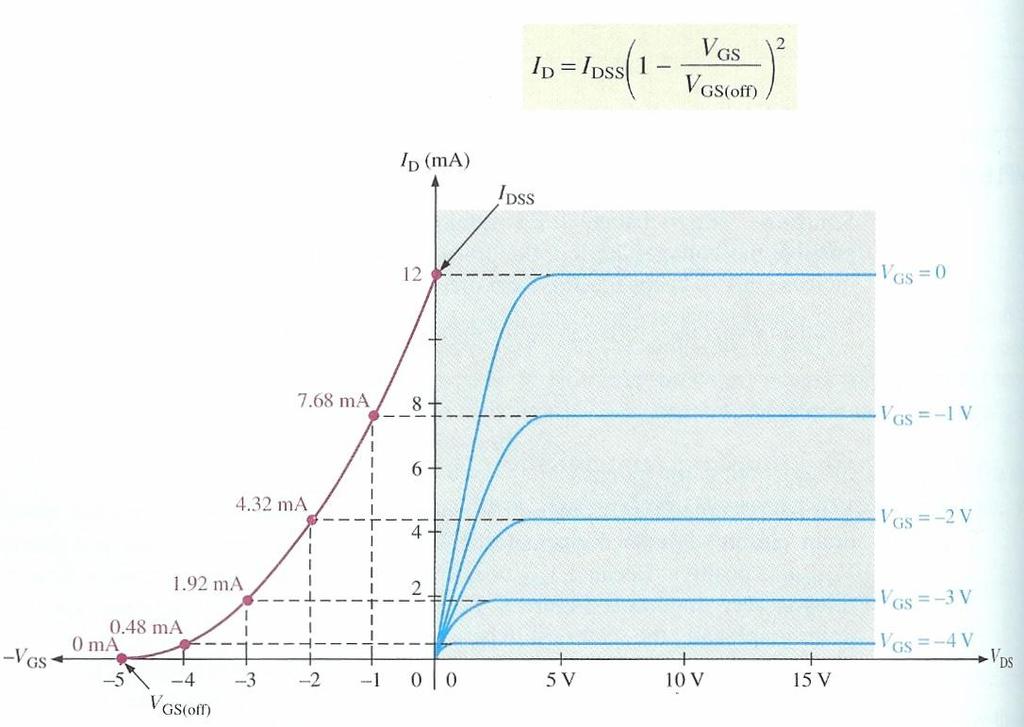
8 JFET TRANSFER CHARACTERISTIC Remember ID=0 when VGS=VGS(off) and ID=IDSS When VGS=0 8
9 9
10 Example#3: The data sheet of JFET 2N5459 indicates that typically IDSS=9 ma and VGS(off)=-8V(maximum). Determine the drain current for VGS=0V, -1V, and -4V. Solution: JFET FORWARD TRANSCONDUCTANCE The forward transfer conductance gm is the change in drain current ( ID) for a given change in gate-to-source voltage ( VGS) with the drain-tosource voltage constant. It is expressed as a ratio and has the unit of siemens (S) gm = ( ID) / VGS 10
11 Data sheet normally gives the value of g m measured at VGS=0 (g m0 ) Given gm0 then calculate gm at any point on the transfer characteristic curve, using the following formula: g m = g m0 ( 1- VGS/ VGS(off) ) If value of gm0 is not available, then calculate gm0 as following: g m0 = 2IDSS/ VGS(off) 11
12 INPUT RESISTANCE AND CAPACITANCE: R IN = V GS / I GSS Example#5: A certain JFET has an IGSS of 2 na for VGS=-20V. Determine the input resistance Solution: R IN = V GS / I GSS = MegaOhm DRAIN-TO-SOURCE RESISTANCE r d = V DS / I D JFET BIASING SELF-BIAS For p-channel: VGS = +I D x R S VD = VDD I D R D VDS = VD VS = VDD ID( R D + R S ) 12
13 Example#6:For the circuit shown, find VDS and VGS, given that ID=5mA 13
14 Voltage-Divider Bias V S = I D x R S or I D = V S / R S V GS = V G V S V S = V G V GS I D = V S / R S = ( V G V GS )/R S Example#8: Determine ID and VGS for the JFET With voltage divider shown Given that VD=7V. Solution: 14
15 Graphical Analysis of a JFET with voltage divider bias For ID=0 VS = ID X RS= 0V VGS=VG-VS=VG For VGS=0 ID= (VG- VGS)/RS) = VG/RS 15
16 16
17 17
18 THE METAL OXIDE SEMICONDUCTOR FET ( MOSFET) The D-MOSFET can be operated of two modes: 1. The depletion mode 2. the enhancement mode Sometimes called Depletion enhancement MOSFET Either positive or negative Gate voltage can be applied Depletion mode: when negative gate-to-source voltage is applied. enhancement mode: when positive gate-to-source voltage is applied. Generally operate in the depletion mode 18

19 Enhancement MOSFET (E-MOSFET) Operates only in the enhancement mode N-channel required positive gate-to-source voltage P-channel required negative gate-to-source voltage Equation transfer characteristic curve differs from that of JFET and D-MOSFET 19
20 20
21 Example: For a certain D-MOSFET, IDSS = 10 ma and VGS(off) = -8 V. 1. Is this an n-channel or p-channel? 2. Calculate ID at VGS=-3 V 3. Calculate ID at VGS=+3 V Related Exercise: For a certain D-MOSFET, IDSS=18 ma and VGS(OFF)=+10 V 1. Is this an n-channel or p-channel? 2. Calculate ID at VGS=+4 V 3. Calculate ID at VGS=-4 V 21
22 22
23 Enhancement MOSFET (E-MOSFET) continue The equation for the E-MOSFET transfer characteristic is: I D = K ( V GS V GS(th) ) 2 the constant K depends on the particular MOSFET Can be determined from data sheet by taking the specified value of ID, called ID(ON) at the given value of VGS Example: The data sheet of a 2N7008 E-MOSFET gives ID(ON)=500 miiliamp at VGS=10 V and Vth=1 V. Determine the drain current for VGS=5 V. Solution: 23
24 Related Exercise: The data sheet of a 2N7008 E-MOSFET gives ID(ON)=100 miiliamp at VGS=8 V and VGS(th)=4 V. Determine the drain current for VGS=6 V. HANDLING Precautions: All MOS devices are subject to damage from electrostatic discharge (ESD) MOS devices should be shipped and stored in conductive foam All instruments and metal benches used in assembly or test should be connected to earth GND. The assembler s or handler s wrist should be connected to earth GND with the length of wire and a high value series resistor. Never remove an MOS device from the circuit while power is ON Do not apply signals while the DC power is OFF 24
25 MOSFET BIASING 1. D-MOSFET Biasing The circuit MOSFET with zero bias shown. VGS=0 and ID=IDSS VDS = VDD IDSS x RD The purpose of RG in the second circuit is to accommodate an ac signal input by isolating it from GND Since there is no dc gate current, RG does not affect The zero gate-to-source bias 25
26 Example: Determine the drain-to-source voltage in the circuit shown. The MOSFET data sheet gives VGS(off)=-8 V and IDSS=12 millia Solution: VDS=10.6 V 26
27 Example: Determine VGS and VDS in the circuit shown. The data sheet for this particular MSFET minimum value of ID(on)=500 millia at VGS=10V and VGS(th) = 1 V. Solution: VGS=(R2/(R1+R2) x VDD = 3.13V Find K: K=ID(on) / (VGS-VGS(th)) 2 = 6.17 millia/v 2 Calculate ID: ID=K(VGS-VGS(th)) 2 =28 millia VDS=VDD-ID x RD = 10.8V 27
Lecture (03) The JFET
 The JFET") Lecture (03) The JFET By: Dr. Ahmed ElShafee ١ JFET Basic Structure Figure shows the basic structure of an n channel JFET (junction field effect transistor). Wire leads are connected to each end of the
Lecture (03) The JFET By: Dr. Ahmed ElShafee ١ JFET Basic Structure Figure shows the basic structure of an n channel JFET (junction field effect transistor). Wire leads are connected to each end of the
Electronic Circuits II - Revision
 Electronic Circuits II - Revision -1 / 16 - T & F # 1 A bypass capacitor in a CE amplifier decreases the voltage gain. 2 If RC in a CE amplifier is increased, the voltage gain is reduced. 3 4 5 The load
Electronic Circuits. Junction Field-effect Transistors. Dr. Manar Mohaisen Office: F208 Department of EECE
 Electronic Circuits Junction Field-effect Transistors Dr. Manar Mohaisen Office: F208 Email: manar.subhi@kut.ac.kr Department of EECE Review of the Precedent Lecture Explain the Operation Class A Power
CHAPTER 8 FIELD EFFECT TRANSISTOR (FETs)
") CHAPTER 8 FIELD EFFECT TRANSISTOR (FETs) INTRODUCTION - FETs are voltage controlled devices as opposed to BJT which are current controlled. - There are two types of FETs. o Junction FET (JFET) o Metal
CHAPTER 8 FIELD EFFECT TRANSISTOR (FETs) INTRODUCTION - FETs are voltage controlled devices as opposed to BJT which are current controlled. - There are two types of FETs. o Junction FET (JFET) o Metal
Experiment#: 8. The JFET Characteristics & DC Biasing. Electronics (I) Laboratory. The Hashemite University. Faculty of Engineering
 Laboratory. The Hashemite University. Faculty of Engineering") The Hashemite University Faculty of Engineering Department of Electrical and Computer Engineering Electronics (I) Laboratory Experiment#: 8 The JFET Characteristics & DC Biasing Student s Name : Ja'afar
The Hashemite University Faculty of Engineering Department of Electrical and Computer Engineering Electronics (I) Laboratory Experiment#: 8 The JFET Characteristics & DC Biasing Student s Name : Ja'afar
Electronics I. Last Time
 (Rev. 1.0) Electronics I Lecture 28 Introduction to Field Effect Transistors (FET s) Muhammad Tilal Department of Electrical Engineering CIIT Attock Campus The logo and is the property of CIIT, Pakistan
Lecture (10) MOSFET. By: Dr. Ahmed ElShafee. Dr. Ahmed ElShafee, ACU : Fall 2016, Electronic Circuits II
 MOSFET. By: Dr. Ahmed ElShafee. Dr. Ahmed ElShafee, ACU : Fall 2016, Electronic Circuits II") Lecture (10) MOSFET By: Dr. Ahmed ElShafee ١ Dr. Ahmed ElShafee, ACU : Fall 2017, Electronic Circuits II Introduction The MOSFET (metal oxide semiconductor field effect transistor) is another category
Lecture (10) MOSFET By: Dr. Ahmed ElShafee ١ Dr. Ahmed ElShafee, ACU : Fall 2017, Electronic Circuits II Introduction The MOSFET (metal oxide semiconductor field effect transistor) is another category
ITT Technical Institute. ET215 Devices 1. Unit 7 Chapter 4, Sections
 ITT Technical Institute ET215 Devices 1 Unit 7 Chapter 4, Sections 4.1 4.3 Chapter 4 Section 4.1 Structure of Field-Effect Transistors Recall that the BJT is a current-controlling device; the field-effect
Three Terminal Devices
 Three Terminal Devices - field effect transistor (FET) - bipolar junction transistor (BJT) - foundation on which modern electronics is built - active devices - devices described completely by considering
The Common Source JFET Amplifier
 The Common Source JFET Amplifier Small signal amplifiers can also be made using Field Effect Transistors or FET's for short. These devices have the advantage over bipolar transistors of having an extremely
FET. FET (field-effect transistor) JFET. Prepared by Engr. JP Timola Reference: Electronic Devices by Floyd
 JFET. Prepared by Engr. JP Timola Reference: Electronic Devices by Floyd") FET Prepared by Engr. JP Timola Reference: Electronic Devices by Floyd FET (field-effect transistor) unipolar devices - unlike BJTs that use both electron and hole current, they operate only with one type
FET Prepared by Engr. JP Timola Reference: Electronic Devices by Floyd FET (field-effect transistor) unipolar devices - unlike BJTs that use both electron and hole current, they operate only with one type
IFB270 Advanced Electronic Circuits
 IFB270 Advanced Electronic Circuits Chapter 9: FET amplifiers and switching circuits Prof. Manar Mohaisen Department of EEC Engineering Review of the Precedent Lecture Review of basic electronic devices
THE JFET. Script. Discuss the JFET and how it differs from the BJT. Describe the basic structure of n-channel and p -channel JFETs
 Course: B.Sc. Applied Physical Science (Computer Science) Year & Sem.: Ist Year, Sem - IInd Subject: Electronics Paper No.: V Paper Title: Analog Circuits Lecture No.: 12 Lecture Title: Analog Circuits
Field Effect Transistors
 Field Effect Transistors LECTURE NO. - 41 Field Effect Transistors www.mycsvtunotes.in JFET MOSFET CMOS Field Effect transistors - FETs First, why are we using still another transistor? BJTs had a small
Analog Electronics. Electronic Devices, 9th edition Thomas L. Floyd Pearson Education. Upper Saddle River, NJ, All rights reserved.
 Analog Electronics BJT Structure The BJT has three regions called the emitter, base, and collector. Between the regions are junctions as indicated. The base is a thin lightly doped region compared to the
Chapter 5: Field Effect Transistors
 Chapter 5: Field Effect Transistors Slide 1 FET FET s (Field Effect Transistors) are much like BJT s (Bipolar Junction Transistors). Similarities: Amplifiers Switching devices Impedance matching circuits
8. Characteristics of Field Effect Transistor (MOSFET)
") 1 8. Characteristics of Field Effect Transistor (MOSFET) 8.1. Objectives The purpose of this experiment is to measure input and output characteristics of n-channel and p- channel field effect transistors
1 8. Characteristics of Field Effect Transistor (MOSFET) 8.1. Objectives The purpose of this experiment is to measure input and output characteristics of n-channel and p- channel field effect transistors
Unit III FET and its Applications. 2 Marks Questions and Answers
 Unit III FET and its Applications 2 Marks Questions and Answers 1. Why do you call FET as field effect transistor? The name field effect is derived from the fact that the current is controlled by an electric
Field Effect Transistors
 Chapter 5: Field Effect Transistors Slide 1 FET FET s (Field Effect Transistors) are much like BJT s (Bipolar Junction Transistors). Similarities: Amplifiers Switching devices Impedance matching circuits
FIELD EFFECT TRANSISTORS
 FIELD EFFECT TRANSISTORS Module 5 Introduction Symbol Features: 1. Voltage is applied across gate and source terminals. This voltage controls the drain current. Hence FET is a voltage controlled device.
ITT Technical Institute. ET215 Devices 1. Unit 8 Chapter 4, Sections
 ITT Technical Institute ET215 Devices 1 Unit 8 Chapter 4, Sections 4.4 4.5 Chapter 4 Section 4.4 MOSFET Characteristics A Metal-Oxide semiconductor field-effect transistor is the other major category of
COLLECTOR DRAIN BASE GATE EMITTER. Applying a voltage to the Gate connection allows current to flow between the Drain and Source connections.
 MOSFETS Although the base current in a transistor is usually small (< 0.1 ma), some input devices (e.g. a crystal microphone) may be limited in their output. In order to overcome this, a Field Effect Transistor
Depletion-mode operation ( 공핍형 ): Using an input gate voltage to effectively decrease the channel size of an FET
: Using an input gate voltage to effectively decrease the channel size of an FET") Ch. 13 MOSFET Metal-Oxide-Semiconductor Field-Effect Transistor : I D D-mode E-mode V g The gate oxide is made of dielectric SiO 2 with e = 3.9 Depletion-mode operation ( 공핍형 ): Using an input gate voltage
Ch. 13 MOSFET Metal-Oxide-Semiconductor Field-Effect Transistor : I D D-mode E-mode V g The gate oxide is made of dielectric SiO 2 with e = 3.9 Depletion-mode operation ( 공핍형 ): Using an input gate voltage
MEASUREMENT AND INSTRUMENTATION STUDY NOTES UNIT-I
 MEASUREMENT AND INSTRUMENTATION STUDY NOTES The MOSFET The MOSFET Metal Oxide FET UNIT-I As well as the Junction Field Effect Transistor (JFET), there is another type of Field Effect Transistor available
Field-Effect Transistor
 Philadelphia University Faculty of Engineering Communication and Electronics Engineering Field-Effect Transistor Introduction FETs (Field-Effect Transistors) are much like BJTs (Bipolar Junction Transistors).
UNIT 3: FIELD EFFECT TRANSISTORS
 FIELD EFFECT TRANSISTOR: UNIT 3: FIELD EFFECT TRANSISTORS The field effect transistor is a semiconductor device, which depends for its operation on the control of current by an electric field. There are
Summary. Electronics II Lecture 5(b): Metal-Oxide Si FET MOSFET. A/Lectr. Khalid Shakir Dept. Of Electrical Engineering
: Metal-Oxide Si FET MOSFET. A/Lectr. Khalid Shakir Dept. Of Electrical Engineering") Summary Electronics II Lecture 5(b): Metal-Oxide Si FET MOSFET A/Lectr. Khalid Shakir Dept. Of Electrical Engineering College of Engineering Maysan University Page 1-21 Summary The MOSFET The metal oxide
Summary Electronics II Lecture 5(b): Metal-Oxide Si FET MOSFET A/Lectr. Khalid Shakir Dept. Of Electrical Engineering College of Engineering Maysan University Page 1-21 Summary The MOSFET The metal oxide
Lecture (09) The JFET (2)
 The JFET (2)") Lecture (09) The JFET (2) By: r. Ahmed Elhafee ١ V Controls I connect a bias voltage, V V is set to increasingly more negative values by adjusting V, a family of drain characteristic curves is produced.
Lecture (09) The JFET (2) By: r. Ahmed Elhafee ١ V Controls I connect a bias voltage, V V is set to increasingly more negative values by adjusting V, a family of drain characteristic curves is produced.
Analog Electronics Circuits FET small signal Analysis. Nagamani A N. Lecturer, PESIT, Bangalore 85. FET small signal Analysis
 Analog Electronics Circuits FET small signal Analysis Nagamani A N Lecturer, PESIT, Bangalore 85 Email nagamani@pes.edu FET small signal Analysis FET introduction and working principles FET small signal
Field - Effect Transistor
 Page 1 of 6 Field - Effect Transistor Aim :- To draw and study the out put and transfer characteristics of the given FET and to determine its parameters. Apparatus :- FET, two variable power supplies,
MODULE-2: Field Effect Transistors (FET)
") FORMAT-1B Definition: MODULE-2: Field Effect Transistors (FET) FET is a three terminal electronic device used for variety of applications that match with BJT. In FET, an electric field is established by
FORMAT-1B Definition: MODULE-2: Field Effect Transistors (FET) FET is a three terminal electronic device used for variety of applications that match with BJT. In FET, an electric field is established by
Chapter 8. Field Effect Transistor
 Chapter 8. Field Effect Transistor Field Effect Transistor: The field effect transistor is a semiconductor device, which depends for its operation on the control of current by an electric field. There
EE351 Laboratory Exercise 4 Field Effect Transistors
 Oct. 28, 2007, rev. July 26, 2009 Introduction The purpose of this laboratory exercise is for students to gain experience making measurements on Junction (JFET) to confirm mathematical models and to gain
Field-Effect Transistor
 Module: Electronics Module Number: 610/6501- Philadelphia University Faculty of Engineering Communication and Electronics Engineering Field-Effect Transistor ntroduction FETs (Field-Effect Transistors)
UNIT II JFET, MOSFET, SCR & UJT
 UNIT II JFET, MOSFET, SCR & UJT JFET JFET as an Amplifier and its Output Characteristics JFET Applications MOSFET Working Principles, SCR Equivalent Circuit and V-I Characteristics. SCR as a Half wave
EE70 - Intro. Electronics
 EE70 - Intro. Electronics Course website: ~/classes/ee70/fall05 Today s class agenda (November 28, 2005) review Serial/parallel resonant circuits Diode Field Effect Transistor (FET) f 0 = Qs = Qs = 1 2π
FIELD EFFECT TRANSISTOR (FET) 1. JUNCTION FIELD EFFECT TRANSISTOR (JFET)
 1. JUNCTION FIELD EFFECT TRANSISTOR (JFET)") FIELD EFFECT TRANSISTOR (FET) The field-effect transistor (FET) is a three-terminal device used for a variety of applications that match, to a large extent, those of the BJT transistor. Although there
FIELD EFFECT TRANSISTOR (FET) The field-effect transistor (FET) is a three-terminal device used for a variety of applications that match, to a large extent, those of the BJT transistor. Although there
UNIT-VI FIELD EFFECT TRANSISTOR. 1. Explain about the Field Effect Transistor and also mention types of FET s.
 UNIT-I FIELD EFFECT TRANSISTOR 1. Explain about the Field Effect Transistor and also mention types of FET s. The Field Effect Transistor, or simply FET however, uses the voltage that is applied to their
Basic Electronics Prof. Dr. Chitralekha Mahanta Department of Electronics and Communication Engineering Indian Institute of Technology, Guwahati
 Basic Electronics Prof. Dr. Chitralekha Mahanta Department of Electronics and Communication Engineering Indian Institute of Technology, Guwahati Module: 3 Field Effect Transistors Lecture-8 Junction Field
Prof. Paolo Colantonio a.a
 Prof. Paolo Colantonio a.a. 20 2 Field effect transistors (FETs) are probably the simplest form of transistor, widely used in both analogue and digital applications They are characterised by a very high
IENGINEERS-CONSULTANTS QUESTION BANK SERIES ELECTRONICS ENGINEERING 1 YEAR UPTU ELECTRONICS ENGINEERING EC 101 UNIT 3 (JFET AND MOSFET)
") ELECTRONICS ENGINEERING EC 101 UNIT 3 (JFET AND MOSFET) LONG QUESTIONS (10 MARKS) 1. Draw the construction diagram and explain the working of P-Channel JFET. Also draw the characteristics curve and transfer
ELECTRONICS ENGINEERING EC 101 UNIT 3 (JFET AND MOSFET) LONG QUESTIONS (10 MARKS) 1. Draw the construction diagram and explain the working of P-Channel JFET. Also draw the characteristics curve and transfer
Questions on JFET: 1) Which of the following component is a unipolar device?
 Which of the following component is a unipolar device?") Questions on JFET: 1) Which of the following component is a unipolar device? a) BJT b) FET c) DJT d) EFT 2) Current Conduction in FET takes place due e) Majority charge carriers only f) Minority charge
Questions on JFET: 1) Which of the following component is a unipolar device? a) BJT b) FET c) DJT d) EFT 2) Current Conduction in FET takes place due e) Majority charge carriers only f) Minority charge
JFET 101, a Tutorial Look at the Junction Field Effect Transistor 8May 2007, edit 2April2016, Wes Hayward, w7zoi
 JFET 101, a Tutorial Look at the Junction Field Effect Transistor 8May 2007, edit 2April2016, Wes Hayward, w7zoi FETs are popular among experimenters, but they are not as universally understood as the
Q1. Explain the construction and principle of operation of N-Channel and P-Channel Junction Field Effect Transistor (JFET).
.") Q. Explain the construction and principle of operation of N-Channel and P-Channel Junction Field Effect Transistor (JFET). Answer: N-Channel Junction Field Effect Transistor (JFET) Construction: Drain(D)
Q. Explain the construction and principle of operation of N-Channel and P-Channel Junction Field Effect Transistor (JFET). Answer: N-Channel Junction Field Effect Transistor (JFET) Construction: Drain(D)
Electronic Devices. Floyd. Chapter 9. Ninth Edition. Electronic Devices, 9th edition Thomas L. Floyd
 Electronic Devices Ninth Edition Floyd Chapter 9 The Common-Source Amplifier In a CS amplifier, the input signal is applied to the gate and the output signal is taken from the drain. The amplifier has
PESIT Bangalore South Campus
 INTERNAL ASSESSMENT TEST 2 Date : 19/09/2016 Max Marks: 40 Subject & Code : Analog and Digital Electronics (15CS32) Section: III A and B Name of faculty: Deepti.C Time : 8:30 am-10:00 am Note: Answer five
ANALOG FUNDAMENTALS C. Topic 4 BASIC FET AMPLIFIER CONFIGURATIONS
 AV18-AFC ANALOG FUNDAMENTALS C Topic 4 BASIC FET AMPLIFIER CONFIGURATIONS 1 ANALOG FUNDAMENTALS C AV18-AFC Overview This topic identifies the basic FET amplifier configurations and their principles of
Field-Effect Transistor (FET) is one of the two major transistors; FET derives its name from its working mechanism;
 is one of the two major transistors; FET derives its name from its working mechanism;") Chapter 3 Field-Effect Transistors (FETs) 3.1 Introduction Field-Effect Transistor (FET) is one of the two major transistors; FET derives its name from its working mechanism; The concept has been known
Chapter 3 Field-Effect Transistors (FETs) 3.1 Introduction Field-Effect Transistor (FET) is one of the two major transistors; FET derives its name from its working mechanism; The concept has been known
Experiment No: 5. JFET Characteristics
 Experiment No: 5 JFET Characteristics Aim: 1. To study Drain Characteristics and Transfer Characteristics of a Junction Field Effect Transistor (JFET). 2. To measure drain resistance, trans-conductance
Mechatronics and Measurement. Lecturer:Dung-An Wang Lecture 2
 Mechatronics and Measurement Lecturer:Dung-An Wang Lecture 2 Lecture outline Reading:Ch3 of text Today s lecture Semiconductor 2 Diode 3 4 Zener diode Voltage-regulator diodes. This family of diodes exhibits
L MOSFETS, IDENTIFICATION, CURVES. PAGE 1. I. Review of JFET (DRAW symbol for n-channel type, with grounded source)
") L.107.4 MOSFETS, IDENTIFICATION, CURVES. PAGE 1 I. Review of JFET (DRAW symbol for n-channel type, with grounded source) 1. "normally on" device A. current from source to drain when V G = 0 no need to
L.107.4 MOSFETS, IDENTIFICATION, CURVES. PAGE 1 I. Review of JFET (DRAW symbol for n-channel type, with grounded source) 1. "normally on" device A. current from source to drain when V G = 0 no need to
FIELD EFFECT TRANSISTORS MADE BY : GROUP (13)/PM
/PM") FIELD EFFECT TRANSISTORS MADE BY : GROUP (13)/PM THE FIELD EFFECT TRANSISTOR (FET) In 1945, Shockley had an idea for making a solid state device out of semiconductors. He reasoned that a strong electrical
FIELD EFFECT TRANSISTORS MADE BY : GROUP (13)/PM THE FIELD EFFECT TRANSISTOR (FET) In 1945, Shockley had an idea for making a solid state device out of semiconductors. He reasoned that a strong electrical
Frequently Asked Questions
 Course: B.Sc. Applied Physical Science (Computer Science) Year & Sem.: Ist Year, Sem - IInd Subject: Electronics Paper No.: V Paper Title: Analog Circuits Lecture No.: 13 Lecture Title: Analog Circuits
FET. Field Effect Transistors ELEKTRONIKA KONTROL. Eka Maulana, ST, MT, M.Eng. Universitas Brawijaya. p + S n n-channel. Gate. Basic structure.
 FET Field Effect Transistors ELEKTRONIKA KONTROL Basic structure Gate G Source S n n-channel Cross section p + p + p + G Depletion region Drain D Eka Maulana, ST, MT, M.Eng. Universitas Brawijaya S Channel
Chapter 6: Field-Effect Transistors
 Chapter 6: Field-Effect Transistors FETs vs. BJTs Similarities: Amplifiers Switching devices Impedance matching circuits Differences: FETs are voltage controlled devices. BJTs are current controlled devices.
KOM2751 Analog Electronics :: Dr. Muharrem Mercimek :: YTU - Control and Automation Dept. 1 6 FIELD-EFFECT TRANSISTORS
 KOM2751 Analog Electronics :: Dr. Muharrem Mercimek :: YTU - Control and Automation Dept. 1 6 FIELD-EFFECT TRANSISTORS Most of the content is from the textbook: Electronic devices and circuit theory, Robert
EDC UNIT IV- Transistor and FET JFET Characteristics EDC Lesson 4- ", Raj Kamal, 1
 EDC UNIT IV- Transistor and FET Characteristics Lesson-10: JFET Characteristics Qualitative Discussion 2008 EDC Lesson 4- ", Raj Kamal, 1 n-junction FET and p-jfet Symbols D D + D G + V DS V DS V GS S
Lecture 16: MOS Transistor models: Linear models, SPICE models. Context. In the last lecture, we discussed the MOS transistor, and
 Lecture 16: MOS Transistor models: Linear models, SPICE models Context In the last lecture, we discussed the MOS transistor, and added a correction due to the changing depletion region, called the body
Lecture 14. Field Effect Transistor (FET) Sunday 26/11/2017 FET 1-1
 Sunday 26/11/2017 FET 1-1") Lecture 14 Field Effect Transistor (FET) Sunday 26/11/2017 FET 1-1 Outline Introduction to FET transistors Types of FET Transistors Junction Field Effect Transistor (JFET) Characteristics Construction
Lecture 14 Field Effect Transistor (FET) Sunday 26/11/2017 FET 1-1 Outline Introduction to FET transistors Types of FET Transistors Junction Field Effect Transistor (JFET) Characteristics Construction
FET(Field Effect Transistor)
") Field Effect Transistor: Construction and Characteristic of JFETs. Transfer Characteristic. CS,CD,CG amplifier and analysis of CS amplifier MOSFET (Depletion and Enhancement) Type, Transfer Characteristic,
Field Effect Transistor: Construction and Characteristic of JFETs. Transfer Characteristic. CS,CD,CG amplifier and analysis of CS amplifier MOSFET (Depletion and Enhancement) Type, Transfer Characteristic,
Field Effect Transistors (npn)
") Field Effect Transistors (npn) gate drain source FET 3 terminal device channel e - current from source to drain controlled by the electric field generated by the gate base collector emitter BJT 3 terminal
Field Effect Transistors (npn) gate drain source FET 3 terminal device channel e - current from source to drain controlled by the electric field generated by the gate base collector emitter BJT 3 terminal
6. Field-Effect Transistor
 6. Outline: Introduction to three types of FET: JFET MOSFET & CMOS MESFET Constructions, Characteristics & Transfer curves of: JFET & MOSFET Introduction The field-effect transistor (FET) is a threeterminal
Electronic PRINCIPLES
 MALVINO & BATES Electronic PRINCIPLES SEVENTH EDITION Chapter 13 JFETs Topics Covered in Chapter 13 Basic ideas Drain curves Transconductance curve Biasing in the ohmic region Biasing in the active region
Introduction to MOSFET MOSFET (Metal Oxide Semiconductor Field Effect Transistor)
") Microelectronic Circuits Introduction to MOSFET MOSFET (Metal Oxide Semiconductor Field Effect Transistor) Slide 1 MOSFET Construction MOSFET (Metal Oxide Semiconductor Field Effect Transistor) Slide 2
Microelectronic Circuits Introduction to MOSFET MOSFET (Metal Oxide Semiconductor Field Effect Transistor) Slide 1 MOSFET Construction MOSFET (Metal Oxide Semiconductor Field Effect Transistor) Slide 2
Lecture 15. Field Effect Transistor (FET) Wednesday 29/11/2017 MOSFET 1-1
 Wednesday 29/11/2017 MOSFET 1-1") Lecture 15 Field Effect Transistor (FET) Wednesday 29/11/2017 MOSFET 1-1 Outline MOSFET transistors Introduction to MOSFET MOSFET Types epletion-type MOSFET Characteristics Comparison between JFET and
Lecture 15 Field Effect Transistor (FET) Wednesday 29/11/2017 MOSFET 1-1 Outline MOSFET transistors Introduction to MOSFET MOSFET Types epletion-type MOSFET Characteristics Comparison between JFET and
Electronics 1 Lab (CME 2410) School of Informatics & Computing German Jordanian University Laboratory Experiment (10) Junction FETs
 School of Informatics & Computing German Jordanian University Laboratory Experiment (10) Junction FETs") Electronics 1 Lab (CME 2410) School of Informatics & Computing German Jordanian University Laboratory Experiment (10) 1. Objective: Junction FETs - the operation of a junction field-effect transistor (J-FET)
Electronics 1 Lab (CME 2410) School of Informatics & Computing German Jordanian University Laboratory Experiment (10) 1. Objective: Junction FETs - the operation of a junction field-effect transistor (J-FET)
Basic Electronics Prof. Dr. Chitralekha Mahanta Department of Electronics and Communication Engineering Indian Institute of Technology, Guwahati
 Basic Electronics Prof. Dr. Chitralekha Mahanta Department of Electronics and Communication Engineering Indian Institute of Technology, Guwahati Module: 3 Field Effect Transistors Lecture-7 High Frequency
I E I C since I B is very small
 Figure 2: Symbols and nomenclature of a (a) npn and (b) pnp transistor. The BJT consists of three regions, emitter, base, and collector. The emitter and collector are usually of one type of doping, while
Field Effect Transistors
 Field Effect Transistors Purpose In this experiment we introduce field effect transistors (FETs). We will measure the output characteristics of a FET, and then construct a common-source amplifier stage,
Gechstudentszone.wordpress.com
 UNIT 4: Small Signal Analysis of Amplifiers 4.1 Basic FET Amplifiers In the last chapter, we described the operation of the FET, in particular the MOSFET, and analyzed and designed the dc response of circuits
UNIT-1 Bipolar Junction Transistors. Text Book:, Microelectronic Circuits 6 ed., by Sedra and Smith, Oxford Press
 UNIT-1 Bipolar Junction Transistors Text Book:, Microelectronic Circuits 6 ed., by Sedra and Smith, Oxford Press Figure 6.1 A simplified structure of the npn transistor. Microelectronic Circuits, Sixth
Lecture-45. MOS Field-Effect-Transistors Threshold voltage
 Lecture-45 MOS Field-Effect-Transistors 7.4. Threshold voltage In this section we summarize the calculation of the threshold voltage and discuss the dependence of the threshold voltage on the bias applied
ECE315 / ECE515 Lecture 9 Date:
 Lecture 9 Date: 03.09.2015 Biasing in MOS Amplifier Circuits Biasing using Single Power Supply The general form of a single-supply MOSFET amplifier biasing circuit is: We typically attempt to satisfy three
Field Effect Transistor (FET) FET 1-1
 FET 1-1") Field Effect Transistor (FET) FET 1-1 Outline MOSFET transistors ntroduction to MOSFET MOSFET Types epletion-type MOSFET Characteristics Biasing Circuits and Examples Comparison between JFET and epletion-type
Field Effect Transistor (FET) FET 1-1 Outline MOSFET transistors ntroduction to MOSFET MOSFET Types epletion-type MOSFET Characteristics Biasing Circuits and Examples Comparison between JFET and epletion-type
Lecture 17. Field Effect Transistor (FET) FET 1-1
 FET 1-1") Lecture 17 Field Effect Transistor (FET) FET 1-1 Outline ntroduction to FET transistors Comparison with BJT transistors FET Types Construction and Operation of FET Characteristics Of FET Examples FET 1-2
Lecture 17 Field Effect Transistor (FET) FET 1-1 Outline ntroduction to FET transistors Comparison with BJT transistors FET Types Construction and Operation of FET Characteristics Of FET Examples FET 1-2
Electronic Circuits for Mechatronics ELCT 609 Lecture 6: MOS-FET Transistor
 Electronic Circuits for Mechatronics ELCT 609 Lecture 6: MOS-FET Transistor Assistant Professor Office: C3.315 E-mail: eman.azab@guc.edu.eg 1 Introduction Why we call it Transistor? The name came as an
(a) Current-controlled and (b) voltage-controlled amplifiers.
 Current-controlled and (b) voltage-controlled amplifiers.") Fig. 6.1 (a) Current-controlled and (b) voltage-controlled amplifiers. Fig. 6.2 Drs. Ian Munro Ross (front) and G. C. Dacey jointly developed an experimental procedure for measuring the characteristics
Fig. 6.1 (a) Current-controlled and (b) voltage-controlled amplifiers. Fig. 6.2 Drs. Ian Munro Ross (front) and G. C. Dacey jointly developed an experimental procedure for measuring the characteristics
THIRD SEMESTER ELECTRONICS - II BASIC ELECTRICAL & ELECTRONICS LAB DEPARTMENT OF ELECTRICAL ENGINEERING
 THIRD SEMESTER ELECTRONICS - II BASIC ELECTRICAL & ELECTRONICS LAB DEPARTMENT OF ELECTRICAL ENGINEERING Prepared By: Checked By: Approved By: Engr. Saqib Riaz Engr. M.Nasim Khan Dr.Noman Jafri Lecturer
GBN GOVT.POLYTECHNIC NILOKHERI BASICS OF ELECTRONICS PREPARED BY VISITING FACULTIES
 GBN GOVT.POLYTECHNIC NILOKHERI BASICS OF ELECTRONICS PREPARED BY VISITING FACULTIES FIELD EFECT TRANSISTER INTRODUCTION: There are two types of field-effect transistors, the Junction Field-Effe t T a sisto
SGP100N09T. Symbol Parameter SGP100N09T Unit. 70* -Continuous (TA = 100 )
") SUPER-SEMI SUPER-MOSFET Super Gate Metal Oxide Semiconductor Field Effect Transistor 100V Super Gate Power Transistor SG*100N09T Rev. 1.01 Jun. 2016 SGP100N09T 100V N-Channel MOSFET Description The SG-MOSFET
SUPER-SEMI SUPER-MOSFET Super Gate Metal Oxide Semiconductor Field Effect Transistor 100V Super Gate Power Transistor SG*100N09T Rev. 1.01 Jun. 2016 SGP100N09T 100V N-Channel MOSFET Description The SG-MOSFET
Lecture 13. Metal Oxide Semiconductor Field Effect Transistor (MOSFET) MOSFET 1-1
 MOSFET 1-1") Lecture 13 Metal Oxide Semiconductor Field Effect Transistor (MOSFET) MOSFET 1-1 Outline Continue MOSFET Qualitative Operation epletion-type MOSFET Characteristics Biasing Circuits and Examples Enhancement-type
Lecture 13 Metal Oxide Semiconductor Field Effect Transistor (MOSFET) MOSFET 1-1 Outline Continue MOSFET Qualitative Operation epletion-type MOSFET Characteristics Biasing Circuits and Examples Enhancement-type
UNIT I - TRANSISTOR BIAS STABILITY
 UNIT I - TRANSISTOR BIAS STABILITY OBJECTIVE On the completion of this unit the student will understand NEED OF BIASING CONCEPTS OF LOAD LINE Q-POINT AND ITS STABILIZATION AND COMPENSATION DIFFERENT TYPES
Chapter 8: Field Effect Transistors
 Chapter 8: Field Effect Transistors Transistors are different from the basic electronic elements in that they have three terminals. Consequently, we need more parameters to describe their behavior than
Metal-Oxide-Silicon (MOS) devices PMOS. n-type
 devices PMOS. n-type") Metal-Oxide-Silicon (MOS devices Principle of MOS Field Effect Transistor transistor operation Metal (poly gate on oxide between source and drain Source and drain implants of opposite type to substrate.
Metal-Oxide-Silicon (MOS devices Principle of MOS Field Effect Transistor transistor operation Metal (poly gate on oxide between source and drain Source and drain implants of opposite type to substrate.
Lecture 3: Transistors
 Lecture 3: Transistors Now that we know about diodes, let s put two of them together, as follows: collector base emitter n p n moderately doped lightly doped, and very thin heavily doped At first glance,
Phy 335, Unit 4 Transistors and transistor circuits (part one)
") Mini-lecture topics (multiple lectures): Phy 335, Unit 4 Transistors and transistor circuits (part one) p-n junctions re-visited How does a bipolar transistor works; analogy with a valve Basic circuit
Mini-lecture topics (multiple lectures): Phy 335, Unit 4 Transistors and transistor circuits (part one) p-n junctions re-visited How does a bipolar transistor works; analogy with a valve Basic circuit
Conduction Characteristics of MOS Transistors (for fixed Vds)! Topic 2. Basic MOS theory & SPICE simulation. MOS Transistor
! Topic 2. Basic MOS theory & SPICE simulation. MOS Transistor") Conduction Characteristics of MOS Transistors (for fixed Vds)! Topic 2 Basic MOS theory & SPICE simulation Peter Cheung Department of Electrical & Electronic Engineering Imperial College London (Weste&Harris,
Conduction Characteristics of MOS Transistors (for fixed Vds)! Topic 2 Basic MOS theory & SPICE simulation Peter Cheung Department of Electrical & Electronic Engineering Imperial College London (Weste&Harris,
Topic 2. Basic MOS theory & SPICE simulation
 Topic 2 Basic MOS theory & SPICE simulation Peter Cheung Department of Electrical & Electronic Engineering Imperial College London (Weste&Harris, Ch 2 & 5.1-5.3 Rabaey, Ch 3) URL: www.ee.ic.ac.uk/pcheung/
Conduction Characteristics of MOS Transistors (for fixed Vds) Topic 2. Basic MOS theory & SPICE simulation. MOS Transistor
 Topic 2. Basic MOS theory & SPICE simulation. MOS Transistor") Conduction Characteristics of MOS Transistors (for fixed Vds) Topic 2 Basic MOS theory & SPICE simulation Peter Cheung Department of Electrical & Electronic Engineering Imperial College London (Weste&Harris,
Conduction Characteristics of MOS Transistors (for fixed Vds) Topic 2 Basic MOS theory & SPICE simulation Peter Cheung Department of Electrical & Electronic Engineering Imperial College London (Weste&Harris,
Electronics Prof. D. C. Dube Department of Physics Indian Institute of Technology, Delhi
 Electronics Prof. D. C. Dube Department of Physics Indian Institute of Technology, Delhi Module No # 05 FETS and MOSFETS Lecture No # 06 FET/MOSFET Amplifiers and their Analysis In the previous lecture
MOSFET Terminals. The voltage applied to the GATE terminal determines whether current can flow between the SOURCE & DRAIN terminals.
 MOSFET Terminals The voltage applied to the GATE terminal determines whether current can flow between the SOURCE & DRAIN terminals. For an n-channel MOSFET, the SOURCE is biased at a lower potential (often
EDC UNIT IV- Transistor and FET Characteristics EDC Lesson 9- ", Raj Kamal, 1
 EDC UNIT IV- Transistor and FET Characteristics Lesson-9: JFET and Construction of JFET 2008 EDC Lesson 9- ", Raj Kamal, 1 1. Transistor 2008 EDC Lesson 9- ", Raj Kamal, 2 Transistor Definition The transferred-resistance
EE 330 Lecture 27. Bipolar Processes. Special Bipolar Processes. Comparison of MOS and Bipolar Proces JFET. Thyristors SCR TRIAC
 EE 330 Lecture 27 Bipolar Processes Comparison of MOS and Bipolar Proces JFET Special Bipolar Processes Thyristors SCR TRIAC Review from a Previous Lecture B C E E C vertical npn B A-A Section B C E C
5.1 Introduction. transistor. Like the bipolar junction transistors (BJTs) we studied in Chapter 4,
 we studied in Chapter 4,") 5.1 Introduction In this chapter we introduce the second major type of transistor: the field-effect transistor. Like the bipolar junction transistors (BJTs) we studied in Chapter 4, field-effect transistors
5.1 Introduction In this chapter we introduce the second major type of transistor: the field-effect transistor. Like the bipolar junction transistors (BJTs) we studied in Chapter 4, field-effect transistors
P-Channel MOSFET SI2369DS-HF (KI2369DS-HF) Symbol Rating Unit Drain-Source Voltage Gate-Source Voltage VDS -30 VGS ±20 *1*2 *1*2 *1*2 *1*2
 Symbol Rating Unit Drain-Source Voltage Gate-Source Voltage VDS -30 VGS ±20 *1*2 *1*2 *1*2 *1*2") Features VDS (V) =-3V ID =-7.6A (VGS =±V) RDS(ON) < 9mΩ (VGS =-V) RDS(ON) < 34mΩ (VGS =-6V) RDS(ON) < 4mΩ (VGS =-4.5V).8 -. +. SOT-3-3 3.9 -. +..4 -. +..95 -. +..9 -. +. +. -..6.4.55 Unit: mm.5 -. +. -..68
Features VDS (V) =-3V ID =-7.6A (VGS =±V) RDS(ON) < 9mΩ (VGS =-V) RDS(ON) < 34mΩ (VGS =-6V) RDS(ON) < 4mΩ (VGS =-4.5V).8 -. +. SOT-3-3 3.9 -. +..4 -. +..95 -. +..9 -. +. +. -..6.4.55 Unit: mm.5 -. +. -..68
Digital Electronics. By: FARHAD FARADJI, Ph.D. Assistant Professor, Electrical and Computer Engineering, K. N. Toosi University of Technology
 K. N. Toosi University of Technology Chapter 7. Field-Effect Transistors By: FARHAD FARADJI, Ph.D. Assistant Professor, Electrical and Computer Engineering, K. N. Toosi University of Technology http://wp.kntu.ac.ir/faradji/digitalelectronics.htm
MOS Field Effect Transistors
 MOS Field Effect Transistors A gate contact gate interconnect n polysilicon gate source contacts W active area (thin oxide area) polysilicon gate contact metal interconnect drain contacts A bulk contact
Figure 1: JFET common-source amplifier. A v = V ds V gs
 Chapter 7: FET Amplifiers Switching and Circuits The Common-Source Amplifier In a common-source (CS) amplifier, the input signal is applied to the gate and the output signal is taken from the drain. The
INTRODUCTION: Basic operating principle of a MOSFET:
 INTRODUCTION: Along with the Junction Field Effect Transistor (JFET), there is another type of Field Effect Transistor available whose Gate input is electrically insulated from the main current carrying
JFET and MOSFET Characterization
 Laboratory-3 JFET and MOSFET Characterization Introduction Precautions The objectives of this experiment are to observe the operating characteristics of junction field-effect transistors (JFET's) and metal-oxide-semiconductor