Materials in this course have been contributed by Fernando Medeiro, José M. de la Rosa, Rocío del Río, Belén Pérez-Verdú and
|
|
|
- Gillian Hart
- 5 years ago
- Views:
Transcription
1 CMOS Sigma-Delta Converters From Basics to State-of-the-Art Circuits and Errors Angel Rodríguez-Vázquez Barcelona, / Septiembre / 2010 Materials in this course have been contributed by Fernando Medeiro, José M. de la Rosa, Rocío del Río, Belén Pérez-Verdú and Angel Rodríguez-Vázquez 1


 OSR -")


2 Overview of non-idealities - Ideal In-Band Error Power: 2 2L 1 π P Q B 2L (2 L+1) OSR - Actual In-Band Error Power: PT PQ PQ PTH PJ PHD... Finite Amplifier Gain Non-Linearities Thermal Noise Comparator Hysteresis Capacitor Mismatch Settling Errors Clock Jitter DAC Non-linearity among others 2


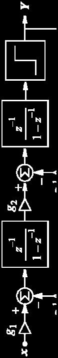
3 Overview of non-idealities Depending on the building-block: Fully-diff SC schematic of a 2nd-order M Clock: - Jitter Amplifiers: -Output swing -DC gain - Dynamic limitations (GB, SR) - Thermal and 1/f noise - Gain non-linearity Capacitors: -Mismatch - Non-linearity Switches: - Finite on-resistance - Thermal noise - Charge injection - Clock feedthrough - Non-linearity Comparators: -Hysteresis -Offset References: - Thermal and 1/f noise - Output impedance Multi-bit ADCs & DACs: -Gain error -Offset error - Non-linearity 3


4 Overview of non-idealities Depending on their effect: ERRORS DEGRADING NTF AMPLIFIER DC GAIN CAPACITOR MISMATCH INTEGRATOR SETTLING Amplifier GB Amplifier SR Switch R on Impact depends on topology Output PSD 4th order SINGLE-LOOP Ms Low sensitivity 3rd order CASCADE Ms Noise leakages Imperfect cancellation of low-order quantization errors 0.5/OSR 0.5 2nd order 1st order f/f s (log) 4
 INTEGRATOR SETTLING Amplifier GB CLOCK JITTER Amplifier SR DISTORTION Switch R on Non-linear amplifier gain Non-linear capacitors Impact depends on topology SINGLE-LOOP LOOP Ms")
5 Overview of non-idealities Depending on their effect: ERRORS DEGRADING NTF MODELED AS ADDITIVE ERRORS AMPLIFIER DC GAIN CIRCUIT NOISE CAPACITOR MISMATCH Thermal noise (switches, opamps, refs) 1/f noise (opamps, refs) INTEGRATOR SETTLING Amplifier GB CLOCK JITTER Amplifier SR DISTORTION Switch R on Non-linear amplifier gain Non-linear capacitors Impact depends on topology SINGLE-LOOP LOOP Ms Low sensitivity CASCADE Ms Noise leakages Imperfect cancellation of low-order quantization errors Non-linear settling Non-linear switches Front-end dominates Similar impact on different topologies 5


6 Integrator leakage Effect of amplifier gain on the integrator transfer function: Ideal SC integrator SC integrator considering amplifier finite gain g C C 1 2 Amplifier gain Shift of the pole from DC (z = 1) 6


7 Integrator leakage Effect on single-loop loop Ms: d ll -Ideally: -In practice: 2nd-order M Lth-order M: Quite insensitive to leakages ( 2, L-1 shaping) 7


8 Integrator leakage Effect on cascade Ms: M Mismatch between analog and digital filtering - Ideally: - In practice: low-order order leakages (L 1-1, L 2-1, ) 8
9 Integrator leakage Comparison of integrator leakage effect on 4th-order Ms (ideal) Sensitivity to int. leakages of cascades increases with OSR and L 1st-stage leakages dominate (L 1-1 shaping) 9


10 Capacitor mismatch Circuit primitive: Physical implementations: MOS cap Analog CMOS Digital CMOS Mixed CMOS 10


11 Capacitor mismatch Local and global errors in: Area Capacitance per Unit Area SC integrator t g C C 1 2 nc mc u u g g 1 1 n m C Cu u C ~ 0.05% 05% - 01% 0.1% using good quality caps and adequate layout strategies Centroid techniques 11


12 Capacitor mismatch Effect on single-loop loop Ms: - Ideally: 2nd-order M - In practice: Slight increase of error, but shaping is preserved 12


13 Capacitor mismatch Effect on cascade Ms: M - Ideally: - In practice: Mismatch between analog and digital it coeffs low-order leakages (L 1, L 2, ) 13


 32)")
14 Capacitor mismatch Effect on cascade Ms: C = 0.5% C = 0.1% M M (OSR = 32) (OSR = 32) 14


 -")

15 Capacitor mismatch Effect on cascade Ms: Required C for 1-bit loss in DR Sensitivity to mismatch rapidly increases with: - Oversampling ratio (OSR) - Cascade order (L) 1st-stage leakages 1st stage leakages dominate (L 1 shaping) 15


16 Integrator incomplete settling The relationship between opamp input and output is nonlinear and dynamic Settling error A DC GB, SR Integrator temporal evolution Integrator temporal evolution error due to amplifier finite bandwidth slew-rate limitation Modulator output spectrum increase on the noise floor harmonic distortion due to slewing SNDR degradation 16
17 Integrator incomplete settling Integrator temporal evolution: [Rio00] Both integration and sampling dynamics considered 1 pole model + SR limitation in amplifiers All parasitic caps taken into account 17


18 Integrator incomplete settling Integrator temporal evolution: [Rio00] Linear Partial Full response slew GB i SR i 18
19 Integrator incomplete settling Integrator temporal evolution: [Rio00] GB i GB s SR i SR s 19
20 Integrator incomplete settling Integrator temporal evolution: [Rio00] 20


21 Integrator incomplete settling Effect of the amplifier GB: If only amplifier GB is considered (assuming no SR limitation) - Can be viewed as a systematic error in the integrator weight - Effect on Ms similar to a mismatch between analog and digital coeffs l - It causes low-order noise leakages in cascade Ms 21


22 Integrator incomplete settling Additional effect of the amplifier SR (+ GB): - Dominant linear dynamics are not mandatory in order to fulfill specs - SR can be traded for GB - It can be used to optimize the power consumption of amplifiers Non-linear dynamics cause distortion! SR at the front-end integ must be carefully tackled 22


23 Integrator incomplete settling Additional effect of the switches Ron (+ GB + SR): = 1 Input is sampled with an error Linear dynamics are slowed down Slew time shortens 23


24 Circuit noise Main noise sources in SC integrators: Switches Thermal noise Amplifiers Thermal and flicker noise References Thermal and flicker noise Sampling: Integration: Noise contribution ti of the switches (input-referred): Switches for sampling Aliased component [Fisc82] C S = 0.66pF f s = 70MHz 24


:")

25 Circuit noise Main noise sources in SC integrators: Switches Thermal noise Amplifiers Thermal and flicker noise References Thermal and flicker noise Sampling: Integration: Noise contribution of the switches (input-referred): Switches for sampling Switches for integration 25

:")


26 Circuit noise Noise contribution of the amplifier (input-referred): Thermal + Flicker Thermal component corner freq. Aliased component Flicker component Low-pass filtered version at the integ input: Folded tails are submerged into the aliased thermal noise Similar treatment for the references 26
27 Circuit noise Total noise PSD for the front-end integ: switches amplifier references Switches: - kt/c is the ultimate limitation on the converter resolution - It can only be decreased by increasing Cs and/or fs (it does not depend on Ron!) - x2 in fully-diff implementations (3-dB increase, but signal power is 6dB larger!) Amplifiers & References: - GBs should be as low as settling errors allow (reduces folding!) - 1/f contributions decrease with the corner frequency - Adequate techniques can be applied in low-freq apps: CDS, chopper, [Enz96] In-band error power due to circuit noise in the M 27
28 Circuit noise Effect of noise leakages and thermal noise on a 2-1 cascade 3rd-order shaping w/ Thermal noise 2nd-order shaping no shaping w/ Integ leakage Ideal 28


29 Circuit noise Effect of 1/f and thermal noise on the spectra of a 4th-order M (silicon results for several fs) Thermal components Be careful with Flicker models for transistors! Front-end amplifier needed redesign! Flicker component (1/f) 29


30 Clock jitter Sampling time uncertainty [Boser88]: Non-uniform sampling of the input If jitter is modeled as random: Ideal J = 0.1ns, f x = 125kHz J = 0.1ns, f x = 500kHz Error is larger, the larger input freq (wideband apps!) 30


31 Non-linearity of capacitors In an ideal capacitor: dq = Cdv In practice: dq = C(v)dv, with C being voltage-dependent v i Considering the effect of the sampling cap only [Bran97]: a 1 = 500ppm/V, a 2 = 500ppm/V 2 HD 3 = -94.0dB HD 3 = -89.9dB HD 3 = -89.8dB - Even-order distortion cancels w/ fully-diff - Non-linearity of sampling cap dominates - Valid for weak non-linearities (MOS caps are very non-linear!) 31


32 Non-linear Amplifier Gain Actual amplifier gain depends on output voltage: Amplifier gain, db A DC Output voltage, V A DC = 500, 1 = 10%/V (single-ended M) [Yin94] - Increasing A DC helps a lot! - A DC at the front-end larger than noise leakages require 32


33 Non-linear settling SR can trade for GB in the integrator settling, but non-linear dynamics cause distortion: SR at the front-end larger than settling requires 33


34 Non-linear switch resistance Switches exhibit a finite R ON which is also non-linear: R ON, p R 1 ON, n R ON, n R ON, p W k' n ( V L n 1 W k' p ( v L p DD I v V V I Tp ) Tn ) R ON,eq V DD 0 VTp VDD VTn v I R R // R ON,eq ON, n ON, p Non-linear sampling [Geer02]: Alternative switch sizings Numerically solved - Distortion is dynamic (increases with input freq!) - Front-end switch dominates - R ON at the front-end smaller than settling requires - Very important in low-voltage! Most suited sizing i depends d on parasitics, Vref/Vsupply, 34


![similarly to quantization error [Boser88] P h](/docs-images/91/106082412/images/35-5.jpg "4h 2 2L π (2 L+1) OSR 2L 1 Effect of DAC")


35 Comparators and multi-bit quantizers Single-bit Ms: Multi-bit Ms: Comparator: 1-bit DAC Inherently linear Offset Attenuated by the integrator DC gain Hysteresis Shaped similarly to quantization error [Boser88] P h 4h 2 2L π (2 L+1) OSR 2L 1 Effect of DAC errors on a 2nd-order 3-bit M Multi-bit ADC Errors attenuated/shaped Multi-bit DAC Non-linearity directly added to the input! [Mede99]: σ D INL B LSB DEM techniques Dual quantization 35


.")

.")


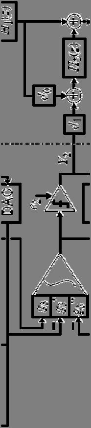
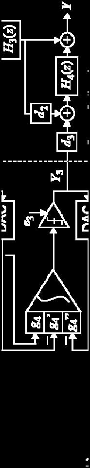
36 Case study A2.5-V Cascade SDM in CMOS 0.25um for ADSL/ADSL w/ dual quantization Two different amplifiers: 2-stage OA in the 1st stage, and 1-stage OA in 2nd and 3rd stages. Standard CMOS switches (no clock-boosting). Only 2-branch integrators and 2x16 unit capacitors (MiM). Comparators: regenerative latch + preamplification stage. 3-bit quantizer in the last stage: Resistive-ladder DAC (no calibration). Flash ADC: Static differential input stage + latched comparators. Power-down control. 36
37 Case study - Blocks Specs Blocks Specs EQUATION DATABASE Typical Worst Case Quantization noise -88.1dB -86.2dB MODULATOR Topology Oversampling ratio Reference voltage Clock Coc frequency Clock jitter Sampling capacitor 2-1-1(3b) 1(3b) V 70.4MHz 15ps (0.1%) 0.66pF Ideal Corner analysis: -90.3dB Cap. sigma (MiM, 1pF) 0.05% FRONT-END DC gain leakage Fast and slow devices models -99.8dB Cap. tolerance ±20% INTEGRATOR Cap. mismatch Temperature leakage range: [-40ºC, +110ºC] Bottom parasitic cap. 1% -95.4dB -89.4dB ( C = 0.05% ±5% 0.1%) variation in the 2.5-V supply Switch on-resistance 150 DAC error -96.4dB DC gain 3000 (70dB) GB (1.5pF) 265MHz Thermal noise -84.8dB -82.2dB AMPLIFIER Slew rate (1.5pF) 800V/ s kt/c noise -88.1dB -86.0dB Output swing ±1.8V Amplifier noise -87.5dB -84.5dB Input equivalent noise 6nV/sqrt(Hz) Clock jitter In-band error power Dynamic range -82.3dB 82.8dB (13.5bit) -90.1dB -80.3dB 80.8dB (13.1bit) COMPARATORS 3-bit QUANTIZER Hysteresis Offset Resolution time DAC INL 20mV ±10mV 3ns 0.5%FS 37
38 Case study MODULATOR Topology Oversampling ratio Reference voltage 2-1-1(3b) V Typical Worst Case Clock frequency Clock jitter 70.4MHz 15ps (0.1%) Quantization noise -88.1dB -86.2dB Sampling capacitor 0.66pF Ideal DC gain leakage Cap. mismatch leakage ( C = 0.05% 05% 0.1%) -90.3dB -99.8dB -95.4dB -89.4dB FRONT-END INTEGRATOR Cap. sigma (MiM, 1pF) Cap. tolerance Bottom parasitic cap. Switch on-resistance 0.05% ±20% 1% 150 DAC error -96.4dB Thermal noise -84.8dB -82.2dB kt/c noise -88.1dB -86.0dB AMPLIFIER DC gain GB (1.5pF) Slew rate (1.5pF) Output swing 3000 (70dB) 265MHz 800V/ s ±1.8V Amplifier noise -87.5dB -84.5dB Input equivalent noise 6nV/sqrt(Hz) Clock jitter -90.1dB Hysteresis 20mV In-band error power -82.3dB -80.3dB COMPARATORS Offset ±10mV Dynamic range 82.8dB (13.5bit) 80.8dB (13.1bit) 3-bit QUANTIZER Resolution time DAC INL 3ns 0.5%FS 38

.")


 Slew rate must be")

39 Case study - Integrator Dynamics Integrator Dynamics GB > 2.5f s is ideally enough to limit settling errors (this architecture w/ OSR = 16). Switch on-resistance slows down the effective amplifier response: R on ~ 150 requires just GB > 3.2f s Standard switches GB = 265MHz (no clock-boosting) (assuming that 85% of the clock cycle is useful) Slew rate must be large enough to let the linear dynamic to correctly settle. 6.5 SR = 800V/ s Partially slew-rate limited operation of the front-end integrator introduces distortion. 39
40 Case study - Amplifiers INTEG. 11 INTEG. 2 INTEG. 3 INTEG. 4 Unit capacitor 0.66pF 0.45pF 0.45pF SC CMFB nets DC gain (70dB) (70dB) 600 (56dB) pmos input scheme GB (1.5pF) 265MHz 265MHz 210MHz Slew rate (1.5pF) Output swing 800V/ s 800V/ s ±1.80V ±1.80V 350V/ s ±1.60V Cancelled body effect (substrate noise coupling) Smaller 1/f noise Input equivalent noise 6nV/sqrt(Hz) 50nV/sqrt(Hz) OPA OPB 40
41 Case study - Amplifiers INTEG. 1 INTEG. 2 INTEG. 3 INTEG. 4 Unit capacitor 0.66pF 0.45pF 0.45pF SC CMFB nets DC gain 3000 (70dB) 600 (56dB) pmos input scheme e GB (1.5pF) Slew rate (1.5pF) 265MHz 800V/ s 210MHz 350V/ s Cancelled body effect (substrate noise coupling) Output swing ±1.80V ±1.60V Smaller 1/f noise Input equivalent noise 6nV/sqrt(Hz) 50nV/sqrt(Hz) OPA 2-stage amplifier Telescopic 1st stage 2-path compensation DC gain GB (1.5pF) PM (1.5pF) SR (1.5pF) Output swing Input eq. noise Input capacitance Power consumption Typical 78.6dB 446.8MHz 64.0º 1059V/ s ±2.09V 5.1nV/sqrt(Hz) 126fF 17.2mW Worst Case 73.5dB 331.5MHz 57.9º 883V/ s ±1.86V 5.5nV/sqrt(Hz) 129fF 19.4mW 41


 Slew rate (1.")


")

 Output swing Input eq.")

 300fF 6.")
42 Case study - Amplifiers INTEG. 1 INTEG. 2 INTEG. 3 INTEG. 4 Unit capacitor 0.66pF 0.45pF 0.45pF SC CMFB nets DC gain 3000 (70dB) 600 (56dB) pmos input scheme GB (1.5pF) Slew rate (1.5pF) 265MHz 800V/ s 210MHz 350V/ s Cancelled body effect (substrate noise coupling) Output swing ±1.80V ±1.60V Smaller 1/f noise Input equivalent noise 6nV/sqrt(Hz) 50nV/sqrt(Hz) OPB folded-cascode amplifier DC gain GB (1.5pF) PM (1.5pF) SR (1.5pF) Output swing Input eq. noise Input capacitance Power consumption Typical 58.0dB 393.5MHz 70.3º 377V/ s ±1.97V 4.1nV/sqrt(Hz) 300fF 6.6mW Worst Case 56.8dB 331.7MHz 67.7º 373V/ s ±1.72V 5.1nV/sqrt(Hz) 343fF 6.9mW 42


43 Case study - Switch ON-Resistance Slow-down of the integrators dynamics Incomplete sampling (RC time constant) Dynamic distortion (front-end integrator) R on ~ 150 Standard CMOS switches nmos: 8.5/0.25 pmos: 36.5/0.25 No clock-boosting No low-vt transistors 43


44 Case study - Switch ON-Resistance Dynamic distortion evaluated through electrical simulation 366kHz Sinewave input DMT input 44

 Very good matching (0.")


45 Case study - MiM Capacitors CMOS tech with mixed-signal facilities M5 thin oxide Thin oxide between M4 metal 4 and metal 5 TOP BOTTOM M3 Cap. matching 0.05% (1pF) Very good matching (0.1% assumed for 6- design) Bottom plate parasitic 1% Helps to limit the capacitive load to integrators Cap. spread ±20% Integrators weights: Front-end integ, 0.66pF: 27 m x 27 m Remaining integs, 0.45pF: 22 m x 22 m Also MiM caps in OPA, in the SC CMFB nets, and in the anti-aliasing aliasing filter 45


 Unsalicided n+ poly used in")


46 Case study - Quantizers Comparator Pre-amp + Regenerative latch + SR latch (Different supplies) Hysteresis Resolution time, LH Input capacitance V 3.9ns 100fF Offset Resolution time, HL Power consumption 6.3mV 2.8ns 0.3mW 3-bit Quantizer Resistive-ladder DAC 700- ladder between references +2V/+0.5V (14x50, 3.21mW) Unsalicided n+ poly used in resistors References obtained from the on-chip analog supply Flash ADC Static input scheme (no caps) Reduces capacitive load to 4th integrator Saves silicon area Extra differential pair in comparators 46


47 Case study - Layout & Prototyping CMOS 0.25 m 2.78mm 2 w/o pads 44-pin plastic QFP 4-layer PCB Dedicated analog, mixed, and digital supplies Guard rings with dedicated pad/pin Increased distance among analog and digital blocks Layout symmetry and common-centroid techniques Shielded bus for distributing the clock signals Extensive on-chip decoupling Pad ring divided blocking cells Multiple bonding techniques 47


48 Case study - Experimental results 160kHz THD = -87dB SFDR = 90dB Part of a commercial modem In mass production (STMicroelectronics) 48
49 References [Boser88] B.E. Boser and B.A. Wooley, The Design of Sigma-Delta Modulation Analog-to-Digital Converters. IEEE Journal of Solid-State Circuits, vol. 23. pp , December [Bran97] [Enz96] B. Brandt, P.F. Ferguson, and M. Rebeschini, Analog Circuit Design of Σ ADCs, Chapter 11 in Delta-Sigma Data Converters: Theory, Design and Simulation (S.R. Norsworthy, R. Schreier, and G.C. Temes, Editors). IEEE Press, C.C. Enz and G.C. Temes, Circuit Techniques for Reducing the Effects of Op-Amp Imperfections: Autozeroing, Correlated Double Sampling, and Chopper Stabilization. Proceedings of the IEEE, vol. 84, no. 11, pp , November [Fisc82] J.H. Fischer, Noise Sources and Calculation Techniques for Switched Capacitor Filters. IEEE Journal of Solid-State Circuits, vol. 17, no. 4, pp , August [Geer02] Y. Geerts, M. Steyaert, and W. Sansen, Design of Multi-Bit Delta-Sigma A/D Converters. Kluwer Academic Publishers, [Mede99] F. Medeiro, B. Pérez-Verdú, and A. Rodríguez-Vázquez, Top-Down Design of High-Performance Modulators. Kluwer Academic Publishers, [Rio00] [Yin94] R. del Río, F. Medeiro, B. Pérez-Verdú, and A. Rodríguez-Vázquez, Reliable Analysis of Settling Errors in SC Integrators: Application to Σ Modulators. IEE Electronics Letters, vol. 36, no. 6, pp , March G. Yin and W. Sansen, A High-Frequency and High-Resolution Fourth-Order Σ A/D Converter in BiCMOS Technology. IEEE Journal of Solid-State Circuits, vol. 29, pp , August More details on errors and case study [Rio06] R. del Río, F. Medeiro, B. Pérez-Verdú, J.M. de la Rosa, and A. Rodríguez-Vázquez, CMOS Cascade Sigma- Delta Modulators for Sensors and Telecom: Error Analysis and Practical Design. Springer,
Basic Concepts and Architectures
 CMOS Sigma-Delta Converters From Basics to State-of of-the-art Basic Concepts and Architectures Rocío del Río, R Belén Pérez-Verdú and José M. de la Rosa {rocio,belen,jrosa}@imse.cnm.es KTH, Stockholm,
EE247 Lecture 24. EE247 Lecture 24
 EE247 Lecture 24 Administrative EE247 Final exam: Date: Wed. Dec. 15 th Time: -12:30pm-3:30pm- Location: 289 Cory Closed book/course notes No calculators/cell phones/pdas/computers Bring one 8x11 paper
DESIGN OF MULTI-BIT DELTA-SIGMA A/D CONVERTERS
 DESIGN OF MULTI-BIT DELTA-SIGMA A/D CONVERTERS DESIGN OF MULTI-BIT DELTA-SIGMA A/D CONVERTERS by Yves Geerts Alcatel Microelectronics, Belgium Michiel Steyaert KU Leuven, Belgium and Willy Sansen KU Leuven,
A 2.5 V 109 db DR ADC for Audio Application
 276 JOURNAL OF SEMICONDUCTOR TECHNOLOGY AND SCIENCE, VOL.10, NO.4, DECEMBER, 2010 A 2.5 V 109 db DR ADC for Audio Application Gwangyol Noh and Gil-Cho Ahn Abstract A 2.5 V feed-forward second-order deltasigma
Materials in this course have been contributed by Fernando Medeiro, José M. de la Rosa, Rocío del Río, Belén Pérez-Verdú and
 CMOS Sigma-Delta Converters From Basics to State-of-the-Art Circuits and Errors Angel Rodríguez-Vázquez angel@imse.cnm.es Barcelona, 29-30 / Septiembre / 2010 Materials in this course have been contributed
Architectures and Design Methodologies for Very Low Power and Power Effective A/D Sigma-Delta Converters
 0 Architectures and Design Methodologies for Very Low Power and Power Effective A/D Sigma-Delta Converters F. Maloberti University of Pavia - Italy franco.maloberti@unipv.it 1 Introduction Summary Sigma-Delta
Second-Order Sigma-Delta Modulator in Standard CMOS Technology
 SERBIAN JOURNAL OF ELECTRICAL ENGINEERING Vol. 1, No. 3, November 2004, 37-44 Second-Order Sigma-Delta Modulator in Standard CMOS Technology Dragiša Milovanović 1, Milan Savić 1, Miljan Nikolić 1 Abstract:
BandPass Sigma-Delta Modulator for wideband IF signals
 BandPass Sigma-Delta Modulator for wideband IF signals Luca Daniel (University of California, Berkeley) Marco Sabatini (STMicroelectronics Berkeley Labs) maintain the same advantages of BaseBand converters
SUPPORTED by a considerable commercial success, wireline
 IEEE TRANSACTIONS ON CIRCUITS AND SYSTEMS I: REGULAR PAPERS, VOL. 51, NO. 1, JANUARY 2004 47 Highly Linear 2.5-V CMOS 61 Modulator for ADSL+ Rocío del Río, José M. de la Rosa, Belén Pérez-Verdú, Manuel
Oversampling Converters
 Oversampling Converters Behzad Razavi Electrical Engineering Department University of California, Los Angeles Outline Basic Concepts First- and Second-Order Loops Effect of Circuit Nonidealities Cascaded
A Successive Approximation ADC based on a new Segmented DAC
 A Successive Approximation ADC based on a new Segmented DAC segmented current-mode DAC successive approximation ADC bi-direction segmented current-mode DAC DAC INL 0.47 LSB DNL 0.154 LSB DAC 3V 8 2MS/s
Publication [P3] By choosing to view this document, you agree to all provisions of the copyright laws protecting it.
![Publication [P3] By choosing to view this document, you agree to all provisions of the copyright laws protecting it.](/thumbs/94/120865947.jpg "Publication [P3] By choosing to view this document, you agree to all provisions of the copyright laws protecting it.") Publication [P3] Copyright c 2006 IEEE. Reprinted, with permission, from Proceedings of IEEE International Solid-State Circuits Conference, Digest of Technical Papers, 5-9 Feb. 2006, pp. 488 489. This
Publication [P3] Copyright c 2006 IEEE. Reprinted, with permission, from Proceedings of IEEE International Solid-State Circuits Conference, Digest of Technical Papers, 5-9 Feb. 2006, pp. 488 489. This
NPTEL. VLSI Data Conversion Circuits - Video course. Electronics & Communication Engineering.
 NPTEL Syllabus VLSI Data Conversion Circuits - Video course COURSE OUTLINE This course covers the analysis and design of CMOS Analog-to-Digital and Digital-to-Analog Converters,with about 7 design assigments.
EE247 Lecture 26. EE247 Lecture 26
 EE247 Lecture 26 Administrative EE247 Final exam: Date: Mon. Dec. 18 th Time: 12:30pm-3:30pm Location: 241 Cory Hall Extra office hours: Thurs. Dec. 14 th, 10:30am-12pm Closed book/course notes No calculators/cell
A PSEUDO-CLASS-AB TELESCOPIC-CASCODE OPERATIONAL AMPLIFIER
 A PSEUDO-CLASS-AB TELESCOPIC-CASCODE OPERATIONAL AMPLIFIER M. Taherzadeh-Sani, R. Lotfi, and O. Shoaei ABSTRACT A novel class-ab architecture for single-stage operational amplifiers is presented. The structure
Modulator with Op- Amp Gain Compensation for Nanometer CMOS Technologies
 A. Pena Perez, V.R. Gonzalez- Diaz, and F. Maloberti, ΣΔ Modulator with Op- Amp Gain Compensation for Nanometer CMOS Technologies, IEEE Proceeding of Latin American Symposium on Circuits and Systems, Feb.
NOISE IN SC CIRCUITS
 ECE37 Advanced Analog Circuits Lecture 0 NOISE IN SC CIRCUITS Richard Schreier richard.schreier@analog.com Trevor Caldwell trevor.caldwell@utoronto.ca Course Goals Deepen Understanding of CMOS analog circuit
Sigma-Delta ADC Tutorial and Latest Development in 90 nm CMOS for SoC
 Sigma-Delta ADC Tutorial and Latest Development in 90 nm CMOS for SoC Jinseok Koh Wireless Analog Technology Center Texas Instruments Inc. Dallas, TX Outline Fundamentals for ADCs Over-sampling and Noise
Data Conversion Techniques (DAT115)
") Data Conversion Techniques (DAT115) Hand in Report Second Order Sigma Delta Modulator with Interleaving Scheme Group 14N Remzi Yagiz Mungan, Christoffer Holmström [ 1 20 ] Contents 1. Task Description...
Data Conversion Techniques (DAT115) Hand in Report Second Order Sigma Delta Modulator with Interleaving Scheme Group 14N Remzi Yagiz Mungan, Christoffer Holmström [ 1 20 ] Contents 1. Task Description...
Advanced Analog Integrated Circuits. Precision Techniques
 Advanced Analog Integrated Circuits Precision Techniques Bernhard E. Boser University of California, Berkeley boser@eecs.berkeley.edu Copyright 2016 by Bernhard Boser 1 Topics Offset Drift 1/f Noise Mismatch
ECE 627 Project: Design of a High-Speed Delta-Sigma A/D Converter
 ECE 627 Project: Design of a High-Speed Delta-Sigma A/D Converter Brian L. Young youngbr@eecs.oregonstate.edu Oregon State University June 6, 28 I. INTRODUCTION The goal of the Spring 28, ECE 627 project
Low-Power Pipelined ADC Design for Wireless LANs
 Low-Power Pipelined ADC Design for Wireless LANs J. Arias, D. Bisbal, J. San Pablo, L. Quintanilla, L. Enriquez, J. Vicente, J. Barbolla Dept. de Electricidad y Electrónica, E.T.S.I. de Telecomunicación,
A 98dB 3.3V 28mW-per-channel multibit audio DAC in a standard 0.35µm CMOS technology
 A 98dB 3.3V 28mW-per-channel multibit audio DAC in a standard 0.35µm CMOS technology M. Annovazzi, V. Colonna, G. Gandolfi, STMicroelectronics Via Tolomeo, 2000 Cornaredo (MI), Italy vittorio.colonna@st.com
RELAXED TIMING ISSUE IN GLOBAL FEEDBACK PATHS OF UNITY- STF SMASH SIGMA DELTA MODULATOR ARCHITECTURE
 RELAXED TIMING ISSUE IN GLOBAL FEEDBACK PATHS OF UNITY- STF SMASH SIGMA DELTA MODULATOR ARCHITECTURE Mehdi Taghizadeh and Sirus Sadughi Department of Electrical Engineering, Science and Research Branch,
Design of Continuous Time Multibit Sigma Delta ADC for Next Generation Wireless Applications
 RESEARCH ARTICLE OPEN ACCESS Design of Continuous Time Multibit Sigma Delta ADC for Next Generation Wireless Applications Sharon Theresa George*, J. Mangaiyarkarasi** *(Department of Information and Communication
A Unity Gain Fully-Differential 10bit and 40MSps Sample-And-Hold Amplifier in 0.18μm CMOS
 A Unity Gain Fully-Differential 0bit and 40MSps Sample-And-Hold Amplifier in 0.8μm CMOS Sanaz Haddadian, and Rahele Hedayati Abstract A 0bit, 40 MSps, sample and hold, implemented in 0.8-μm CMOS technology
Low-power Sigma-Delta AD Converters
 Low-power Sigma-Delta AD Converters Willy Sansen KULeuven, ESAT-MICAS Leuven, Belgium willy.sansen@esat.kuleuven.be Willy Sansen 10-05 211 Table of contents Delta-sigma modulation The switch problem The
Design and Implementation of a Sigma Delta ADC By: Moslem Rashidi, March 2009
 Design and Implementation of a Sigma Delta ADC By: Moslem Rashidi, March 2009 Introduction The first thing in design an ADC is select architecture of ADC that is depend on parameters like bandwidth, resolution,
EE247 Lecture 26. This lecture is taped on Wed. Nov. 28 th due to conflict of regular class hours with a meeting
 EE47 Lecture 6 This lecture is taped on Wed. Nov. 8 th due to conflict of regular class hours with a meeting Any questions regarding this lecture could be discussed during regular office hours or in class
Integrated Microsystems Laboratory. Franco Maloberti
 University of Pavia Integrated Microsystems Laboratory Power Efficient Data Convertes Franco Maloberti franco.maloberti@unipv.it OUTLINE Introduction Managing the noise power budget Challenges of State-of-the-art
Two- Path Band- Pass Σ- Δ Modulator with 40- MHz IF 72- db DR at 1- MHz Bandwidth Consuming 16 mw
 I. Galdi, E. Bonizzoni, F. Maloberti, G. Manganaro, P. Malcovati: "Two-Path Band- Pass Σ-Δ Modulator with 40-MHz IF 72-dB DR at 1-MHz Bandwidth Consuming 16 mw"; 33rd European Solid State Circuits Conf.,
A 10 bit, 1.8 GS/s Time Interleaved Pipeline ADC
 A 10 bit, 1.8 GS/s Time Interleaved Pipeline ADC M. Åberg 2, A. Rantala 2, V. Hakkarainen 1, M. Aho 1, J. Riikonen 1, D. Gomes Martin 2, K. Halonen 1 1 Electronic Circuit Design Laboratory Helsinki University
CHAPTER. delta-sigma modulators 1.0
 CHAPTER 1 CHAPTER Conventional delta-sigma modulators 1.0 This Chapter presents the traditional first- and second-order DSM. The main sources for non-ideal operation are described together with some commonly
A 12-bit Interpolated Pipeline ADC using Body Voltage Controlled Amplifier
 A 12-bit Interpolated Pipeline ADC using Body Voltage Controlled Amplifier Hyunui Lee, Masaya Miyahara, and Akira Matsuzawa Tokyo Institute of Technology, Japan Outline Background Body voltage controlled
Advanced Operational Amplifiers
 IsLab Analog Integrated Circuit Design OPA2-47 Advanced Operational Amplifiers כ Kyungpook National University IsLab Analog Integrated Circuit Design OPA2-1 Advanced Current Mirrors and Opamps Two-stage
Lecture #6: Analog-to-Digital Converter
 Lecture #6: Analog-to-Digital Converter All electrical signals in the real world are analog, and their waveforms are continuous in time. Since most signal processing is done digitally in discrete time,
A Digitally Enhanced 1.8-V 15-b 40- Msample/s CMOS Pipelined ADC
 A Digitally Enhanced.8-V 5-b 4- Msample/s CMOS d ADC Eric Siragusa and Ian Galton University of California San Diego Now with Analog Devices San Diego California Outline Conventional PADC Example Digitally
Analog CMOS Interface Circuits for UMSI Chip of Environmental Monitoring Microsystem
 Analog CMOS Interface Circuits for UMSI Chip of Environmental Monitoring Microsystem A report Submitted to Canopus Systems Inc. Zuhail Sainudeen and Navid Yazdi Arizona State University July 2001 1. Overview
Design of a Sample and Hold Circuit using Rail to Rail Low Voltage Compact Operational Amplifier and bootstrap Switching
 RESEARCH ARTICLE OPEN ACCESS Design of a Sample and Hold Circuit using Rail to Rail Low Voltage Compact Operational Amplifier and bootstrap Switching Annu Saini, Prity Yadav (M.Tech. Student, Department
Revision History. Contents
 Revision History Ver. # Rev. Date Rev. By Comment 0.0 9/15/2012 Initial draft 1.0 9/16/2012 Remove class A part 2.0 9/17/2012 Comments and problem 2 added 3.0 10/3/2012 cmdmprobe re-simulation, add supplement
MASH 2-1 MULTI-BIT SIGMA-DELTA MODULATOR FOR WLAN L 2 ( ) ( ) 1( 1 1 1
 ( ) 1( 1 1 1") MASH 2- MULTI-BIT SIGMA-DELTA MODULATOR FOR WLAN Yu hang, Ning Xie, Hui Wang and Yejun He College of Information Engineering, Shenzhen University, Shenzhen, Guangdong 58060, China kensouren@yahoo.com.cn
MASH 2- MULTI-BIT SIGMA-DELTA MODULATOR FOR WLAN Yu hang, Ning Xie, Hui Wang and Yejun He College of Information Engineering, Shenzhen University, Shenzhen, Guangdong 58060, China kensouren@yahoo.com.cn
HIGH-SPEED bandpass modulators are desired in
 IEEE TRANSACTIONS ON CIRCUITS AND SYSTEMS II: ANALOG AND DIGITAL SIGNAL PROCESSING, VOL. 45, NO. 5, MAY 1998 547 A 160-MHz Fourth-Order Double-Sampled SC Bandpass Sigma Delta Modulator Seyfi Bazarjani,
Oversampling Data Converters Tuesday, March 15th, 9:15 11:40
 Oversampling Data Converters Tuesday, March 15th, 9:15 11:40 Snorre Aunet (sa@ifi.uio.no) Nanoelectronics group Department of Informatics University of Oslo Last time and today, Tuesday 15th of March:
CMOS High Speed A/D Converter Architectures
 CHAPTER 3 CMOS High Speed A/D Converter Architectures 3.1 Introduction In the previous chapter, basic key functions are examined with special emphasis on the power dissipation associated with its implementation.
Tuesday, March 22nd, 9:15 11:00
 Nonlinearity it and mismatch Tuesday, March 22nd, 9:15 11:00 Snorre Aunet (sa@ifi.uio.no) Nanoelectronics group Department of Informatics University of Oslo Last time and today, Tuesday 22nd of March:
Design of Miller Compensated Two-Stage Operational Amplifier for Data Converter Applications
 Design of Miller Compensated Two-Stage Operational Amplifier for Data Converter Applications Prema Kumar. G Shravan Kudikala Casest, School Of Physics Casest, School Of Physics University Of Hyderabad
A Novel Continuous-Time Common-Mode Feedback for Low-Voltage Switched-OPAMP
 10.4 A Novel Continuous-Time Common-Mode Feedback for Low-oltage Switched-OPAMP M. Ali-Bakhshian Electrical Engineering Dept. Sharif University of Tech. Azadi Ave., Tehran, IRAN alibakhshian@ee.sharif.edu
INF4420 Switched capacitor circuits Outline
 INF4420 Switched capacitor circuits Spring 2012 1 / 54 Outline Switched capacitor introduction MOSFET as an analog switch z-transform Switched capacitor integrators 2 / 54 Introduction Discrete time analog
ISSCC 2004 / SESSION 25 / HIGH-RESOLUTION NYQUIST ADCs / 25.4
 ISSCC 2004 / SESSION 25 / HIGH-RESOLUTION NYQUIST ADCs / 25.4 25.4 A 1.8V 14b 10MS/s Pipelined ADC in 0.18µm CMOS with 99dB SFDR Yun Chiu, Paul R. Gray, Borivoje Nikolic University of California, Berkeley,
A 16Ω Audio Amplifier with 93.8 mw Peak loadpower and 1.43 quiscent power consumption
 A 16Ω Audio Amplifier with 93.8 mw Peak loadpower and 1.43 quiscent power consumption IEEE Transactions on circuits and systems- Vol 59 No:3 March 2012 Abstract A class AB audio amplifier is used to drive
A 4 GSample/s 8-bit ADC in. Ken Poulton, Robert Neff, Art Muto, Wei Liu, Andrew Burstein*, Mehrdad Heshami* Agilent Laboratories Palo Alto, California
 A 4 GSample/s 8-bit ADC in 0.35 µm CMOS Ken Poulton, Robert Neff, Art Muto, Wei Liu, Andrew Burstein*, Mehrdad Heshami* Agilent Laboratories Palo Alto, California 1 Outline Background Chip Architecture
MODELING BAND-PASS SIGMA-DELTA MODULATORS IN SIMULINK
 Vienna, AUSTRIA, 000, Septemer 5-8 MODELING BAND-PASS SIGMA-DELTA MODULATORS IN SIMULINK S. Brigati (), F. Francesconi (), P. Malcovati () and F. Maloerti (3) () Dep. of Electrical Engineering, University
Appendix A Comparison of ADC Architectures
 Appendix A Comparison of ADC Architectures A comparison of continuous-time delta-sigma (CT ), pipeline, and timeinterleaved (TI) SAR ADCs which target wide signal bandwidths (greater than 100 MHz) and
Noise George Yuan Hong Kong University of Science and Technology Fall 2010
 Lecture 3 Noise George Yuan Hong Kong University of Science and Technology Fall 2010 1 Outline Introduction Device noise models Circuit noise analysis Other noise sources Power noise Substrate noise Noise
DAT175: Topics in Electronic System Design
 DAT175: Topics in Electronic System Design Analog Readout Circuitry for Hearing Aid in STM90nm 21 February 2010 Remzi Yagiz Mungan v1.10 1. Introduction In this project, the aim is to design an adjustable
2246 IEEE JOURNAL OF SOLID-STATE CIRCUITS, VOL. 40, NO. 11, NOVEMBER 2005
 2246 IEEE JOURNAL OF SOLID-STATE CIRCUITS, VOL. 40, NO. 11, NOVEMBER 2005 A CMOS 110-dB@40-kS/s Programmable-Gain Chopper-Stabilized Third-Order 2-1 Cascade Sigma-Delta Modulator for Low-Power High-Linearity
A 25MS/s 14b 200mW Σ Modulator in 0.18µm CMOS
 UT Mixed-Signal/RF Integrated Circuits Seminar Series A 25MS/s 14b 200mW Σ Modulator in 0.18µm CMOS Pio Balmelli April 19 th, Austin TX 2 Outline VDSL specifications Σ A/D converter features Broadband
A new class AB folded-cascode operational amplifier
 A new class AB folded-cascode operational amplifier Mohammad Yavari a) Integrated Circuits Design Laboratory, Department of Electrical Engineering, Amirkabir University of Technology, Tehran, Iran a) myavari@aut.ac.ir
Design of High-Speed Op-Amps for Signal Processing
 Design of High-Speed Op-Amps for Signal Processing R. Jacob (Jake) Baker, PhD, PE Professor and Chair Boise State University 1910 University Dr. Boise, ID 83725-2075 jbaker@ieee.org Abstract - As CMOS
INF4420. Switched capacitor circuits. Spring Jørgen Andreas Michaelsen
 INF4420 Switched capacitor circuits Spring 2012 Jørgen Andreas Michaelsen (jorgenam@ifi.uio.no) Outline Switched capacitor introduction MOSFET as an analog switch z-transform Switched capacitor integrators
INF4420. ΔΣ data converters. Jørgen Andreas Michaelsen Spring 2012
 INF4420 ΔΣ data converters Spring 2012 Jørgen Andreas Michaelsen (jorgenam@ifi.uio.no) Outline Oversampling Noise shaping Circuit design issues Higher order noise shaping Introduction So far we have considered
Op-Amp Design Project EE 5333 Analog Integrated Circuits Prof. Ramesh Harjani Department of ECE University of Minnesota, Twin Cities Report prepared
 Op-Amp Design Project EE 5333 Analog Integrated Circuits Prof. Ramesh Harjani Department of ECE University of Minnesota, Twin Cities Report prepared by: Nirav Desai (4280229) 1 Contents: 1. Design Specifications
Final Exam Spring 2012
 1 EE 435 Final Exam Spring 2012 Name Instructions: This is an open-book, open-notes, open computer exam but no collaboration either personal or electronic with anyone except the course instructor is permitted.
Overcoming Offset. Prof. Kofi Makinwa. Electronic Instrumentation Laboratory / DIMES Delft University of Technology Delft, The Netherlands
 Overcoming Offset Prof. Kofi Makinwa Electronic Instrumentation Laboratory / DIMES Delft University of Technology Delft, The Netherlands email: k.a.a.makinwa@tudelft.nl Motivation The offset of amplifiers
The Case for Oversampling
 EE47 Lecture 4 Oversampled ADCs Why oversampling? Pulse-count modulation Sigma-delta modulation 1-Bit quantization Quantization error (noise) spectrum SQNR analysis Limit cycle oscillations nd order ΣΔ
Lecture 3 Switched-Capacitor Circuits Trevor Caldwell
 Advanced Analog Circuits Lecture 3 Switched-Capacitor Circuits Trevor Caldwell trevor.caldwell@analog.com Lecture Plan Date Lecture (Wednesday 2-4pm) Reference Homework 2017-01-11 1 MOD1 & MOD2 ST 2, 3,
CMOS ADC & DAC Principles
 CMOS ADC & DAC Principles Willy Sansen KULeuven, ESAT-MICAS Leuven, Belgium willy.sansen@esat.kuleuven.be Willy Sansen 10-05 201 Table of contents Definitions Digital-to-analog converters Resistive Capacitive
A 1.8-V 16 Modulator Interface for an Electret Microphone With On-Chip Reference
 IEEE JOURNAL OF SOLID-STATE CIRCUITS, VOL. 37, NO. 3, MARCH 2002 279 A 1.8-V 16 Modulator Interface for an Electret Microphone With On-Chip Reference Ovidiu Bajdechi, Student Member, IEEE, and Johan H.
Fractional- N PLL with 90 Phase Shift Lock and Active Switched- Capacitor Loop Filter
 J. Park, F. Maloberti: "Fractional-N PLL with 90 Phase Shift Lock and Active Switched-Capacitor Loop Filter"; Proc. of the IEEE Custom Integrated Circuits Conference, CICC 2005, San Josè, 21 September
Operational Amplifier with Two-Stage Gain-Boost
 Proceedings of the 6th WSEAS International Conference on Simulation, Modelling and Optimization, Lisbon, Portugal, September 22-24, 2006 482 Operational Amplifier with Two-Stage Gain-Boost FRANZ SCHLÖGL
CHAPTER 3 DESIGN OF PIPELINED ADC USING SCS-CDS AND OP-AMP SHARING TECHNIQUE
 CHAPTER 3 DESIGN OF PIPELINED ADC USING SCS-CDS AND OP-AMP SHARING TECHNIQUE 3.1 INTRODUCTION An ADC is a device which converts a continuous quantity into discrete digital signal. Among its types, pipelined
Analog Integrated Circuits. Lecture 7: OpampDesign
 Analog Integrated Circuits Lecture 7: OpampDesign ELC 601 Fall 2013 Dr. Ahmed Nader Dr. Mohamed M. Aboudina anader@ieee.org maboudina@gmail.com Department of Electronics and Communications Engineering
Low-Voltage Low-Power Switched-Current Circuits and Systems
 Low-Voltage Low-Power Switched-Current Circuits and Systems Nianxiong Tan and Sven Eriksson Dept. of Electrical Engineering Linköping University S-581 83 Linköping, Sweden Abstract This paper presents
ISSCC 2006 / SESSION 16 / MEMS AND SENSORS / 16.1
 16.1 A 4.5mW Closed-Loop Σ Micro-Gravity CMOS-SOI Accelerometer Babak Vakili Amini, Reza Abdolvand, Farrokh Ayazi Georgia Institute of Technology, Atlanta, GA Recently, there has been an increasing demand
Analog-to-Digital Converters
 EE47 Lecture 3 Oversampled ADCs Why oversampling? Pulse-count modulation Sigma-delta modulation 1-Bit quantization Quantization error (noise) spectrum SQNR analysis Limit cycle oscillations nd order ΣΔ
IOWA STATE UNIVERSITY. EE501 Project. Fully Differential Multi-Stage Op-Amp Design. Ryan Boesch 11/12/2008
 IOWA STATE UNIVERSITY EE501 Project Fully Differential Multi-Stage Op-Amp Design Ryan Boesch 11/12/2008 This report documents the design, simulation, layout, and post-layout simulation of a fully differential
EE247 Lecture 27. EE247 Lecture 27
 EE247 Lecture 27 Administrative EE247 Final exam: Date: Wed. Dec. 19 th Time: 12:30pm-3:30pm Location: 70 Evans Hall Extra office hours: Thurs. Dec. 13 th, 10:am2pm Closed course notes/books No calculators/cell
A Low-Noise Self-Calibrating Dynamic Comparator for High-Speed ADCs
 1 A Low-Noise Self-Calibrating Dynamic Comparator for High-Speed ADCs Masaya Miyahara, Yusuke Asada, Daehwa Paik and Akira Matsuzawa Tokyo Institute of Technology, Japan Outline 2 Motivation The Calibration
Design of Analog and Mixed Integrated Circuits and Systems Theory Exercises
 102726 Design of nalog and Mixed Theory Exercises Francesc Serra Graells http://www.cnm.es/~pserra/uab/damics paco.serra@imb-cnm.csic.es 1 Introduction to the Design of nalog Integrated Circuits 1.1 The
METHODOLOGY FOR THE DIGITAL CALIBRATION OF ANALOG CIRCUITS AND SYSTEMS
 METHODOLOGY FOR THE DIGITAL CALIBRATION OF ANALOG CIRCUITS AND SYSTEMS METHODOLOGY FOR THE DIGITAL CALIBRATION OF ANALOG CIRCUITS AND SYSTEMS with Case Studies by Marc Pastre Ecole Polytechnique Fédérale
Summary Last Lecture
 Interleaved ADCs EE47 Lecture 4 Oversampled ADCs Why oversampling? Pulse-count modulation Sigma-delta modulation 1-Bit quantization Quantization error (noise) spectrum SQNR analysis Limit cycle oscillations
Cascaded Noise Shaping for Oversampling A/D and D/A Conversion Bruce A. Wooley Stanford University
 Cascaded Noise Shaping for Oversampling A/D and D/A Conversion Bruce A. Wooley Stanford University Bruce A. Wooley - 1 - Copyright 2005, Stanford University Outline Oversampling modulators for A-to-D conversion
Design of Pipeline Analog to Digital Converter
 Design of Pipeline Analog to Digital Converter Vivek Tripathi, Chandrajit Debnath, Rakesh Malik STMicroelectronics The pipeline analog-to-digital converter (ADC) architecture is the most popular topology
444 Index. F Fermi potential, 146 FGMOS transistor, 20 23, 57, 83, 84, 98, 205, 208, 213, 215, 216, 241, 242, 251, 280, 311, 318, 332, 354, 407
 Index A Accuracy active resistor structures, 46, 323, 328, 329, 341, 344, 360 computational circuits, 171 differential amplifiers, 30, 31 exponential circuits, 285, 291, 292 multifunctional structures,
TWO AND ONE STAGES OTA
 TWO AND ONE STAGES OTA F. Maloberti Department of Electronics Integrated Microsystem Group University of Pavia, 7100 Pavia, Italy franco@ele.unipv.it tel. +39-38-50505; fax. +39-038-505677 474 EE Department
Dynamically Reconfigurable Sensor Electronics Concept, Architecture, First Measurement Results, and Perspective
 Institute of Integrated Sensor Systems Dept. of Electrical Engineering and Information Technology Dynamically Reconfigurable Sensor Electronics Concept, Architecture, First Measurement Results, and Perspective
A 102-dB-SNR mixed CT/DT ADC with capacitor digital self-calibration for RC spread compensation
 Vol. 32, No. 8 Journal of Semiconductors August 2011 A 102-dB-SNR mixed CT/DT ADC with capacitor digital self-calibration for RC spread compensation Liu Yan( 刘岩 ), Hua Siliang( 华斯亮 ), Wang Donghui( 王东辉
On the Study of Improving Noise Shaping Techniques in Wide Bandwidth Sigma Delta Modulators
 On the Study of Improving Noise Shaping Techniques in Wide Bandwidth Sigma Delta Modulators By Du Yun Master Degree in Electrical and Electronics Engineering 2013 Faculty of Science and Technology University
ECE626 Project Switched Capacitor Filter Design
 ECE626 Project Switched Capacitor Filter Design Hari Prasath Venkatram Contents I Introduction 2 II Choice of Topology 2 III Poles and Zeros 2 III-ABilinear Transform......................................
EE247 Lecture 17. EECS 247 Lecture 17: Data Converters 2006 H.K. Page 1. Summary of Last Lecture
 EE47 Lecture 7 DAC Converters (continued) DAC dynamic non-idealities DAC design considerations Self calibration techniques Current copiers Dynamic element matching DAC reconstruction filter ADC Converters
ALTHOUGH zero-if and low-if architectures have been
 IEEE JOURNAL OF SOLID-STATE CIRCUITS, VOL. 40, NO. 6, JUNE 2005 1249 A 110-MHz 84-dB CMOS Programmable Gain Amplifier With Integrated RSSI Function Chun-Pang Wu and Hen-Wai Tsao Abstract This paper describes
Summary 185. Chapter 4
 Summary This thesis describes the theory, design and realization of precision interface electronics for bridge transducers and thermocouples that require high accuracy, low noise, low drift and simultaneously,
Tones. EECS 247 Lecture 21: Oversampled ADC Implementation 2002 B. Boser 1. 1/512 1/16-1/64 b1. 1/10 1 1/4 1/4 1/8 k1z -1 1-z -1 I1. k2z -1.
 Tones 5 th order Σ modulator DC inputs Tones Dither kt/c noise EECS 47 Lecture : Oversampled ADC Implementation B. Boser 5 th Order Modulator /5 /6-/64 b b b b X / /4 /4 /8 kz - -z - I kz - -z - I k3z
IN the design of the fine comparator for a CMOS two-step flash A/D converter, the main design issues are offset cancelation
 JOURNAL OF STELLAR EE315 CIRCUITS 1 A 60-MHz 150-µV Fully-Differential Comparator Erik P. Anderson and Jonathan S. Daniels (Invited Paper) Abstract The overall performance of two-step flash A/D converters
UNIVERSITY OF CALIFORNIA College of Engineering Department of Electrical Engineering And Computer Sciences MULTIFREQUENCY CELL IMPEDENCE MEASUREMENT
 UNIVERSITY OF CALIFORNIA College of Engineering Department of Electrical Engineering And Computer Sciences MULTIFREQUENCY CELL IMPEDENCE MEASUREMENT EE247 Term Project Eddie Ng Mounir Bohsali Professor
A 7 bit 3.52 GHz Current Steering DAC for WiGig Applications
 A 7 bit 3.52 GHz Current Steering DAC for WiGig Applications Trindade, M. Helena Abstract This paper presents a Digital to Analog Converter (DAC) with 7 bit resolution and a sampling rate of 3.52 GHz to
EECS 247 Lecture 18: Data Converters- Track & Hold- ADC Design 2009 Page 1. EE247 Lecture 18
 EE247 Lecture 8 ADC Converters Sampling (continued) Bottom-plate switching Track & hold T/H circuits T/H combined with summing/difference function T/H circuit incorporating gain & offset cancellation T/H
Analog to Digital Conversion
 Analog to Digital Conversion Florian Erdinger Lehrstuhl für Schaltungstechnik und Simulation Technische Informatik der Uni Heidelberg VLSI Design - Mixed Mode Simulation F. Erdinger, ZITI, Uni Heidelberg
Chapter 13: Introduction to Switched- Capacitor Circuits
 Chapter 13: Introduction to Switched- Capacitor Circuits 13.1 General Considerations 13.2 Sampling Switches 13.3 Switched-Capacitor Amplifiers 13.4 Switched-Capacitor Integrator 13.5 Switched-Capacitor
8-Bit, high-speed, µp-compatible A/D converter with track/hold function ADC0820
 8-Bit, high-speed, µp-compatible A/D converter with DESCRIPTION By using a half-flash conversion technique, the 8-bit CMOS A/D offers a 1.5µs conversion time while dissipating a maximum 75mW of power.