A mm 2 /Channel Time-Based Beat Frequency ADC in 65nm CMOS for Intra-Electrode Neural Recording
|
|
|
- Augustine Chandler
- 5 years ago
- Views:
Transcription
1 A mm 2 /Channel Time-Based Beat Frequency ADC in 65nm CMOS for Intra-Electrode Neural Recording Luke Everson 1, Somnath Kundu 1, Gang Chen 2, Zhi Yang 3, Timothy J. Ebner 2, and Chris H. Kim 1 1 Dept of Electrical and Computer Engineering 2 Dept of Neuroscience 3 Dept of Biomedical Engineering University of Minnesota, Minneapolis, MN USA 1
2 [µv~mv] + - PA LNA Motivation Conventional BPF PGA BUF AN MUX ADC N-bit [µv~mv] + - TIA Proposed BPF BF- ADC N-bit 2
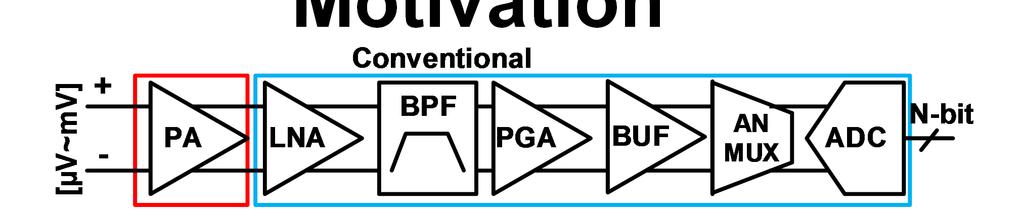


3 Motivation C. Lopez, IEEE TBioCAS,


4 Clinical Applications Alzheimer s disease is 6 th leading cause of death in US Neurodegenerative disease that also effects families of the patients $200B annual cost Need new tools to study causes to find cure 4
5 Schematic Signal Ref TIA BPF OSC f SIG f REF BFADC f= f REF f SIG N=f REF / f DFF Counter Freq. subtractor Neural BFADC Recording system Fully Integrated on-chip enabling high channel count density Digital Time-based Beat Frequency ADC 5
6 Analog Front End Signal Ref TIA BPF OSC f SIG f REF BFADC f= f REF f SIG N=f REF / f DFF Counter Freq. subtractor V DD /2 Thick Ox V out W V DD /2 V in 6
7 Band-pass Filter Signal Ref TIA BPF OSC f SIG f REF BFADC f= f REF f SIG N=f REF / f DFF Counter Freq. subtractor HPF LPF V LPF Thick Ox + NWell Caps Thick Ox V HPF V B V B Measured SNDR, (db) nmLP, 0.8V, 25C Spikes LFPs Fundamental Input Frequency (Hz) 7
8 Current Controlled Oscillator Signal Ref TIA BPF OSC f SIG f REF BFADC f= f REF f SIG N=f REF / f DFF Counter Freq. subtractor nmLP, 1.2V, 25C V IN 3b 2b Frequency, (MHz) Code= Bias, (V) 8
9 Beat Frequency ADC BFADC Signal Ref TIA BPF OSC f SIG f REF f= f REF f SIG N=f REF / f DFF Counter Freq. subtractor 9
10 Silicon Odometer Beat Frequency Ckt Trap S Carrier D A B D Q C DFF VT (a.u.) Trapping Detrapping 10
11 Silicon Odometer Beat Frequency Ckt Trap S Carrier D A D Q C B DFF VT (a.u.) Trapping Detrapping A B 11
12 Silicon Odometer Beat Frequency Ckt Trap S Carrier D A B D Q C DFF VT (a.u.) Trapping Detrapping B A 12
13 Silicon Odometer Beat Frequency Ckt Trap S Carrier D A D Q C B DFF VT (a.u.) Trapping Detrapping B C f C =f A -f B A Sub-ps resolution + sub-µs measurement time 13

14 Beat Frequency ADC BFADC Signal Ref TIA BPF OSC f SIG f REF f= f REF f SIG N=f REF / f DFF Counter freq=f SIG Conventional Counter N Freq. subtractor freq=f REF /N 0 14
15 Linear vs BFADC Transfer Function f=f REF - f SIG freq=f SIG Counter N freq=f SIG DFF Counter N freq=f REF /N 0 freq=f REF N N 0 N= N 0 f SIG f REF N N 0 f SIG N= fsig -f REF f REF f SIG f REF f SIG N Linear Quantizer BF Quantizer (This work) = = = (Table shows quantizer gain normalized to f REF ) 15
16 Bench-top Performance SNR, [db] nmLP, 0.8V, 25C Input Voltage [dbfs] N=34.5 BF Quantizer Gain, [Count/freq] N= f SIG /f REF F in = 416Hz N = 34.5 gain is ~1100 0dBFS = 1.2V 16


17 In-vivo Results Purkinje fibers in anesthetized WT/FVB mouse Tungsten stimulation electrode Glass micropipette recording electrode Flavoprotien Autofluorescence to locate fibers 17
18 Comparison Table Parameters This Work [11]JSSC'17 [12]JSSC'16 [13]CICC'15 [5]CICC'15 [14]TCAS-I'15 ADC Type Beat Freq. VCO CT- VCO- 1-Step BF Incr.- Process/Supply 65nm/0.8V 40nm/1.2V 130nm/1.2V 130nm/1.2v 65nm/1.2V 180nm/1.2V Bandwidth 4.5kHz 200Hz 15MHz 1.7MHz 1.2KHz 4kHz Sampling Rate 50kHz 3kHz 500MHz 250MHz 50kHz 8kHz In 0db [dbfs]* SNDR 1mVpp [db]** ENOB 1mVpp [b]** Power 52uW 7uW 20mW 910uW 34uW 34.8uW F in [pj/conv]*** 900Hz 3Hz 4.15MHz 500kHz 300Hz 175Hz Chip Area [mm 2 ] Area/Ch [mm 2 ] (Relative) (1x) (14.5x) 1.3 (138x) 0.04 (4.3x) (8.3x) (5.9x) Experiment In-vivo In-vitro *Input Amplitude at SNDR=0dB, 0dBFS=1.2V **Reported at V ***FoM =Power/(2*BW*2 ENOB in =1mV pp ) 18

19 Die Photo All passives on-chip mm 2 /channel 0.046mm 2 Total area 19
20 Conclusions Beat Frequency ADC for Intra Electrode Neural Recording proposed Fully integrated- no off-chip passives Low channel area mm dB 1mV pp input In-vivo experiment supports efficacy This research was supported in part by NSF IGERT grant DGE and NIH grant NS
A VCO-Based ADC Employing a Multi- Phase Noise-Shaping Beat Frequency Quantizer for Direct Sampling of Sub-1mV Input Signals
 A VCO-Based ADC Employing a Multi- Phase Noise-Shaping Beat Frequency Quantizer for Direct Sampling of Sub-1mV Input Signals Bongjin Kim, Somnath Kundu, Seokkyun Ko and Chris H. Kim University of Minnesota,
A Multi-phase VCO Quantizer based Adaptive Digital LDO in 65nm CMOS Technology
 A Multi-phase VCO Quantizer based Adaptive Digital LDO in 65nm CMOS Technology Somnath Kundu and Chris H. Kim University of Minnesota Dept. of ECE 1 Presentation Outline Analog vs. digital Low DropOut
A stability-improved single-opamp third-order ΣΔ modulator by using a fully-passive noise-shaping SAR ADC and passive adder
 A stability-improved single-opamp third-order ΣΔ modulator by using a fully-passive noise-shaping SAR ADC and passive adder Zhijie Chen, Masaya Miyahara, and Akira Matsuzawa Tokyo Institute of Technology,
A 0.2-to-1.45GHz Subsampling Fractional-N All-Digital MDLL with Zero-Offset Aperture PD-Based Spur Cancellation and In-Situ Timing Mismatch Detection
 A 0.2-to-1.45GHz Subsampling Fractional-N All-Digital MDLL with Zero-Offset Aperture PD-Based Spur Cancellation and In-Situ Timing Mismatch Detection Somnath Kundu 1, Bongjin Kim 1,2, Chris H. Kim 1 1
A Electrochemical CMOS Biosensor Array with In-Pixel Averaging Using Polar Modulation
 Session 11 - CMOS Biochips and Bioelectronics A 16 20 Electrochemical CMOS Biosensor Array with In-Pixel Averaging Using Polar Modulation Chung-Lun Hsu *, Alexander Sun *, Yunting Zhao *, Eliah Aronoff-Spencer
Silicon Odometer: An On-Chip Reliability Monitor for Measuring Frequency Degradation of Digital Circuits
 Silicon Odometer: An On-Chip Reliability Monitor for Measuring Frequency Degradation of Digital Circuits Tae-Hyoung Kim, Randy Persaud and Chris H. Kim Department of Electrical and Computer Engineering
SiNANO-NEREID Workshop:
 SiNANO-NEREID Workshop: Towards a new NanoElectronics Roadmap for Europe Leuven, September 11 th, 2017 WP3/Task 3.2 Connectivity RF and mmw Design Outline Connectivity, what connectivity? High data rates
RTN Induced Frequency Shift Measurements Using a Ring Oscillator Based Circuit
 RTN Induced Frequency Shift Measurements Using a Ring Oscillator Based Circuit Qianying Tang 1, Xiaofei Wang 1, John Keane 2, and Chris H. Kim 1 1 University of Minnesota, Minneapolis, MN 2 Intel Corporation,
20 GHz Low Power QVCO and De-skew Techniques in 0.13µm Digital CMOS. Masum Hossain & Tony Chan Carusone University of Toronto
 20 GHz Low Power QVCO and De-skew Techniques in 0.13µm Digital CMOS Masum Hossain & Tony Chan Carusone University of Toronto masum@eecg.utoronto.ca Motivation Data Rx3 Rx2 D-FF D-FF Rx1 D-FF Clock Clock
A 9.35-ENOB, 14.8 fj/conv.-step Fully- Passive Noise-Shaping SAR ADC
 A 9.35-ENOB, 14.8 fj/conv.-step Fully- Passive Noise-Shaping SAR ADC Zhijie Chen, Masaya Miyahara, Akira Matsuzawa Tokyo Institute of Technology Symposia on VLSI Technology and Circuits Outline Background
Impact of Interconnect Length on. Degradation
 Impact of Interconnect Length on BTI and HCI Induced Frequency Degradation Xiaofei Wang, Pulkit Jain, Dong Jiao and Chris H. Kim University of Minnesota, Minneapolis, MN xfwang@umn.edu www.umn.edu/~chriskim/
Fast Characterization of PBTI and NBTI Induced Frequency Shifts under a Realistic Recovery Bias Using a Ring Oscillator Based Circuit
 Fast Characterization of PBTI and NBTI Induced Frequency Shifts under a Realistic Recovery Bias Using a Ring Oscillator Based Circuit 1,2 Xiaofei Wang, 1 Seung-hwan Song, 1 Ayan Paul and 1 Chris H. Kim
A Low Phase Noise 24/77 GHz Dual-Band Sub-Sampling PLL for Automotive Radar Applications in 65 nm CMOS Technology
 A Low Phase Noise 24/77 GHz Dual-Band Sub-Sampling PLL for Automotive Radar Applications in 65 nm CMOS Technology Xiang Yi, Chirn Chye Boon, Junyi Sun, Nan Huang and Wei Meng Lim VIRTUS, Nanyang Technological
Proposing. An Interpolated Pipeline ADC
 Proposing An Interpolated Pipeline ADC Akira Matsuzawa Tokyo Institute of Technology, Japan Matsuzawa & Okada Lab. Background 38GHz long range mm-wave system Role of long range mm-wave Current Optical
A Mostly Digital Variable-Rate Continuous- Time ADC Modulator
 A Mostly Digital Variable-Rate Continuous- Time ADC Modulator Gerry Taylor 1,2, Ian Galton 1 1 University of California at San Diego, La Jolla, CA 2 Analog Devices, San Diego, CA INTEGRATED SIGNAL PROCESSING
Architectures and Design Methodologies for Very Low Power and Power Effective A/D Sigma-Delta Converters
 0 Architectures and Design Methodologies for Very Low Power and Power Effective A/D Sigma-Delta Converters F. Maloberti University of Pavia - Italy franco.maloberti@unipv.it 1 Introduction Summary Sigma-Delta
All-Digital PLL Frequency and Phase Noise Degradation Measurements Using Simple On-Chip Monitoring Circuits
 All-Digital PLL Frequency and Noise Degradation Measurements Using Simple On-Chip Monitoring Circuits Gyusung Park, Minsu Kim and Chris H. Kim Department of Electrical and Computer Engineering University
A 12-bit Interpolated Pipeline ADC using Body Voltage Controlled Amplifier
 A 12-bit Interpolated Pipeline ADC using Body Voltage Controlled Amplifier Hyunui Lee, Masaya Miyahara, and Akira Matsuzawa Tokyo Institute of Technology, Japan Outline Background Body voltage controlled
12-bit 50/100/125 MSPS 1-channel ADC
 SPECIFICATION 1 FEATURES TSMC CMOS 65 nm High speed pipelined ADC Resolution 12 bit Conversion rate 50/100/125 MHz Different power supplies for digital (1.2 V) and analog (1.2 V) parts Low standby current
EECS 290C: Advanced circuit design for wireless Class Final Project Due: Thu May/02/2019
 EECS 290C: Advanced circuit design for wireless Class Final Project Due: Thu May/02/2019 Project: A fully integrated 2.4-2.5GHz Bluetooth receiver. The receiver has LNA, RF mixer, baseband complex filter,
An implantable electrical stimulator for phrenic nerve stimulation
 J. Biomedical Science and Engineering, 2012, 5, 141-145 JBiSE http://dx.doi.org/10.4236/jbise.2012.53018 Published Online March 2012 (http://www.scirp.org/journal/jbise/) An implantable electrical stimulator
Cost Effective Spread Spectrum Clock Generator Design Chulwoo Kim, Minyoung Song, Sewook Hwang
 Cost Effective Spread Spectrum Clock Generator Design Chulwoo Kim, Minyoung Song, Sewook Hwang Advanced Integrated Systems Lab. Korea University, Seoul, Korea Outline Introduction Spread Spectrum Clock
5.5: A 3.2 to 4GHz, 0.25µm CMOS Frequency Synthesizer for IEEE a/b/g WLAN
 5.5: A 3.2 to 4GHz, 0.25µm CMOS Frequency Synthesizer for IEEE 802.11a/b/g WLAN Manolis Terrovitis, Michael Mack, Kalwant Singh, and Masoud Zargari 1 Atheros Communications, Sunnyvale, California 1 Atheros
BER-optimal ADC for Serial Links
 BER-optimal ADC for Serial Links Speaker Name: Yingyan Lin Co-authors: Min-Sun Keel, Adam Faust, Aolin Xu, Naresh R. Shanbhag, Elyse Rosenbaum, and Andrew Singer Advisor s name: Naresh R. Shanbhag Affiliation:
A 10Gb/s 10mm On-Chip Serial Link in 65nm CMOS Featuring a Half-Rate Time-Based Decision Feedback Equalizer
 A 10Gb/s 10mm On-Chip Serial Link in 65nm CMOS Featuring a Half-Rate Time-Based Decision Feedback Equalizer Po-Wei Chiu, Somnath Kundu, Qianying Tang, and Chris H. Kim University of Minnesota, Minneapolis,
Scalable and Synthesizable. Analog IPs
 Scalable and Synthesizable Analog IPs Akira Matsuzawa Tokyo Institute of Technology Background and Motivation 1 Issues It becomes more difficult to obtain good analog IPs Insufficient design resources
Signal Integrity Design of TSV-Based 3D IC
 Signal Integrity Design of TSV-Based 3D IC October 24, 21 Joungho Kim at KAIST joungho@ee.kaist.ac.kr http://tera.kaist.ac.kr 1 Contents 1) Driving Forces of TSV based 3D IC 2) Signal Integrity Issues
2008/09 Advances in the mixed signal IC design group
 2008/09 Advances in the mixed signal IC design group Mattias Andersson Mixed-Signal IC Design Department for Electrical and Information Technology Lund University 1 Mixed Signal IC Design Researchers Associate
Development of a 20 GS/s Sampling Chip in 130nm CMOS Technology
 Development of a 20 GS/s Sampling Chip in 130nm CMOS Technology 2009 IEEE Nuclear Science Symposium, Orlando, Florida, October 28 th 2009 Jean-Francois Genat On behalf of Mircea Bogdan 1, Henry J. Frisch
Summary Last Lecture
 EE47 Lecture 5 Pipelined ADCs (continued) How many bits per stage? Algorithmic ADCs utilizing pipeline structure Advanced background calibration techniques Oversampled ADCs Why oversampling? Pulse-count
A Current-Measurement Front-End with 160dB Dynamic Range and 7ppm INL
 A Current-Measurement Front-End with 160dB Dynamic Range and 7ppm INL Chung-Lun Hsu and Drew A. Hall University of California, San Diego, La Jolla, CA, USA International Solid-State Circuits Conference
Research and Development Activities in RF and Analog IC Design. RFIC Building Blocks. Single-Chip Transceiver Systems (I) Howard Luong
 Howard Luong") Research and Development Activities in RF and Analog IC Design Howard Luong Analog Research Laboratory Department of Electrical and Electronic Engineering Hong Kong University of Science and Technology
Research and Development Activities in RF and Analog IC Design Howard Luong Analog Research Laboratory Department of Electrical and Electronic Engineering Hong Kong University of Science and Technology
A 0.55 V 7-bit 160 MS/s Interpolated Pipeline ADC Using Dynamic Amplifiers
 A 0.55 V 7-bit 160 MS/s Interpolated Pipeline ADC Using Dynamic Amplifiers James Lin, Daehwa Paik, Seungjong Lee, Masaya Miyahara, and Akira Matsuzawa Tokyo Institute of Technology, Japan Matsuzawa & Okada
5.4: A 5GHz CMOS Transceiver for IEEE a Wireless LAN
 5.4: A 5GHz CMOS Transceiver for IEEE 802.11a Wireless LAN David Su, Masoud Zargari, Patrick Yue, Shahriar Rabii, David Weber, Brian Kaczynski, Srenik Mehta, Kalwant Singh, Sunetra Mendis, and Bruce Wooley
Workshop ESSCIRC. Low-Power Data Acquisition System For Very Small Signals At Low Frequencies With12-Bit- SAR-ADC. 17. September 2010.
 Workshop ESSCIRC Low-Power Data Acquisition System For Very Small Signals At Low Frequencies With12-Bit- SAR-ADC 17. September 2010 Christof Dohmen Outline System Overview Analog-Front-End Chopper-Amplifier
A 400 MHz 4.5 nw 63.8 dbm Sensitivity Wake-up Receiver Employing an Active Pseudo-Balun Envelope Detector
 A 400 MHz 4.5 nw 63.8 dbm Sensitivity Wake-up Receiver Employing an Active Pseudo-Balun Envelope Detector Po-Han Peter Wang, Haowei Jiang, Li Gao, Pinar Sen, Young-Han Kim, Gabriel M. Rebeiz, Patrick P.
EE M255, BME M260, NS M206:
 EE M255, BME M260, NS M206: NeuroEngineering Lecture Set 6: Neural Recording Prof. Dejan Markovic Agenda Neural Recording EE Model System Components Wireless Tx 6.2 Neural Recording Electrodes sense action
Phase-Locked Loops and Their Applications. Advanced PLL Examples (Part II)
") Short Course On Phase-Locked Loops and Their Applications Day 5, PM Lecture Advanced PLL Examples (Part II) Michael Perrott August 15, 2008 Copyright 2008 by Michael H. Perrott All rights reserved. Outline
Short Course On Phase-Locked Loops and Their Applications Day 5, PM Lecture Advanced PLL Examples (Part II) Michael Perrott August 15, 2008 Copyright 2008 by Michael H. Perrott All rights reserved. Outline
Designing Analog and RF Circuits in Nanoscale CMOS Technologies: Scale the Supply, Reduce the Area and Use Digital Gates.
 Designing Analog and RF Circuits in Nanoscale CMOS Technologies: Scale the Supply, Reduce the Area and Use Digital Gates. Peter Kinget Université Catholique de Louvain (Belgium) On sabbatical from: Columbia
Outline. Motivation. Design Challenges. Design of Mode-Switching VCO. Measurement Results. Conclusion 7/8/14
 Mazhareddin Taghivand, Kamal Aggarwal and Ada Poon Dept. of Electrical Engineering Stanford University Outline Motivation Design Challenges Design of Mode-Switching VCO Measurement Results Conclusion 2
Sigma-Delta ADC Tutorial and Latest Development in 90 nm CMOS for SoC
 Sigma-Delta ADC Tutorial and Latest Development in 90 nm CMOS for SoC Jinseok Koh Wireless Analog Technology Center Texas Instruments Inc. Dallas, TX Outline Fundamentals for ADCs Over-sampling and Noise
EE247 Lecture 22. Figures of merit (FOM) and trends for ADCs How to use/not use FOM. EECS 247 Lecture 22: Data Converters 2004 H. K.
 and trends for ADCs How to use/not use FOM. EECS 247 Lecture 22: Data Converters 2004 H. K.") EE247 Lecture 22 Pipelined ADCs Combining the bits Stage implementation Circuits Noise budgeting Figures of merit (FOM) and trends for ADCs How to use/not use FOM Oversampled ADCs EECS 247 Lecture 22:
EE247 Lecture 22 Pipelined ADCs Combining the bits Stage implementation Circuits Noise budgeting Figures of merit (FOM) and trends for ADCs How to use/not use FOM Oversampled ADCs EECS 247 Lecture 22:
A 130mW 100MS/s Pipelined ADC with 69dB SNDR Enabled by Digital Harmonic Distortion Correction. Andrea Panigada, Ian Galton
 A 130mW 100MS/s Pipelined ADC with 69dB SNDR Enabled by Digital Harmonic Distortion Correction Andrea Panigada, Ian Galton University of California at San Diego, La Jolla, CA INTEGRATED SIGNAL PROCESSING
A/D Conversion and Filtering for Ultra Low Power Radios. Dejan Radjen Yasser Sherazi. Advanced Digital IC Design. Contents. Why is this important?
 1 Advanced Digital IC Design A/D Conversion and Filtering for Ultra Low Power Radios Dejan Radjen Yasser Sherazi Contents A/D Conversion A/D Converters Introduction ΔΣ modulator for Ultra Low Power Radios
Tutorial: Quartz Crystal Oscillators & Phase- Locked Loops
 Tutorial: Quartz Crystal Oscillators & Phase- Locked Loops Greg Armstrong (IDT) Dominik Schneuwly (Oscilloquartz) June 13th, 2016 1 Content 1. Quartz Crystal Oscillator (XO) Technology Quartz Crystal Overview
DESIGN OF LOW POWER VCO ENABLED QUANTIZER IN CONTINUOUS TIME SIGMA DELTA ADC FOR SIGNAL PROCESSING APPLICATION
 ISSN: 2395-1680 (ONLINE) DOI: 10.21917/ijme.2016.0033 ICTACT JOURNAL ON MICROELECTRONICS, APRIL 2016, VOLUME: 02, ISSUE: 01 DESIGN OF LOW POWER VCO ENABLED QUANTIZER IN CONTINUOUS TIME SIGMA DELTA ADC
2011/12 Cellular IC design RF, Analog, Mixed-Mode
 2011/12 Cellular IC design RF, Analog, Mixed-Mode Mohammed Abdulaziz, Mattias Andersson, Jonas Lindstrand, Xiaodong Liu, Anders Nejdel Ping Lu, Luca Fanori Martin Anderson, Lars Sundström, Pietro Andreani
CMOS Analog to Digital Converters : State-of-the-Art and Perspectives in Digital Communications ADC
 CMOS Analog to Digital Converters : State-of-the-Art and Perspectives in Digital Communications ADC Hussein Fakhoury and Hervé Petit C²S Research Group Presentation Outline Introduction Basic concepts
A Dual-Step-Mixing ILFD using a Direct Injection Technique for High- Order Division Ratios in 60GHz Applications
 A Dual-Step-Mixing ILFD using a Direct Injection Technique for High- Order Division Ratios in 60GHz Applications Teerachot Siriburanon, Wei Deng, Ahmed Musa, Kenichi Okada, and Akira Matsuzawa Tokyo Institute
A VCO-based analog-to-digital converter with secondorder sigma-delta noise shaping
 A VCO-based analog-to-digital converter with secondorder sigma-delta noise shaping The MIT Faculty has made this article openly available. Please share how this access benefits you. Your story matters.
A 3.9 ns 8.9 mw 4 4 Silicon Photonic Switch Hybrid-Integrated with CMOS Driver
 A 3.9 ns 8.9 mw 4 4 Silicon Photonic Switch Hybrid-Integrated with CMOS Driver A. Rylyakov, C. Schow, B. Lee, W. Green, J. Van Campenhout, M. Yang, F. Doany, S. Assefa, C. Jahnes, J. Kash, Y. Vlasov IBM
A 1.7-to-2.2GHz Full-Duplex Transceiver System with >50dB Self-Interference Cancellation over 42MHz Bandwidth
 A 1.7-to-2.2GHz Full-Duplex Transceiver System with >50dB Self-Interference Cancellation Tong Zhang, Ali Najafi, Chenxin Su, Jacques C. Rudell University of Washington, Seattle Feb. 8, 2017 International
Converter IC for Cellular Phone. Mode Digitally-Controlled Buck. A 4 µa-quiescent-current Dual- Applications. Jianhui Zhang Prof.
 A 4 µa-quiescent-current Dual- Mode Digitally-Controlled Buck Converter IC for Cellular Phone Applications Jinwen Xiao Angel Peterchev Jianhui Zhang Prof. Seth Sanders Power Electronics Group Dept. of
Digital PWM IC Control Technology and Issues
 Digital PWM IC Control Technology and Issues Prof. Seth R. Sanders Angel V. Peterchev Jinwen Xiao Jianhui Zhang Department of EECS University of California, Berkeley Digital Control Advantages implement
High Performance Digital Fractional-N Frequency Synthesizers
 High Performance Digital Fractional-N Frequency Synthesizers Michael Perrott October 16, 2008 Copyright 2008 by Michael H. Perrott All rights reserved. Why Are Digital Phase-Locked Loops Interesting? PLLs
Duty-Cycle Shift under Asymmetric BTI Aging: A Simple Characterization Method and its Application to SRAM Timing
 Duty-Cycle Shift under Asymmetric BTI Aging: A Simple Characterization Method and its Application to SRAM Timing 1 Xiaofei Wang, 2 John Keane, 2 Pulkit Jain, 3 Vijay Reddy and 1 Chris H. Kim 1 University
Challenges in Designing CMOS Wireless System-on-a-chip
 Challenges in Designing CMOS Wireless System-on-a-chip David Su Atheros Communications Santa Clara, California IEEE Fort Collins, March 2008 Introduction Outline Analog/RF: CMOS Transceiver Building Blocks
An RF-Powered Temperature Sensor Designed for Biomedical Applications
 An RF-Powered Temperature Sensor Designed for Biomedical Applications Gustavo Campos Martins, Fernando Rangel de Sousa GRF, UFSC September 4, 2013 Gustavo C. Martins (GRF, UFSC) RF-Powered Temperature
EE247 Lecture 23. Advanced calibration techniques. Compensating inter-stage amplifier non-linearity Calibration via parallel & slow ADC
 EE247 Lecture 23 Pipelined ADCs Combining the bits Stage implementation Circuits Noise budgeting Advanced calibration techniques Compensating inter-stage amplifier non-linearity Calibration via parallel
ECEN620: Network Theory Broadband Circuit Design Fall 2014
 ECEN60: Network Theory Broadband Circuit Design Fall 014 Lecture 13: Frequency Synthesizer Examples Sam Palermo Analog & Mixed-Signal Center Texas A&M University Agenda Frequency Synthesizer Examples Design
SG2525A SG3525A REGULATING PULSE WIDTH MODULATORS
 SG2525A SG3525A REGULATING PULSE WIDTH MODULATORS 8 TO 35 V OPERATION 5.1 V REFERENCE TRIMMED TO ± 1 % 100 Hz TO 500 KHz OSCILLATOR RANGE SEPARATE OSCILLATOR SYNC TERMINAL ADJUSTABLE DEADTIME CONTROL INTERNAL
FUNDAMENTALS OF ANALOG TO DIGITAL CONVERTERS: PART I.1
 FUNDAMENTALS OF ANALOG TO DIGITAL CONVERTERS: PART I.1 Many of these slides were provided by Dr. Sebastian Hoyos January 2019 Texas A&M University 1 Spring, 2019 Outline Fundamentals of Analog-to-Digital
A single-slope 80MS/s ADC using two-step time-to-digital conversion
 A single-slope 80MS/s ADC using two-step time-to-digital conversion The MIT Faculty has made this article openly available. Please share how this access benefits you. Your story matters. Citation As Published
A 20GHz Class-C VCO Using Noise Sensitivity Mitigation Technique
 Matsuzawa Lab. Matsuzawa & Okada Lab. Tokyo Institute of Technology A 20GHz Class-C VCO Using Noise Sensitivity Mitigation Technique Kento Kimura, Kenichi Okada and Akira Matsuzawa (WE2C-2) Matsuzawa &
Comparison between Analog and Digital Current To PWM Converter for Optical Readout Systems
 Comparison between Analog and Digital Current To PWM Converter for Optical Readout Systems 1 Eun-Jung Yoon, 2 Kangyeob Park, 3* Won-Seok Oh 1, 2, 3 SoC Platform Research Center, Korea Electronics Technology
Design and Implementation of High-Speed CMOS Clock and Data Recovery Circuit for Optical Interconnection Applications. Seong-Jun Song. Dec.
 MS Thesis esign and Implementation of High-Speed CMOS Clock and ata Recovery Circuit for Optical Interconnection Applications Seong-Jun Song ec. 20, 2002 oratory, epartment of Electrical Engineering and
Insights Into Circuits for Frequency Synthesis at mm-waves Andrea Mazzanti Università di Pavia, Italy
 RFIC2014, Tampa Bay June 1-3, 2014 Insights Into Circuits for Frequency Synthesis at mm-waves Andrea Mazzanti Università di Pavia, Italy High data rate wireless networks MAN / LAN PAN ~7GHz of unlicensed
A Sub-0.75 RMS-Phase-Error Differentially-Tuned Fractional-N Synthesizer with On-Chip LDO Regulator and Analog-Enhanced AFC Technique
 A Sub-0.75 RMS-Phase-Error Differentially-Tuned Fractional-N Synthesizer with On-Chip LDO Regulator and Analog-Enhanced AFC Technique Lei Lu, Lingbu Meng, Liang Zou, Hao Min and Zhangwen Tang Fudan University,
System-Level Time-Domain Behavioral Modeling for A Mobile WiMax Transceiver
 System-Level Time-Domain Behavioral Modeling for A Mobile WiMax Transceiver Jie He, Jun Seo Yang, Yongsup Kim, and Austin S. Kim HIDS Lab, Telecommunication R&D Center, Samsung Electronics jie.he@samung.com,
A Low Power 900MHz Superheterodyne Compressive Sensing Receiver for Sparse Frequency Signal Detection
 A Low Power 900MHz Superheterodyne Compressive Sensing Receiver for Sparse Frequency Signal Detection Hamid Nejati and Mahmood Barangi 4/14/2010 Outline Introduction System level block diagram Compressive
A 60GHz Sub-Sampling PLL Using A Dual-Step-Mixing ILFD
 A 60GHz Sub-Sampling PLL Using A Dual-Step-Mixing ILFD Teerachot Siriburanon, Tomohiro Ueno, Kento Kimura, Satoshi Kondo, Wei Deng, Kenichi Okada, and Akira Matsuzawa Tokyo Institute of Technology, Japan
A DRY ELECTRODE LOW POWER CMOS EEG ACQUISITION SOC FOR SEIZURE DETECTION
 A DRY ELECTRODE LOW POWER CMOS EEG ACQUISITION SOC FOR SEIZURE DETECTION TEAM 6: MATTHIEU DURBEC, VALENTIN BERANGER, KARIM ELOUELDRHIRI ECE 6414 SPRING 2017 OUTLINE Project motivation Design overview Body-Electrode
A Low-power Area-efficient Switching Scheme for Chargesharing
 A Low-power Area-efficient Switching Scheme for Chargesharing DACs in SAR ADCs The MIT Faculty has made this article openly available. Please share how this access benefits you. Your story matters. Citation
V d = "1" if V in > V m. Fig 2: Frequency analysis of the PDM signal. Fig 1: PDM signal generation
 A low voltage CMOS Pulse Duration Modulator Meena Ramani,Ashok Verma, Dr. John G Harris Dept. of Electrical & Computer Engineering University of Florida, Gainesville, FL 32611, USA Email: meena@cnel.ufl.edu,
A 25MS/s 14b 200mW Σ Modulator in 0.18µm CMOS
 UT Mixed-Signal/RF Integrated Circuits Seminar Series A 25MS/s 14b 200mW Σ Modulator in 0.18µm CMOS Pio Balmelli April 19 th, Austin TX 2 Outline VDSL specifications Σ A/D converter features Broadband
A CMOS Frequency Synthesizer with an Injection-Locked Frequency Divider for a 5 GHz Wireless LAN Receiver. Hamid Rategh
 A CMOS Frequency Synthesizer with an Injection-Locked Frequency Divider for a 5 GHz Wireless LAN Receiver Hamid Rategh Center for Integrated Systems Stanford University OUTLINE Motivation Introduction
A 6-bit Subranging ADC using Single CDAC Interpolation
 A 6-bit Subranging ADC using Single CDAC Interpolation Hyunui Lee, Masaya Miyahara, and Akira Matsuzawa Tokyo Institute of Technology, Japan Outline Background Interpolation techniques 6-bit, 500 MS/s
Frequency Synthesizers
 Phase-Locked Loops Frequency Synthesizers Ching-Yuan Yang National Chung-Hsing University epartment of Electrical Engineering One-port oscillators ecaying impulse response of a tank Adding of negative
Low-Power Pipelined ADC Design for Wireless LANs
 Low-Power Pipelined ADC Design for Wireless LANs J. Arias, D. Bisbal, J. San Pablo, L. Quintanilla, L. Enriquez, J. Vicente, J. Barbolla Dept. de Electricidad y Electrónica, E.T.S.I. de Telecomunicación,
Gert Veale / Christo Nel Grintek Ewation
 Phase noise in RF synthesizers Gert Veale / Christo Nel Grintek Ewation Introduction & Overview Where are RF synthesizers used? What is phase noise? Phase noise eects Classic RF synthesizer architecture
Radio-Frequency Conversion and Synthesis (for a 115mW GPS Receiver)
") Radio-Frequency Conversion and Synthesis (for a 115mW GPS Receiver) Arvin Shahani Stanford University Overview GPS Overview Frequency Conversion Frequency Synthesis Conclusion GPS Overview: Signal Structure
Radio-Frequency Conversion and Synthesis (for a 115mW GPS Receiver) Arvin Shahani Stanford University Overview GPS Overview Frequency Conversion Frequency Synthesis Conclusion GPS Overview: Signal Structure
Design of Continuous Time Sigma Delta ADC for Signal Processing Application
 International Journal of Luminescence and Applications (ISSN: 22776362) Vol. 7, No. 34, October December 2017. Article ID: 254. pp.486490. Design of Continuous Time Sigma Delta ADC for Signal Processing
Research Overview. Payam Heydari Nanoscale Communication IC Lab University of California, Irvine, CA
 Research Overview Payam Heydari Nanoscale Communication IC Lab University of California, Irvine, CA NCIC Lab (Sub)-MMW measurement facility for frequencies up to 120GHz Students 11 Ph.D. students and 2
26.8: A 1.9GHz Single-Chip CMOS PHS Cellphone
 26.8: A 1.9GHz Single-Chip CMOS PHS Cellphone William W. Si, Srenik Mehta, Hirad Samavati, Manolis Terrovitis, Michael Mack, KeithOnodera, SteveJen, Susan Luschas, Justin Hwang, SuniMendis, DavidSu, BruceWooley
Digital-Centric RF-CMOS technology
 1 Digital-Centric RF-CMOS technology Akira Department of Physical Electronics Tokyo Institute of Technology Contents 2 Digital-centric CMOS tuner technology Conventional AM/FM tuner Analog-centric CMOS
AST-GLSRF GLONASS Downconverter
 AST-GLSRF GLONASS Downconverter Document History Sl No. Version Changed By Changed On Change Description 1 0.1 Sudhir N S 17-Nov-2014 Created Contents Features Applications General Description Functional
A Complete Analog Front-End IC Design for ECG Signal Acquisition
 A Complete Analog Front-End IC Design for ECG Signal Acquisition Yang Xu, Yanling Wu, Xiaotong Jia School of Electrical and Computer Engineering Georgia Institute of Technology yxu327@gatech.edu, yanlingwu@gatech.edu,
How to turn an ADC into a DAC: A 110dB THD, 18mW DAC using sampling of the output and feedback to reduce distortion
 How to turn an ADC into a DAC: A 110dB THD, 18mW DAC using sampling of the output and feedback to reduce distortion Axel Thomsen, Design Manager Silicon Laboratories Inc. Austin, TX 1 Why this talk? A
Digitally Assisted Radio Evolution DARE
 Digitally Assisted Radio Evolution DARE Pietro Andreani Department of Electrical and Information Technology Lund University, Sweden The DARE Concept Focus on 4G radio receiver and frequency generation
A 60-dB Image Rejection Filter Using Δ-Σ Modulation and Frequency Shifting
 A 60-dB Image Rejection Filter Using Δ-Σ Modulation and Frequency Shifting Toshihiro Konishi, Koh Tsuruda, Shintaro Izumi, Hyeokjong Lee, Hidehiro Fujiwara, Takashi Takeuchi, Hiroshi Kawaguchi, and Masahiko
A 4 µa-quiescent-current Dual- Mode Digitally-Controlled Buck Converter IC for Cellular Phone Applications
 A 4 µa-quiescent-current Dual- Mode Digitally-Controlled Buck Converter IC for Cellular Phone Applications Jinwen Xiao Angel Peterchev Jianhui Zhang Prof. Seth Sanders Power Electronics Group Dept. of
Pankaj Naik Electronic and Instrumentation Deptt. SGSITS, Indore, India. Priyanka Sharma Electronic and. SGSITS, Indore, India
 Designing Of Current Mode Instrumentation Amplifier For Bio-Signal Using 180nm CMOS Technology Sonu Mourya Electronic and Instrumentation Deptt. SGSITS, Indore, India Pankaj Naik Electronic and Instrumentation
12-Bit 1-channel 4 MSPS ADC
 SPECIFICATION 1 FEATURES 12-Bit 1-channel 4 MSPS ADC TSMC CMOS 65 nm Resolution 12 bit Single power supplies for digital and analog parts (2.5 V) Sampling rate up to 4 MSPS Standby mode (current consumption
Fundamentals of Data Converters. DAVID KRESS Director of Technical Marketing
 Fundamentals of Data Converters DAVID KRESS Director of Technical Marketing 9/14/2016 Analog to Electronic Signal Processing Sensor (INPUT) Amp Converter Digital Processor Actuator (OUTPUT) Amp Converter
A 2.5 V 109 db DR ADC for Audio Application
 276 JOURNAL OF SEMICONDUCTOR TECHNOLOGY AND SCIENCE, VOL.10, NO.4, DECEMBER, 2010 A 2.5 V 109 db DR ADC for Audio Application Gwangyol Noh and Gil-Cho Ahn Abstract A 2.5 V feed-forward second-order deltasigma
A GSM Band Low-Power LNA 1. LNA Schematic
 A GSM Band Low-Power LNA 1. LNA Schematic Fig1.1 Schematic of the Designed LNA 2. Design Summary Specification Required Simulation Results Peak S21 (Gain) > 10dB >11 db 3dB Bandwidth > 200MHz (
A 0.7 V-to-1.0 V 10.1 dbm-to-13.2 dbm 60-GHz Power Amplifier Using Digitally- Assisted LDO Considering HCI Issues
 A 0.7 V-to-1.0 V 10.1 dbm-to-13.2 dbm 60-GHz Power Amplifier Using Digitally- Assisted LDO Considering HCI Issues Rui Wu, Yuuki Tsukui, Ryo Minami, Kenichi Okada, and Akira Matsuzawa Tokyo Institute of
D f ref. Low V dd (~ 1.8V) f in = D f ref
 f in = D f ref") A 5.3 GHz Programmable Divider for HiPerLAN in 0.25µm CMOS N. Krishnapura 1 & P. Kinget 2 Lucent Technologies, Bell Laboratories, USA. 1 Currently at Columbia University, New York, NY, 10027, USA. 2 Currently
A 5.3 GHz Programmable Divider for HiPerLAN in 0.25µm CMOS N. Krishnapura 1 & P. Kinget 2 Lucent Technologies, Bell Laboratories, USA. 1 Currently at Columbia University, New York, NY, 10027, USA. 2 Currently
Re-configurable Switched Capacitor Sigma-Delta Modulator for MEMS Microphones in Mobiles
 Re-configurable Switched Capacitor Sigma-Delta Modulator for MEMS Microphones in Mobiles M. Grassi, F. Conso, G. Rocca, P. Malcovati and A. Baschirotto Abstract This paper presents a reconfigurable discrete-time
A 1.9GHz Single-Chip CMOS PHS Cellphone
 A 1.9GHz Single-Chip CMOS PHS Cellphone IEEE JSSC, Vol. 41, No.12, December 2006 William Si, Srenik Mehta, Hirad Samavati, Manolis Terrovitis, Michael Mack, Keith Onodera, Steve Jen, Susan Luschas, Justin