A 10Gb/s 10mm On-Chip Serial Link in 65nm CMOS Featuring a Half-Rate Time-Based Decision Feedback Equalizer
|
|
|
- Edmund Lang
- 6 years ago
- Views:
Transcription
1 A 10Gb/s 10mm On-Chip Serial Link in 65nm CMOS Featuring a Half-Rate Time-Based Decision Feedback Equalizer Po-Wei Chiu, Somnath Kundu, Qianying Tang, and Chris H. Kim University of Minnesota, Minneapolis, MN chiux148@umn.edu Symposia on VLSI Technology and Circuits
2 Outline Background Proposed Time-Based Decision Feedback Equalizer (DFE) 65nm Test Chip Details BER Measurements Conclusion Slide 1

3 On-Chip Interconnect Scaling Interconnect length not scaling down at same rate as transistor scaling Interconnect power larger fraction of total chip power Slide 2


4 Interconnect Design Challenges A 2cm x 2cm processor requires interconnect lengths as long as 15 mm Signal loss due to RC parasitics limits performance Slide 3
5 Standard Solution: Repeater n-1 n Latency (ns) Repeater (no equalization) Equalizer n=1 n=2 n=3 n= Length (mm) [2] L. Zhang, et al., TVLSI, Pros: Improved RC delay, digital implementation, good CAD tool support Cons: Floorplan disruption, increased power consumption Slide 4
6 TX/RX Equalization Techniques TX FFE Channel RX CTLE + DFE Volt. Gain Volt. Time Freq. Time Feed Forward Equalizer (FFE) Continuous Time Linear Equalizer (CTLE) Decision Feedback Equalizer (DFE) Slide 5
7 Equalization Techniques for On- Chip Interconnects INP V DD OUTN Active Inductor V OUT V SS V DD INN OUTP D+ D- Dd- Dd+ V SS I DRV I PE [3] D. Walter, et al., ISSCC, [4] S. Lee, et al., ISSCC, Left: Utilizes capacitors to pre-distort signal Right: Utilizes current mode logic to pre-distort signal, inductor provides frequency peaking Slide 6
8 Conventional DFE Implementation V RX (t) Σ V DFE Slicer x[n] Output W N... W 2 W 1 Z Z -1 Z -1 I BIAS W 1 W 2 W N Current mode logic... Slide 7
9 Proposed Time-Based DFE V RX (t) Σ t PD PD=Phase Detector x[n] Output W N... W 2 W 1 Z Z -1 Z -1 CLK W N W 2 W 1 t Delay line Slide 8
10 DFE Comparison CLK PD Pros Cons Conventional DFE Ultra high speed (>20Gb/s) Analog intensive, headroom issues, limited number of taps, large power consumption Time-based DFE Inverter based, scalable to large number of taps, low power consumption Moderate speed Slide 9
11 Time-Based DFE Operation Input V RX (t) N REF w/o DFE N DFE w/ DFE W 1 W 2 W 1 W 2 W 1 W 2 W 1 Decision Results Slide 10
12 Time-Based DFE Operation Input V RX (t) w/o DFE D=1 D=0 w/ DFE Slide 11
13 Optimizing Time-Based DFE T 1 T 2 T 3 x[n] PD Output T REF T REF T REF Slide 12
14 Optimizing Time-Based DFE x[n] T 1 T 2 PD Output T REF 2T REF -T 3 Performs same time-based comparison with fewer delay stages low power consumption All delay stages are identical Slide 13
15 Delay Stage Implementation Analog Control Digital Control T RX T W1X1 PD T REF T -W2X2 V RX (t) Σ t PD x[n] Output W 2 W 1 Z -1 Z -1 Slide 14
16 Delay Stage w/ Analog Control V RX nm GP CMOS, 25 C 4X V RX 2X V RX 1X V RX V RX V RX Delay (ps) X 4X 1X 2X 4X V RX (V) Delay controlled by analog signal Slide 15
17 Delay Stage w/ Digital Control D w<5> 8 65nm GP CMOS, 25 C 4X D w<4> 2X D w<3> 1X 1X 2X 4X Delay (ps) D=0 D=1 4X 4X D w<2> D w<1> D w<0> w<5:0> Inverters for coarse control, capacitors for fine control Capacitor connected to VDD for wider delay range Slide 16
18 65nm Test Chip Diagram TX: Half rate (i.e. F clk =5GHz for 10 Gbps) FFE RX: Transimpedance amp.(tia), time-based DFE Testing features: 15 bit PRBS, in-situ eye-diagram monitor Slide 17
19 Time-Based DFE Implementation -W 2 1X 2X4X 8X TIA CLK (5GHz) T REF T RX T -W2X2 T o D[n] T PD FF FF W1X1 T o + T Zero-offset aperture PD D Q V RX (t) W 1 T o + T W 1 RST CLK (5GHz) T RX T REF T W1X1 T -W2X2 T o PD D[n+1] FF FF Transmission gate resistor for impedance matching Half rate operation Zero-offset aperture phase detector (PD) -W 2 Slide 18
![Eye-Diagram Measurement [4] S. Lee, et al., ISSCC, 2013.](/docs-images/74/70227840/images/20-0.jpg "Typical BER eye diagram Y-axis: Voltage offset X-axis: Unit")
20 Eye-Diagram Measurement [4] S. Lee, et al., ISSCC, Typical BER eye diagram Y-axis: Voltage offset X-axis: Unit Interval Slide 19
![Eye-Diagram Measurement [4] S. Lee, et al., ISSCC, 2013.](/docs-images/74/70227840/images/21-0.jpg "Typical BER eye diagram Y-axis: Voltage offset X-axis: Unit Interval TB-DFE BER eye diagram Y-axis:")
21 Eye-Diagram Measurement [4] S. Lee, et al., ISSCC, Typical BER eye diagram Y-axis: Voltage offset X-axis: Unit Interval TB-DFE BER eye diagram Y-axis: Time offset X-axis: Unit Interval Slide 20
22 In-situ BER Eye-Diagram T Monitor UI CLK Phase Delay T REF DFE T RX DFE T PD D' D BER Monitor Err 11b Counter Parallel to serial Error count PRBS 6-bit programmable delay to sweep the X,Y-axes BER monitor compares TX data with RX data Slide 21


23 Measured BER Eye Diagram Y-axis is time offset, not voltage offset Slide 22
24 Measured BER Bathtub 65nm GP, 1.2V, 25ºC Bit Error Rate UI Phase (UI) w/o DFE w/ DFE 1.2 Eye width=0.43 BER=10-12 with DFE Slide 23


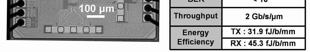
25 Die Photo and Feature Summary Slide 24
26 Performance Comparison ISSCC'09 [5] ISSCC'12 [6] ISSCC'13 [7] VLSI'15 [8] Technology 90nm 65nm 65nm 65nm TX and RX Current mode Voltage mode Current mode CTLE-based driver+tia driver+sense amp. driver+sense amp. repeater Features No DFE No DFE No DFE No DFE This work 65nm Voltage mode driver+tia 2-tap TB-DFE Data Rate 4Gb/s 10Gb/s 3Gb/s 4Gb/s 10Gb/s Throughput (Gb/s/µm) Link Length 10mm 6mm 10mm 2.5mm+2.5mm 10mm BER Bathtub < 10E-6 < 10E-12 < 10E-12 < 10E-12 < 10E-12 BER Eye Yes (< 10E-6) No Yes (< 10E-12) No Yes (< 10E-11) Energy TIA 14.4 Efficiency DFE 30.9 (fj/b/mm) FFE 31.9 [5] B. Kim, et al., ISSCC, [6] D. Walter, et al., ISSCC, [7] S. Lee, et al., ISSCC, [8] M. Chen et al., VLSI, Slide 25
27 Conclusion A 10mm, 10 Gbps on-chip serial link implemented in 65nm GP An all-digital inverter based 2-tap half-rate time-based DFE In-situ BER eye diagram monitor Slide 26
To learn fundamentals of high speed I/O link equalization techniques.
 1 ECEN 720 High-Speed Links: Circuits and Systems Lab5 Equalization Circuits Objective To learn fundamentals of high speed I/O link equalization techniques. Introduction An ideal cable could propagate
A 0.2-to-1.45GHz Subsampling Fractional-N All-Digital MDLL with Zero-Offset Aperture PD-Based Spur Cancellation and In-Situ Timing Mismatch Detection
 A 0.2-to-1.45GHz Subsampling Fractional-N All-Digital MDLL with Zero-Offset Aperture PD-Based Spur Cancellation and In-Situ Timing Mismatch Detection Somnath Kundu 1, Bongjin Kim 1,2, Chris H. Kim 1 1
ECEN689: Special Topics in High-Speed Links Circuits and Systems Spring 2012
 ECEN689: Special Topics in High-Speed Links Circuits and Systems Spring 0 Lecture 8: RX FIR, CTLE, & DFE Equalization Sam Palermo Analog & Mixed-Signal Center Texas A&M University Announcements Exam is
A VCO-Based ADC Employing a Multi- Phase Noise-Shaping Beat Frequency Quantizer for Direct Sampling of Sub-1mV Input Signals
 A VCO-Based ADC Employing a Multi- Phase Noise-Shaping Beat Frequency Quantizer for Direct Sampling of Sub-1mV Input Signals Bongjin Kim, Somnath Kundu, Seokkyun Ko and Chris H. Kim University of Minnesota,
Sense Amplifier Comparator with Offset Correction for Decision Feedback Equalization based Receivers
 arxiv:1702.01067v1 [cs.ar] 3 Feb 2017 Sense Amplifier Comparator with Offset Correction for Decision Feedback Equalization based Receivers Naveen Kadayinti, and Dinesh Sharma Department of Electrical Engineering,
A 12-bit Interpolated Pipeline ADC using Body Voltage Controlled Amplifier
 A 12-bit Interpolated Pipeline ADC using Body Voltage Controlled Amplifier Hyunui Lee, Masaya Miyahara, and Akira Matsuzawa Tokyo Institute of Technology, Japan Outline Background Body voltage controlled
A 0.55 V 7-bit 160 MS/s Interpolated Pipeline ADC Using Dynamic Amplifiers
 A 0.55 V 7-bit 160 MS/s Interpolated Pipeline ADC Using Dynamic Amplifiers James Lin, Daehwa Paik, Seungjong Lee, Masaya Miyahara, and Akira Matsuzawa Tokyo Institute of Technology, Japan Matsuzawa & Okada
RTN Induced Frequency Shift Measurements Using a Ring Oscillator Based Circuit
 RTN Induced Frequency Shift Measurements Using a Ring Oscillator Based Circuit Qianying Tang 1, Xiaofei Wang 1, John Keane 2, and Chris H. Kim 1 1 University of Minnesota, Minneapolis, MN 2 Intel Corporation,
A Complete 64Gb/s/lane Active Electrical Repeater. Yue Lu, Jaeduk Han, Nicholas Sutardja Prof. Elad Alon January 23, 2014
 A Complete 64Gb/s/lane Active Electrical Repeater Yue Lu, Jaeduk Han, Nicholas Sutardja Prof. Elad Alon January 23, 2014 The Electrical Signaling Challenge Required I/O speed rising dramatically, but power
A 15.5 db, Wide Signal Swing, Dynamic Amplifier Using a Common- Mode Voltage Detection Technique
 A 15.5 db, Wide Signal Swing, Dynamic Amplifier Using a Common- Mode Voltage Detection Technique James Lin, Masaya Miyahara and Akira Matsuzawa Tokyo Institute of Technology, Japan Matsuzawa & Okada Laḃ
A 5-Gb/s 156-mW Transceiver with FFE/Analog Equalizer in 90-nm CMOS Technology Wang Xinghua a, Wang Zhengchen b, Gui Xiaoyan c,
 4th International Conference on Computer, Mechatronics, Control and Electronic Engineering (ICCMCEE 2015) A 5-Gb/s 156-mW Transceiver with FFE/Analog Equalizer in 90-nm CMOS Technology Wang Xinghua a,
ECEN720: High-Speed Links Circuits and Systems Spring 2017
 ECEN720: High-Speed Links Circuits and Systems Spring 207 Lecture 8: RX FIR, CTLE, DFE, & Adaptive Eq. Sam Palermo Analog & Mixed-Signal Center Texas A&M University Announcements Lab 4 Report and Prelab
A10-Gb/slow-power adaptive continuous-time linear equalizer using asynchronous under-sampling histogram
 LETTER IEICE Electronics Express, Vol.10, No.4, 1 8 A10-Gb/slow-power adaptive continuous-time linear equalizer using asynchronous under-sampling histogram Wang-Soo Kim and Woo-Young Choi a) Department
University of Minnesota, Minneapolis, MN 2. Intel Corporation, Hillsboro, OR 3. Los Alamos National Laboratory, Los Alamos, NM
 Statistical Characterization of Radiation- Induced Pulse Waveforms and Flip-Flop Soft Errors in 14nm Tri-Gate CMOS Using a Back- Sampling Chain (BSC) Technique Saurabh Kumar 1, M. Cho 2, L. Everson 1,
ISSCC 2003 / SESSION 20 / WIRELESS LOCAL AREA NETWORKING / PAPER 20.5
 ISSCC 2003 / SESSION 20 / WIRELESS LOCAL AREA NETWORKING / PAPER 20.5 20.5 A 2.4GHz CMOS Transceiver and Baseband Processor Chipset for 802.11b Wireless LAN Application George Chien, Weishi Feng, Yungping
Comparison between Analog and Digital Current To PWM Converter for Optical Readout Systems
 Comparison between Analog and Digital Current To PWM Converter for Optical Readout Systems 1 Eun-Jung Yoon, 2 Kangyeob Park, 3* Won-Seok Oh 1, 2, 3 SoC Platform Research Center, Korea Electronics Technology
A Multi-phase VCO Quantizer based Adaptive Digital LDO in 65nm CMOS Technology
 A Multi-phase VCO Quantizer based Adaptive Digital LDO in 65nm CMOS Technology Somnath Kundu and Chris H. Kim University of Minnesota Dept. of ECE 1 Presentation Outline Analog vs. digital Low DropOut
Ultra-high-speed Interconnect Technology for Processor Communication
 Ultra-high-speed Interconnect Technology for Processor Communication Yoshiyasu Doi Samir Parikh Yuki Ogata Yoichi Koyanagi In order to improve the performance of storage systems and servers that make up
5.5: A 3.2 to 4GHz, 0.25µm CMOS Frequency Synthesizer for IEEE a/b/g WLAN
 5.5: A 3.2 to 4GHz, 0.25µm CMOS Frequency Synthesizer for IEEE 802.11a/b/g WLAN Manolis Terrovitis, Michael Mack, Kalwant Singh, and Masoud Zargari 1 Atheros Communications, Sunnyvale, California 1 Atheros
A 400 MHz 4.5 nw 63.8 dbm Sensitivity Wake-up Receiver Employing an Active Pseudo-Balun Envelope Detector
 A 400 MHz 4.5 nw 63.8 dbm Sensitivity Wake-up Receiver Employing an Active Pseudo-Balun Envelope Detector Po-Han Peter Wang, Haowei Jiang, Li Gao, Pinar Sen, Young-Han Kim, Gabriel M. Rebeiz, Patrick P.
To learn statistical bit-error-rate (BER) simulation, BER link noise budgeting and using ADS to model high speed I/O link circuits
 simulation, BER link noise budgeting and using ADS to model high speed I/O link circuits") 1 ECEN 720 High-Speed Links: Circuits and Systems Lab6 Link Modeling with ADS Objective To learn statistical bit-error-rate (BER) simulation, BER link noise budgeting and using ADS to model high speed
1 ECEN 720 High-Speed Links: Circuits and Systems Lab6 Link Modeling with ADS Objective To learn statistical bit-error-rate (BER) simulation, BER link noise budgeting and using ADS to model high speed
A Pin and Power Efficient Low Latency 8-12Gb/s/wire 8b8w- Coded SerDes Link for High Loss Channels in 40nm Technology
 A Pin and Power Efficient Low Latency 8-12Gb/s/wire 8b8w- Coded SerDes Link for High Loss Channels in 40nm Technology Anant Singh 1, Dario Carnelli 1, Altay Falay 1, Klaas Hofstra 1, Fabio Licciardello
ECEN 720 High-Speed Links Circuits and Systems
 1 ECEN 720 High-Speed Links Circuits and Systems Lab4 Receiver Circuits Objective To learn fundamentals of receiver circuits. Introduction Receivers are used to recover the data stream transmitted by transmitters.
ECEN 620: Network Theory Broadband Circuit Design Fall 2012
 ECEN 620: Network Theory Broadband Circuit Design Fall 2012 Lecture 23: High-Speed I/O Overview Sam Palermo Analog & Mixed-Signal Center Texas A&M University Announcements Exam 3 is postponed to Dec. 11
All-Digital PLL Frequency and Phase Noise Degradation Measurements Using Simple On-Chip Monitoring Circuits
 All-Digital PLL Frequency and Noise Degradation Measurements Using Simple On-Chip Monitoring Circuits Gyusung Park, Minsu Kim and Chris H. Kim Department of Electrical and Computer Engineering University
To learn Statistical Bit-error-rate (BER) simulation, BERlink noise budgeting and usage of ADS to model high speed I/O link circuits.
 simulation, BERlink noise budgeting and usage of ADS to model high speed I/O link circuits.") 1 ECEN 720 High-Speed Links Circuits and Systems Lab6 Link Modeling with ADS Objective To learn Statistical Bit-error-rate (BER) simulation, BERlink noise budgeting and usage of ADS to model high speed
1 ECEN 720 High-Speed Links Circuits and Systems Lab6 Link Modeling with ADS Objective To learn Statistical Bit-error-rate (BER) simulation, BERlink noise budgeting and usage of ADS to model high speed
A 0.18µm SiGe BiCMOS Receiver and Transmitter Chipset for SONET OC-768 Transmission Systems
 A 0.18µm SiGe BiCMOS Receiver and Transmitter Chipset for SONET OC-768 Transmission Systems M. Meghelli 1, A. Rylyakov 1, S. J. Zier 2, M. Sorna 2, D. Friedman 1 1 IBM T. J. Watson Research Center 2 IBM
Yield-driven Robust Iterative Circuit Optimization
 Yield-driven Robust Iterative Circuit Optimization Yan Li, Vladimir Stojanovic July 29, 2009 Integrated System Group Massachusetts Institute of Technology Systems-on-chip is difficult to design Integrated
Proposing. An Interpolated Pipeline ADC
 Proposing An Interpolated Pipeline ADC Akira Matsuzawa Tokyo Institute of Technology, Japan Matsuzawa & Okada Lab. Background 38GHz long range mm-wave system Role of long range mm-wave Current Optical
Current Mode Interconnect
 Department Of Electrical Engineering Indian Institute Of Technology, Bombay March 21, 2009 Inductive peaking: Concept Inductive Peaking for Bandwith Enhancement On-chip interconnects can be modeled as
ISSCC 2006 / SESSION 4 / GIGABIT TRANSCEIVERS / 4.1
 SSCC 006 / SESSON 4 / GGABT TRANSCEVERS / 4. 4. A 0Gb/s 5-Tap-/4-Tap-FFE Transceiver in 90nm CMOS M. Meghelli, S. Rylov, J. Bulzacchelli, W. Rhee, A. Rylyakov, H. Ainspan, B. Parker, M. Beakes, A. Chung,
Effect of Power Noise on Multi-Gigabit Serial Links
 Effect of Power Noise on Multi-Gigabit Serial Links Ken Willis (kwillis@sigrity.com) Kumar Keshavan (ckumar@sigrity.com) Jack Lin (jackwclin@sigrity.com) Tariq Abou-Jeyab (tariqa@sigrity.com) Sigrity Inc.,
EA/MZ Modulator Driver PMCC_EAMD12G
 EA/MZ Modulator Driver PMCC_EAMD12G IP MACRO Datasheet Rev 1.0 Process: Jazz Semiconductor SBC18HX DESCRIPTIO The PMCC_EAMD12G is designed to directly drive the 50Ω inputs of EA or MZ Modulators or EML
The GBTIA, a 5 Gbit/s Radiation-Hard Optical Receiver for the SLHC Upgrades
 The GBTIA, a 5 Gbit/s Radiation-Hard Optical Receiver for the SLHC Upgrades M. Menouni a, P. Gui b, P. Moreira c a CPPM, Université de la méditerranée, CNRS/IN2P3, Marseille, France b SMU, Southern Methodist
ECEN 720 High-Speed Links: Circuits and Systems
 1 ECEN 720 High-Speed Links: Circuits and Systems Lab4 Receiver Circuits Objective To learn fundamentals of receiver circuits. Introduction Receivers are used to recover the data stream transmitted by
Hot Topics and Cool Ideas in Scaled CMOS Analog Design
 Engineering Insights 2006 Hot Topics and Cool Ideas in Scaled CMOS Analog Design C. Patrick Yue ECE, UCSB October 27, 2006 Slide 1 Our Research Focus High-speed analog and RF circuits Device modeling,
BER-optimal ADC for Serial Links
 BER-optimal ADC for Serial Links Speaker Name: Yingyan Lin Co-authors: Min-Sun Keel, Adam Faust, Aolin Xu, Naresh R. Shanbhag, Elyse Rosenbaum, and Andrew Singer Advisor s name: Naresh R. Shanbhag Affiliation:
1.25Gb/s Burst Mode Transimpedance Amplifier with Wide Dynamic
 1.25Gb/s Burst Mode Transimpedance Amplifier with Wide Dynamic Range and Precision Current Monitor for GPON/EPON OLT Receiver MG3122 is a burst mode TIA with high optical sensitivity ( 36dBm with APD),
Circuit Design for a 2.2 GByte/s Memory Interface
 Circuit Design for a 2.2 GByte/s Memory Interface Stefanos Sidiropoulos Work done at Rambus Inc with A. Abhyankar, C. Chen, K. Chang, TJ Chin, N. Hays, J. Kim, Y. Li, G. Tsang, A. Wong, D. Stark Increasing
On Chip High Speed Interconnects: Trade offs in Passive Compensation
 On Chip High Speed Interconnects: Trade offs in Passive Compensation Term Project: ECE469 High Speed Integrated Electronics Raj Parihar Problem Statement Scaling and Current Scenario Increasing Chip Complexity
Comparison of Time Domain and Statistical IBIS-AMI Analyses Mike LaBonte SiSoft
 Comparison of Time Domain and Statistical IBIS-AMI Analyses Mike LaBonte SiSoft Asian IBIS Summit 2017 Taipei, ROC November 15, 2017 9 Combinations of TX and RX Model Types AMI file has: GetWave_Exists
Comparison of Time Domain and Statistical IBIS-AMI Analyses
 Comparison of Time Domain and Statistical IBIS-AMI Analyses Mike LaBonte SiSoft Asian IBIS Summit 2017 Shanghai, PRC November 13, 2017 9 Combinations of TX and RX Model Types AMI file has: GetWave_Exists
WITH the rapid proliferation of numerous multimedia
 548 IEEE JOURNAL OF SOLID-STATE CIRCUITS, VOL. 40, NO. 2, FEBRUARY 2005 CMOS Wideband Amplifiers Using Multiple Inductive-Series Peaking Technique Chia-Hsin Wu, Student Member, IEEE, Chih-Hun Lee, Wei-Sheng
A 60GHz CMOS Power Amplifier Using Varactor Cross-Coupling Neutralization with Adaptive Bias
 A 6GHz CMOS Power Amplifier Using Varactor Cross-Coupling Neutralization with Adaptive Bias Ryo Minami,Kota Matsushita, Hiroki Asada, Kenichi Okada,and Akira Tokyo Institute of Technology, Japan Outline
Time Table International SoC Design Conference
 04 International SoC Design Conference Time Table A Analog and Mixed-Signal Techniques I DV Digital Circuits and VLSI Architectures ET Emerging technology LP Power Electronics / Energy Harvesting Circuits
An 8-Gb/s Inductorless Adaptive Passive Equalizer in µm CMOS Technology
 JOURNAL OF SEMICONDUCTOR TECHNOLOGY AND SCIENCE, VOL.12, NO.4, DECEMBER, 2012 http://dx.doi.org/10.5573/jsts.2012.12.4.405 An 8-Gb/s Inductorless Adaptive Passive Equalizer in 0.18- µm CMOS Technology
Design of Dynamic Latched Comparator with Reduced Kickback Noise
 Volume 118 No. 17 2018, 289-298 ISSN: 1311-8080 (printed version); ISSN: 1314-3395 (on-line version) url: http://www.ijpam.eu ijpam.eu Design of Dynamic Latched Comparator with Reduced Kickback Noise N
True Random Number Generator Circuits Based on Single- and Multi- Phase Beat Frequency Detection
 True Random Number Generator Circuits Based on Single- and Multi- Phase Beat Frequency Detection Qianying Tang, Bongjin Kim, Yingjie Lao, Keshab K. Parhi, and Chris H. Kim University of Minnesota, Minneapolis,
ECEN689: Special Topics in High-Speed Links Circuits and Systems Spring 2012
 ECEN689: Special Topics in High-Speed Links Circuits and Systems Spring 2012 Lecture 6: RX Circuits Sam Palermo Analog & Mixed-Signal Center Texas A&M University Announcements Lab 4 Prelab due now Exam
Introduction to CMOS RF Integrated Circuits Design
 VI. Phase-Locked Loops VI-1 Outline Introduction Basic Feedback Loop Theory Circuit Implementation VI-2 What is a PLL? A PLL is a negative feedback system where an oscillatorgenerated signal is phase and
Dedication. To Mum and Dad
 Dedication To Mum and Dad Acknowledgment Table of Contents List of Tables List of Figures A B A B 0 1 B A List of Abbreviations Abstract Chapter1 1 Introduction 1.1. Motivation Figure 1. 1 The relative
A PROGRAMMABLE PRE-CURSOR ISI EQUALIZATION CIRCUIT FOR HIGH-SPEED SERIAL LINK OVER HIGHLY LOSSY BACKPLANE CHANNEL
 A PROGRAMMABLE PRE-CUROR II EQUALIZATION CIRCUIT FOR HIGH-PEED ERIAL LINK OVER HIGHLY LOY BACKPLANE CHANNEL Bo Wang, Dianyong Chen, Bangli Liang, Jinguang Jiang 2 and Tad Kwasniewski DOE, Carleton University,
HIGH-SPEED LOW-POWER ON-CHIP GLOBAL SIGNALING DESIGN OVERVIEW. Xi Chen, John Wilson, John Poulton, Rizwan Bashirullah, Tom Gray
 HIGH-SPEED LOW-POWER ON-CHIP GLOBAL SIGNALING DESIGN OVERVIEW Xi Chen, John Wilson, John Poulton, Rizwan Bashirullah, Tom Gray Agenda Problems of On-chip Global Signaling Channel Design Considerations
A CMOS Multi-Gb/s 4-PAM Serial Link Transceiver*
 A CMOS Multi-Gb/s 4-PAM Serial Link Transceiver* March 11, 1999 Ramin Farjad-Rad Center for Integrated Systems Stanford University Stanford, CA 94305 *Funding from LSI Logic, SUN Microsystems, and Powell
A DPLL-based per Core Variable Frequency Clock Generator for an Eight-Core POWER7 Microprocessor
 A DPLL-based per Core Variable Frequency Clock Generator for an Eight-Core POWER7 Microprocessor José Tierno 1, A. Rylyakov 1, D. Friedman 1, A. Chen 2, A. Ciesla 2, T. Diemoz 2, G. English 2, D. Hui 2,
A Fully Integrated 20 Gb/s Optoelectronic Transceiver Implemented in a Standard
 A Fully Integrated 20 Gb/s Optoelectronic Transceiver Implemented in a Standard 0.13 µm CMOS SOI Technology School of Electrical and Electronic Engineering Yonsei University 이슬아 1. Introduction 2. Architecture
ECEN689: Special Topics in High-Speed Links Circuits and Systems Spring 2012
 ECEN689: Special Topics in High-Speed Links Circuits and Systems Spring 2012 Lecture 5: Termination, TX Driver, & Multiplexer Circuits Sam Palermo Analog & Mixed-Signal Center Texas A&M University Announcements
EE290C - Spring 2004 Advanced Topics in Circuit Design High-Speed Electrical Interfaces. Announcements
 EE290C - Spring 04 Advanced Topics in Circuit Design High-Speed Electrical Interfaces Lecture 11 Components Phase-Locked Loops Viterbi Decoder Borivoje Nikolic March 2, 04. Announcements Homework #2 due
A fps CMOS Ion-Image Sensor with Suppressed Fixed-Pattern-Noise for Accurate High-throughput DNA Sequencing
 A 64 64 1200fps CMOS Ion-Image Sensor with Suppressed Fixed-Pattern-Noise for Accurate High-throughput DNA Sequencing Xiwei Huang, Fei Wang, Jing Guo, Mei Yan, Hao Yu*, and Kiat Seng Yeo School of Electrical
ECEN 720 High-Speed Links: Circuits and Systems. Lab3 Transmitter Circuits. Objective. Introduction. Transmitter Automatic Termination Adjustment
 1 ECEN 720 High-Speed Links: Circuits and Systems Lab3 Transmitter Circuits Objective To learn fundamentals of transmitter and receiver circuits. Introduction Transmitters are used to pass data stream
Low-Power CMOS Receivers For Short Reach Optical Communication
 Low-Power CMOS Receivers For Short Reach Optical Communication Alireza Sharif-Bakhtiar 1, Michael G. Lee 2, Anthony Chan Carusone 1 1 Department of Electrical and Computer Engineering, University of Toronto,
20 GHz Low Power QVCO and De-skew Techniques in 0.13µm Digital CMOS. Masum Hossain & Tony Chan Carusone University of Toronto
 20 GHz Low Power QVCO and De-skew Techniques in 0.13µm Digital CMOS Masum Hossain & Tony Chan Carusone University of Toronto masum@eecg.utoronto.ca Motivation Data Rx3 Rx2 D-FF D-FF Rx1 D-FF Clock Clock
To learn S-parameters, eye diagram, ISI, modulation techniques and their simulations in MATLAB and Cadence.
 1 ECEN 720 High-Speed Links: Circuits and Systems Lab2- Channel Models Objective To learn S-parameters, eye diagram, ISI, modulation techniques and their simulations in MATLAB and Cadence. Introduction
A Switched Decoupling Capacitor Circuit for On-Chip Supply Resonance Damping
 A Switched Decoupling Capacitor Circuit for On-Chip Supply Resonance Damping Jie Gu, Hanyong Eom and Chris H. Kim Department of Electrical and Computer Engineering University of Minnesota, Minneapolis
Asynchronous SAR ADC: Past, Present and Beyond. Mike Shuo-Wei Chen University of Southern California MWSCAS 2014
 Asynchronous SAR ADC: Past, Present and Beyond Mike Shuo-Wei Chen University of Southern California MWSCAS 2014 1 Roles of ADCs Responsibility of ADC is increasing more BW, more dynamic range Potentially
A Power-Scalable 7-Tap FIR Equalizer with Tunable Active Delay Line for 10-to-25Gb/s Multi-Mode Fiber EDC in 28nm LP-CMOS
 A Power-Scalable 7-Tap FIR Equalizer with Tunable Active Delay Line for 10-to-25Gb/s Multi-Mode Fiber EDC in 28nm LP-CMOS E. Mammei, F. Loi, F. Radice*, A. Dati*, M. Bruccoleri*, M. Bassi, A. Mazzanti
EQUALIZERS. HOW DO? BY: ANKIT JAIN
 EQUALIZERS. HOW DO? BY: ANKIT JAIN AGENDA DFE (Decision Feedback Equalizer) Basics FFE (Feed-Forward Equalizer) Basics CTLE (Continuous-Time Linear Equalizer) Basics More Complex Equalization UNDERSTANDING
High Speed I/O 2-PAM Receiver Design. EE215E Project. Signaling and Synchronization. Submitted By
 High Speed I/O 2-PAM Receiver Design EE215E Project Signaling and Synchronization Submitted By Amrutha Iyer Kalpana Manickavasagam Pritika Dandriyal Joseph P Mathew Problem Statement To Design a high speed
Transmission-Line-Based, Shared-Media On-Chip. Interconnects for Multi-Core Processors
 Design for MOSIS Educational Program (Research) Transmission-Line-Based, Shared-Media On-Chip Interconnects for Multi-Core Processors Prepared by: Professor Hui Wu, Jianyun Hu, Berkehan Ciftcioglu, Jie
EE 434 ASIC and Digital Systems. Prof. Dae Hyun Kim School of Electrical Engineering and Computer Science Washington State University.
 EE 434 ASIC and Digital Systems Prof. Dae Hyun Kim School of Electrical Engineering and Computer Science Washington State University Preliminaries VLSI Design System Specification Functional Design RTL
Digitally Assisted Radio Evolution DARE
 Digitally Assisted Radio Evolution DARE Pietro Andreani Department of Electrical and Information Technology Lund University, Sweden The DARE Concept Focus on 4G radio receiver and frequency generation
A Low Phase Noise 24/77 GHz Dual-Band Sub-Sampling PLL for Automotive Radar Applications in 65 nm CMOS Technology
 A Low Phase Noise 24/77 GHz Dual-Band Sub-Sampling PLL for Automotive Radar Applications in 65 nm CMOS Technology Xiang Yi, Chirn Chye Boon, Junyi Sun, Nan Huang and Wei Meng Lim VIRTUS, Nanyang Technological
Measurement and Modeling of CMOS Devices in Short Millimeter Wave. Minoru Fujishima
 Measurement and Modeling of CMOS Devices in Short Millimeter Wave Minoru Fujishima Our position We are circuit designers. Our final target is not device modeling, but chip demonstration. Provided device
Efficient End-to-end Simulations
 Efficient End-to-end Simulations of 25G Optical Links Sanjeev Gupta, Avago Technologies Fangyi Rao, Agilent Technologies Jing-tao Liu, Agilent Technologies Amolak Badesha, Avago Technologies DesignCon
A Flexible, Low Power, DC-1GHz Impulse-UWB Transceiver Front-end
 A Flexible, Low Power, DC-G Impulse-UWB Transceiver Front-end Ian D. O Donnell, Robert W. Brodersen University of California, Berkeley Berkeley Wireless Research Center {ian,bwb}@eecs.berkeley.edu Abstract
Lecture 160 Examples of CDR Circuits in CMOS (09/04/03) Page 160-1
 Page 160-1") Lecture 160 Examples of CDR Circuits in CMOS (09/04/03) Page 160-1 LECTURE 160 CDR EXAMPLES INTRODUCTION Objective The objective of this presentation is: 1.) Show two examples of clock and data recovery
Lecture 160 Examples of CDR Circuits in CMOS (09/04/03) Page 160-1 LECTURE 160 CDR EXAMPLES INTRODUCTION Objective The objective of this presentation is: 1.) Show two examples of clock and data recovery
To learn S-parameter, eye diagram, ISI, modulation techniques and to simulate in Matlab and Cadence.
 1 ECEN 689 High-Speed Links Circuits and Systems Lab2- Channel Models Objective To learn S-parameter, eye diagram, ISI, modulation techniques and to simulate in Matlab and Cadence. Introduction S-parameters
FA 8.1: A 115mW CMOS GPS Receiver
 FA 8.1: A 115mW CMOS GPS Receiver D. Shaeffer, A. Shahani, S.S. Mohan, H. Samavati, H. Rategh M. Hershenson, M. Xu, C.P. Yue, D. Eddleman, and T.H. Lee Stanford University OVERVIEW GPS Overview Architecture
10 GBPS 1310NM PIN + PREAMP LC ROSA PACKAGE N LR-LC
 Product Specification 10 GBPS 1310NM PIN + PREAMP LC ROSA PACKAGE PIN-1310-10LR-LC PRODUCT FEATURES LC ROSA PIN-1310-10LR-LC includes flex circuit High performance InGaAs PIN photodiode with separate transimpedance
Optimization of Digitally Controlled Oscillator with Low Power
 IOSR Journal of VLSI and Signal Processing (IOSR-JVSP) Volume 5, Issue 6, Ver. I (Nov -Dec. 2015), PP 52-57 e-issn: 2319 4200, p-issn No. : 2319 4197 www.iosrjournals.org Optimization of Digitally Controlled
Challenges in Designing CMOS Wireless System-on-a-chip
 Challenges in Designing CMOS Wireless System-on-a-chip David Su Atheros Communications Santa Clara, California IEEE Fort Collins, March 2008 Introduction Outline Analog/RF: CMOS Transceiver Building Blocks
Linearization Method Using Variable Capacitance in Inter-Stage Matching Networks for CMOS Power Amplifier
 Linearization Method Using Variable Capacitance in Inter-Stage Matching Networks for CMOS Power Amplifier Jaehyuk Yoon* (corresponding author) School of Electronic Engineering, College of Information Technology,
HMC6590. transimpedance amplifiers - chip. 43 Gbps Transimpedance Amplifier. Typical Applications. Features. Functional Diagram. General Description
 Typical Applications The is ideal for: 40 GbE-FR 40 GBps VSR / SFF Short, intermediate, and long-haul optical receivers Features Supports data rates up to 43 Gbps Internal DCA feedback with external adjustment
ECEN620: Network Theory Broadband Circuit Design Fall 2014
 ECEN620: Network Theory Broadband Circuit Design Fall 2014 Lecture 16: CDRs Sam Palermo Analog & Mixed-Signal Center Texas A&M University Announcements Project descriptions are posted on the website Preliminary
Case Study: Spice Macromodeling for PCI Express using IBIS 4.2
 INVENTIVE Case Study: Spice Macromodeling for PCI Express using IBIS 4.2 Lance Wang Email: lwang@cadence.com IBIS Asian Summit Oct. 27 th, 2006, Shanghai, China Outline PCI Express Serial Link Macromodeling
CHAPTER 6 PHASE LOCKED LOOP ARCHITECTURE FOR ADC
 138 CHAPTER 6 PHASE LOCKED LOOP ARCHITECTURE FOR ADC 6.1 INTRODUCTION The Clock generator is a circuit that produces the timing or the clock signal for the operation in sequential circuits. The circuit
95GHz Receiver with Fundamental Frequency VCO and Static Frequency Divider in 65nm Digital CMOS
 95GHz Receiver with Fundamental Frequency VCO and Static Frequency Divider in 65nm Digital CMOS Ekaterina Laskin, Mehdi Khanpour, Ricardo Aroca, Keith W. Tang, Patrice Garcia 1, Sorin P. Voinigescu University
2.5Gb/s Burst Mode Trans-impedance Amplifier with Precision Current Monitor
 2.5Gb/s Burst Mode Trans-impedance Amplifier with Precision Current Monitor for XG-PON1 OLT MG3250 is a burst mode TIA with high optical sensitivity (typical 24dBm with PIN and 30dBm with APD), wide input
A 6-bit Subranging ADC using Single CDAC Interpolation
 A 6-bit Subranging ADC using Single CDAC Interpolation Hyunui Lee, Masaya Miyahara, and Akira Matsuzawa Tokyo Institute of Technology, Japan Outline Background Interpolation techniques 6-bit, 500 MS/s
ASNT6021-BD 17.6Gbps Transimpedance Amplifier
 ASNT6021-BD 17.6Gbps Transimpedance Amplifier Broadband transimpedance amplifier for low noise receiver side applications Features automatic input offset control and a peak detector 8GHz of analog bandwidth
LSI and Circuit Technologies of the SX-9
 TANAHASHI Toshio, TSUCHIDA Junichi, MATSUZAWA Hajime NIWA Kenji, SATOH Tatsuo, KATAGIRI Masaru Abstract This paper outlines the LSI and circuit technologies of the SX-9 as well as their inspection technologies.
EFFICIENT LOW POWER DYNAMIC COMPARATOR FOR HIGH SPEED ADC s
 EFFICIENT LOW POWER DYNAMIC COMPARATOR FOR HIGH SPEED ADC s B.Padmavathi, ME (VLSI Design), Anand Institute of Higher Technology, Chennai, India krishypadma@gmail.com Abstract In electronics, a comparator
Scalable and Synthesizable. Analog IPs
 Scalable and Synthesizable Analog IPs Akira Matsuzawa Tokyo Institute of Technology Background and Motivation 1 Issues It becomes more difficult to obtain good analog IPs Insufficient design resources
An Asynchronous High-Throughput Control Circuit For Proximity Communication Justin Schauer
 An Asynchronous High-Throughput Control Circuit For Proximity Communication VLSI Research Group Sun Microsystems Laboratories To Discuss: Proximity communication The timing challenge Our asynchronous solution
High-Speed Interconnect Technology for Servers
 High-Speed Interconnect Technology for Servers Hiroyuki Adachi Jun Yamada Yasushi Mizutani We are developing high-speed interconnect technology for servers to meet customers needs for transmitting huge
4/30/2012. General Class Element 3 Course Presentation. Practical Circuits. Practical Circuits. Subelement G7. 2 Exam Questions, 2 Groups
 General Class Element 3 Course Presentation ti ELEMENT 3 SUB ELEMENTS General Licensing Class Subelement G7 2 Exam Questions, 2 Groups G1 Commission s Rules G2 Operating Procedures G3 Radio Wave Propagation
A 5GHz, 32mW CMOS Frequency Synthesizer with an Injection Locked Frequency Divider. Hamid Rategh, Hirad Samavati, Thomas Lee
 A 5GHz, 32mW CMOS Frequency Synthesizer with an Injection Locked Frequency Divider Hamid Rategh, Hirad Samavati, Thomas Lee OUTLINE motivation introduction synthesizer architecture synthesizer building
A 0.7 V-to-1.0 V 10.1 dbm-to-13.2 dbm 60-GHz Power Amplifier Using Digitally- Assisted LDO Considering HCI Issues
 A 0.7 V-to-1.0 V 10.1 dbm-to-13.2 dbm 60-GHz Power Amplifier Using Digitally- Assisted LDO Considering HCI Issues Rui Wu, Yuuki Tsukui, Ryo Minami, Kenichi Okada, and Akira Matsuzawa Tokyo Institute of
EE290C - Spring 2004 Advanced Topics in Circuit Design High-Speed Electrical Interfaces. Outline
 EE290C - Spring 2004 Advanced Topics in Circuit Design High-Speed Electrical Interfaces Lecture #7 Components Termination, Transmitters & Receivers Jared Zerbe 2/10/04 Outline General issues Termination
Silicon Odometer: An On-Chip Reliability Monitor for Measuring Frequency Degradation of Digital Circuits
 Silicon Odometer: An On-Chip Reliability Monitor for Measuring Frequency Degradation of Digital Circuits Tae-Hyoung Kim, Randy Persaud and Chris H. Kim Department of Electrical and Computer Engineering