Proposing. An Interpolated Pipeline ADC
|
|
|
- Leo Frank Hood
- 5 years ago
- Views:
Transcription

1 Proposing An Interpolated Pipeline ADC Akira Matsuzawa Tokyo Institute of Technology, Japan Matsuzawa & Okada Lab.
2 Background 38GHz long range mm-wave system
3 Role of long range mm-wave Current Optical fiber Base stations for WiFi and WiMAX Not flexible Future Optical fiber Connect with mm-wave Very flexible


4 38GHz long range mm-wave system realized 1Gbps long range mm-wave systems Current system: 80Mbps!!


5 System configuration Compatible with Gbit Ethernet Hole system is integrated with planar antenna Ethernet Cable Gigabit Ethernet Transceiver Baseband SoC LPF BPF LNA BPF RX ANT RJ-45 Surge Protector PoE Interface LPF LPF PA BPF TX ANT RJ-45 Surge Protector PoE Interface RJ-45


")


6 Mixed signal BB SoC A mixed signal SoC has been developed to realize 64QAM (1Gbps) with BW of 260MHz. Base band SoC Co-developed with JRC ADC & DAC 90nm CMOS 40M Transistors


7 Developed ADC Developed new 10b ADC to address 64 QAM. Interpolated pipeline scheme No need of high gain OP amps 10b, 320 MSps, 40mW ADC Suitable for low gain and low V DD scaled CMOS M. Miyahara, A. Matsuzawa, VLSI-CS, 2011.


 75")
8 BER vs. SNR BER for 64QAM has been reduced to the ideal BER 1.E-02 1.E-03 1.E-04 1.E-05 1.E-06 1.E-07 1.E-08 1.E-09 1.E-10 1.E-11 1.E-12 1.E-13 1.E-14 C/N vs 64QAM_BER on B-B pair C/N [db] ENOB of ADC is increased Measurement ENOB=6.0 (600Mbps version) ENOB=6.25 ENOB=6.5 (1Gbps version 2009) ENOB=6.75 ENOB=7.0 ENOB=7.4 ENOB=8.5 (ADC design target) ENOB=7.15 (1Gbps version 2010)


9 Tokyo Tech. Model Network 9 Ten mm-wave base stations in our campus Tokyo Tech. O-Okayama Campus M1 #8 #3 #9 #4 #1 W8 #5 I6 #6 I1 #2 S3 #10 H #7 100

10 Expand the area to NEC (4km) Challenge for 4km mm-wave communication NEC 4km Tokyo Tech 1km
11 Outline Introduction Interpolation Techniques Circuit Implementation Measurement Results Conclusions 11
12 Conventional Pipelined ADC Conventional pipelined ADC requires accurate MDAC 12
13 Pipelined ADC Conversion V FS Residue 3 Input V MDAC1 4 1 V 2 1 V 4 0 FS FS FS V in V o1 V o1 1 2Vin V 2 Output CODE 1 FS Threshold x2 x2.1 MDAC2 Vo2 V o 3 Vo2 2V o1 0 V x2 o3 MDAC3 1 2Vo2 V FS 13
14 Conventional MDAC High DC gain OpAmp Difficult to realize in scaled technology Closed-loop MDAC leads to lower speed V in C mc V out G 0 G0(dB) 6N GBW NF S 10 D out m bit MDAC Implementation N: Number of bits F s : Sampling freq. 14
15 OpAmp gain and conversion error ( LSB ) 3 2 G N G 3 2 N ( LSB ) G 6N 10 ( db Gain>70dB ) bit ADC U1-VOUT / mv Large error occurs dB gain VOUT / mv VOUT / mv Time/mSecs 200uSecs/div
16 Recent Works Digital compensation technique [1, 2] Capacitor mismatch, gain error and opamp nonlinearity can be corrected Simple analog circuit design Foreground compensation PVT variation degrade the performance Long compensation time Increase of test cost [1] B. Murmann and B. E. Boser, Dec., [2] A. Verma and B. Razavi, Nov.,
17 Proposed ADC Target : 10bit, F s > 300 MS/s Interpolation and pipelined operation Moderate relative gain G/G < 5% for 10bit Open-loop amplifiers can be used No need of linearity compensation Insensitive to settling time High speed Low power 17
18 Interpolation Architecture 1a V oa V out Interpolator CMP V oa 1b V ob CMP V in V ob 18
19 Interpolation Architecture 1a V oa V out Interpolator CMP V oa V oa : V ob = 1 : 1 1b V ob CMP V in 1a 1b R R CMP Interpolator example [3,4] V ob [3]A. Matsuzawa, et al. Feb [4]C. Mangelthdolf, et al., Feb
20 Interpolation Architecture 1a V oa V out V oa : V ob = 3 : 1 Interpolator CMP V oa V oa : V ob = 2 : 2 1b V ob V oa : V ob = 1 : 3 CMP V in 1a 1b 3R 1R CMP Interpolator example V ob Conversion error is not occurred by changing gain 20
21 Interpolated Pipeline ADC Structure Interpolation technique is used for 2-4 th stage. Each stage has an 1-bit redundancy. 1 st stage 2 nd stage 3 rd stage 4 th stage Pipeline Stage Pipeline Stage 21
22 Interpolation methods Static current Good linearity Imbalance settling No static current C p causes nonlinearity No static current Good linearity Heavy load 1a 1a C u 1a C ua1 C ub1 1b Ex. 3bit C p C p 2a 1:8 V in 2a 2a 2:6 C p 2b 2b 2b 3:5 1b Resistive (Series) [3,4] 1b Capacitive (Series) C u C uan C ubn Capacitive (Weighted) 8:1 Total:36Cu 22
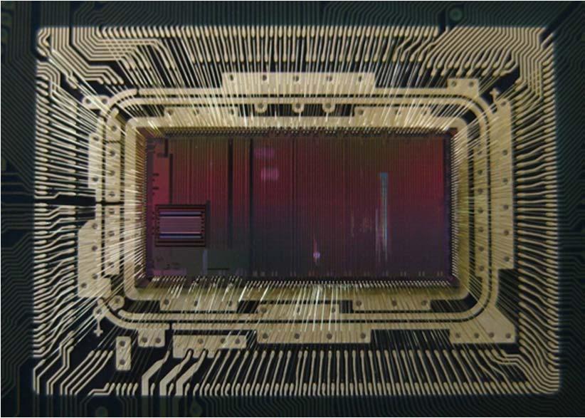
23 Proposed Weight Controlled Capacitor Array Sub-ADC controls the capacitor weight. Load capacitance is reduced from 36C u to 16C u (3bit). 1a V oa 2a 1a V xa 2a 16C u 16C u 1b V ob 2b 1b V xb 2b Total:16Cu 23
24 Weight Controlled Capacitor Array Offset voltage can be cancelled in interpolation phase V x m m n G a V V G V V in ra n m n b in rb V V oa ob V ' V ' oa ob G G a b G G a b V V in in V V V V ra rb off_a off_b V V off_a off_b G a, G b : Gain of A 1a and A 1b V oa, V ob : Output voltage V off_a, V off_b : Offset voltage V ra, V rb : Reference voltage m, n : Capacitor weight 24
25 Interpolated Output V oa V xa 1bit redundancy V x V xa V xb V oa V ob V xb CMP2 V ob 1 37 mc nc mc nc V oa V ob V in V xa 25
26 Sub-ADC Structure Gate-width-weighted interpolation comparators with capacitive offset calibration is used. Offset voltage < 2 mv () 1a CLK DD OUTP W a W b W a W b OUTN V INPa V INPb V INNa V INNb 1b 2nd 1 st stage Sense 2 nd stage Latch [1] V. Giannini, ISSCC 2008 [5] Y. Asada, A-SSCC
27 Requirements for An Amplifier Absolute Gain error No error Offset voltage DNL error Offset voltage < 1LSB Offset voltage can be negrected by output offset cancel technique. Gain mismatch DNL error Linearity DNL and INL error 27
28 Amplifier : Schematic 1st stage amplifier require good linearity =>CMOS input with source degenerations Gain mismatch < 2.1%(3) 28
29 Amplifiers : Simulation results V out a 1 V in a 3 V 3 in 1st stage a 3 /a 1 < 1.3 2nd stage a 3 /a 1 <
30 Gain matching requirement Gain mismatch of 1st stage amplifiers < 2.1%(3s) ENOB [bit] G-G G+G G/G (%) 30
31 Linearity Requirement ENOB [bit] st stage a 3 /a 1 < 1.3, 2nd stage a 3 /a 1 < in a3/a1 V out a 1 V in a 3 V 31

32 Chip photo 90 nm 10M1P CMOS technology Chip area of 0.46mm m Timing generator & Clock lines 415 m 5 th Logic 4 th stage 3 rd stage 2 nd stage 1 st stage 32
33 DNL, INL This periodical error is due to bad layout, not essential issue. DNL [LSB] INL [LSB] OUTPUT CODE OUTPUT CODE DNL +0.9/-0.6 INL +1.4/
34 Sampling Frequency vs. SNDR Input Frequency = 1 MHz 34
35 Input Frequency vs. SNDR Sampling Frequency = 320 MS/s 35
36 Performance summary This Work [2] [6] [7] Resolution (bit) F sample (MS/s) V DD (V) Power (mw) ENOB peak (bit) FoM Fs / FoM ERBW (pj/c.-s) 0.35 / /0.44 Technology (nm) Active Area (mm 2 ) Amplifier type Open Closed Closed Closed Linearity Compensation No Yes No Yes [2] A. Verma and B. Razavi, IEEE J. Solid-State Circuits, vol. 44, Nov., [6] S. Lee, Y. Jeon, K. Kim, J. Kwon, J. Kim, J. Moon, and W. Lee, ISSCC, [7] H. Chen, W. Shen, W. Cheng, and H. Chen, A-SSCC,
37 Conclusions An interpolated pipelined ADC using open-loop amplifier has been proposed. Interpolation architecture G/G < 5% for 10bit Using simple open-loop amplifiers enables high speed operation No need of a linearity compensation Weight Controlled Capacitor Array Load capacitance is reduced from 36C u to 16C u Offset voltage of the amplifier can be cancelled 10bit, 320MS/s, 40 mw ADC has been realized 37
38 Future Prospect Issue: Need twice larger circuits Same capacitance as for the conventional pipeline ADC can be used by modifying circuits. Area and power can be reduced, since lower bandwidth is acceptable. Still need the pipelined ADC? SAR ADC: lowest FoM, but low f s and low resolution. SAR-Pipeline: higher resolution, but lower f s due to multi step conversions. Interleaving: effective for low resolution ADC, but need totally large capacitance.
A 0.55 V 7-bit 160 MS/s Interpolated Pipeline ADC Using Dynamic Amplifiers
 A 0.55 V 7-bit 160 MS/s Interpolated Pipeline ADC Using Dynamic Amplifiers James Lin, Daehwa Paik, Seungjong Lee, Masaya Miyahara, and Akira Matsuzawa Tokyo Institute of Technology, Japan Matsuzawa & Okada
A 12-bit Interpolated Pipeline ADC using Body Voltage Controlled Amplifier
 A 12-bit Interpolated Pipeline ADC using Body Voltage Controlled Amplifier Hyunui Lee, Masaya Miyahara, and Akira Matsuzawa Tokyo Institute of Technology, Japan Outline Background Body voltage controlled
A 6-bit Subranging ADC using Single CDAC Interpolation
 A 6-bit Subranging ADC using Single CDAC Interpolation Hyunui Lee, Masaya Miyahara, and Akira Matsuzawa Tokyo Institute of Technology, Japan Outline Background Interpolation techniques 6-bit, 500 MS/s
A Low-Noise Self-Calibrating Dynamic Comparator for High-Speed ADCs
 1 A Low-Noise Self-Calibrating Dynamic Comparator for High-Speed ADCs Masaya Miyahara, Yusuke Asada, Daehwa Paik and Akira Matsuzawa Tokyo Institute of Technology, Japan Outline 2 Motivation The Calibration
A Low-Offset Latched Comparator Using Zero-Static Power Dynamic Offset Cancellation Technique
 1 A Low-Offset Latched Comparator Using Zero-Static Power Dynamic Offset Cancellation Technique Masaya Miyahara and Akira Matsuzawa Tokyo Institute of Technology, Japan 2 Outline Motivation Design Concept
A 35 fj 10b 160 MS/s Pipelined- SAR ADC with Decoupled Flip- Around MDAC and Self- Embedded Offset Cancellation
 Y. Zu, C.- H. Chan, S.- W. Sin, S.- P. U, R.P. Martins, F. Maloberti: "A 35 fj 10b 160 MS/s Pipelined-SAR ADC with Decoupled Flip-Around MDAC and Self- Embedded Offset Cancellation"; IEEE Asian Solid-
Scalable and Synthesizable. Analog IPs
 Scalable and Synthesizable Analog IPs Akira Matsuzawa Tokyo Institute of Technology Background and Motivation 1 Issues It becomes more difficult to obtain good analog IPs Insufficient design resources
RMO1C-1. Indoor and Outdoor Millimeter Wave Systems and RF/BB SoCs
 RMO1C-1 1 Indoor and Outdoor Millimeter Wave Systems and RF/BB SoCs Akira Matsuzawa and Kenich Okada Tokyo Institute of Technology O-Okayama, Meguro-ku, Tokyo 152-8552, Japan Matsuzawa & Okada Lab. Outline
Asynchronous SAR ADC: Past, Present and Beyond. Mike Shuo-Wei Chen University of Southern California MWSCAS 2014
 Asynchronous SAR ADC: Past, Present and Beyond Mike Shuo-Wei Chen University of Southern California MWSCAS 2014 1 Roles of ADCs Responsibility of ADC is increasing more BW, more dynamic range Potentially
A 9.35-ENOB, 14.8 fj/conv.-step Fully- Passive Noise-Shaping SAR ADC
 A 9.35-ENOB, 14.8 fj/conv.-step Fully- Passive Noise-Shaping SAR ADC Zhijie Chen, Masaya Miyahara, Akira Matsuzawa Tokyo Institute of Technology Symposia on VLSI Technology and Circuits Outline Background
A 15.5 db, Wide Signal Swing, Dynamic Amplifier Using a Common- Mode Voltage Detection Technique
 A 15.5 db, Wide Signal Swing, Dynamic Amplifier Using a Common- Mode Voltage Detection Technique James Lin, Masaya Miyahara and Akira Matsuzawa Tokyo Institute of Technology, Japan Matsuzawa & Okada Laḃ
DESIGN AND PERFORMANCE VERIFICATION OF CURRENT CONVEYOR BASED PIPELINE A/D CONVERTER USING 180 NM TECHNOLOGY
 DESIGN AND PERFORMANCE VERIFICATION OF CURRENT CONVEYOR BASED PIPELINE A/D CONVERTER USING 180 NM TECHNOLOGY Neha Bakawale Departmentof Electronics & Instrumentation Engineering, Shri G. S. Institute of
1.5 bit-per-stage 8-bit Pipelined CMOS A/D Converter for Neuromophic Vision Processor
 1.5 bit-per-stage 8-bit Pipelined CMOS A/D Converter for Neuromophic Vision Processor Yilei Li, Li Du 09212020027@fudan.edu.cn Abstract- Neuromorphic vision processor is an electronic implementation of
A 130mW 100MS/s Pipelined ADC with 69dB SNDR Enabled by Digital Harmonic Distortion Correction. Andrea Panigada, Ian Galton
 A 130mW 100MS/s Pipelined ADC with 69dB SNDR Enabled by Digital Harmonic Distortion Correction Andrea Panigada, Ian Galton University of California at San Diego, La Jolla, CA INTEGRATED SIGNAL PROCESSING
EE247 Lecture 23. Advanced calibration techniques. Compensating inter-stage amplifier non-linearity Calibration via parallel & slow ADC
 EE247 Lecture 23 Pipelined ADCs Combining the bits Stage implementation Circuits Noise budgeting Advanced calibration techniques Compensating inter-stage amplifier non-linearity Calibration via parallel
RECENTLY, low-voltage and low-power circuit design
 IEEE TRANSACTIONS ON CIRCUITS AND SYSTEMS II: EXPRESS BRIEFS, VOL. 55, NO. 4, APRIL 2008 319 A Programmable 0.8-V 10-bit 60-MS/s 19.2-mW 0.13-m CMOS ADC Operating Down to 0.5 V Hee-Cheol Choi, Young-Ju
A stability-improved single-opamp third-order ΣΔ modulator by using a fully-passive noise-shaping SAR ADC and passive adder
 A stability-improved single-opamp third-order ΣΔ modulator by using a fully-passive noise-shaping SAR ADC and passive adder Zhijie Chen, Masaya Miyahara, and Akira Matsuzawa Tokyo Institute of Technology,
A 42 fj 8-bit 1.0-GS/s folding and interpolating ADC with 1 GHz signal bandwidth
 LETTER IEICE Electronics Express, Vol.11, No.2, 1 9 A 42 fj 8-bit 1.0-GS/s folding and interpolating ADC with 1 GHz signal bandwidth Mingshuo Wang a), Fan Ye, Wei Li, and Junyan Ren b) State Key Laboratory
Technology Trend of Ultra-High Data Rate Wireless CMOS Transceivers
 2017.07.03 Technology Trend of Ultra-High Data Rate Wireless CMOS Transceivers Akira Matsuzawa and Kenichi Okada Tokyo Institute of Technology Contents 1 Demand for high speed data transfer Developed high
High Data Rate 60 GHz CMOS Transceiver Design
 High Data Rate 6 GHz CMOS Transceiver Design Akira Matsuzawa Department of Physical Electronics Graduate School of Science and Electronics Tokyo Institute of Technology, O-okayama, Meguro-ku, Tokyo, 152-8552,
A Rail-to-Rail Input 12b 2 MS/s 0.18 µm CMOS Cyclic ADC for Touch Screen Applications
 160 HEE-CHEOL CHOI et al : A RAIL-TO-RAIL INPUT 12B 2 MS/S 0.18 µm CMOS CYCLIC ADC FOR TOUCH SCREEN APPLICATIONS A Rail-to-Rail Input 12b 2 MS/s 0.18 µm CMOS Cyclic ADC for Touch Screen Applications Hee-Cheol
A 80Ms/sec 10bit PIPELINED ADC Using 1.5Bit Stages And Built-in Digital Error Correction Logic
 A 80Ms/sec 10bit PIPELINED ADC Using 1.5Bit Stages And Built-in Digital Error Correction Logic Abstract P.Prasad Rao 1 and Prof.K.Lal Kishore 2, 1 Research Scholar, JNTU-Hyderabad prasadrao_hod@yahoo.co.in
A 0.7 V-to-1.0 V 10.1 dbm-to-13.2 dbm 60-GHz Power Amplifier Using Digitally- Assisted LDO Considering HCI Issues
 A 0.7 V-to-1.0 V 10.1 dbm-to-13.2 dbm 60-GHz Power Amplifier Using Digitally- Assisted LDO Considering HCI Issues Rui Wu, Yuuki Tsukui, Ryo Minami, Kenichi Okada, and Akira Matsuzawa Tokyo Institute of
Low-Power Pipelined ADC Design for Wireless LANs
 Low-Power Pipelined ADC Design for Wireless LANs J. Arias, D. Bisbal, J. San Pablo, L. Quintanilla, L. Enriquez, J. Vicente, J. Barbolla Dept. de Electricidad y Electrónica, E.T.S.I. de Telecomunicación,
2008 IEEE ASIA PACIFIC CONFERENCE ON CIRCUITS AND SYSTEMS
 2008 IEEE ASIA PACIFIC CONFERENCE ON CIRCUITS AND SYSTEMS November 30 - December 3, 2008 Venetian Macao Resort-Hotel Macao, China IEEE Catalog Number: CFP08APC-USB ISBN: 978-1-4244-2342-2 Library of Congress:
A 10-Bit 500-MS/s 55-mW CMOS ADC Ashutosh Verma, Member, IEEE, and Behzad Razavi, Fellow, IEEE
 IEEE JOURNAL OF SOLID-STATE CIRCUITS, VOL. 44, NO. 11, NOVEMBER 2009 3039 A 10-Bit 500-MS/s 55-mW CMOS ADC Ashutosh Verma, Member, IEEE, and Behzad Razavi, Fellow, IEEE Abstract A pipelined ADC incorporates
ISSCC 2003 / SESSION 20 / WIRELESS LOCAL AREA NETWORKING / PAPER 20.5
 ISSCC 2003 / SESSION 20 / WIRELESS LOCAL AREA NETWORKING / PAPER 20.5 20.5 A 2.4GHz CMOS Transceiver and Baseband Processor Chipset for 802.11b Wireless LAN Application George Chien, Weishi Feng, Yungping
A Two- Bit- per- Cycle Successive- Approximation ADC with Background Offset Calibration
 M. Casubolo, M. Grassi, A. Lombardi, F. Maloberti, P. Malcovati: "A Two-Bit-per- Cycle Successive-Approximation ADC with Background Calibration"; 15th IEEE Int. Conf. on Electronics, Circuits and Systems,
Index terms: Analog to Digital conversion, capacitor sharing, high speed OPAMP-sharing pipelined analog to digital convertor, Low power.
 Pipeline ADC using Switched Capacitor Sharing Technique with 2.5 V, 10-bit Ankit Jain Dept. of Electronics and Communication, Indore Institute of Science & Technology, Indore, India Abstract: This paper
Design of Pipeline Analog to Digital Converter
 Design of Pipeline Analog to Digital Converter Vivek Tripathi, Chandrajit Debnath, Rakesh Malik STMicroelectronics The pipeline analog-to-digital converter (ADC) architecture is the most popular topology
Design Challenges of Analog-to-Digital Converters in Nanoscale CMOS
 IEICE TRANS. ELECTRON., VOL.E90 C, NO.4 APRIL 2007 779 INVITED PAPER Special Section on Low-Power, High-Speed LSIs and Related Technologies Design Challenges of Analog-to-Digital Converters in Nanoscale
A Digitally-Calibrated 20-Gb/s 60-GHz Direct-Conversion Transceiver in 65-nm CMOS
 A Digitally-Calibrated 20-Gb/s 60-GHz Direct-Conversion Transceiver in 65-nm CMOS Seitaro Kawai, Ryo Minami, Yuki Tsukui, Yasuaki Takeuchi, Hiroki Asada, Ahmed Musa, Rui Murakami, Takahiro Sato, Qinghong
Architectures and circuits for timeinterleaved. Sandeep Gupta Teranetics, Santa Clara, CA
 Architectures and circuits for timeinterleaved ADC s Sandeep Gupta Teranetics, Santa Clara, CA Outline Introduction to time-interleaved architectures. Conventional Sampling architectures and their application
A 2-bit/step SAR ADC structure with one radix-4 DAC
 A 2-bit/step SAR ADC structure with one radix-4 DAC M. H. M. Larijani and M. B. Ghaznavi-Ghoushchi a) School of Engineering, Shahed University, Tehran, Iran a) ghaznavi@shahed.ac.ir Abstract: In this letter,
STATE-OF-THE-ART read channels in high-performance
 258 IEEE JOURNAL OF SOLID-STATE CIRCUITS, VOL. 42, NO. 2, FEBRUARY 2007 A 6-bit 800-MS/s Pipelined A/D Converter With Open-Loop Amplifiers Ding-Lan Shen, Student Member, IEEE, and Tai-Cheng Lee, Member,
/$ IEEE
 894 IEEE TRANSACTIONS ON CIRCUITS AND SYSTEMS I: REGULAR PAPERS, VOL. 56, NO. 5, MAY 2009 A 1.2-V 12-b 120-MS/s SHA-Free Dual-Channel Nyquist ADC Based on Midcode Calibration Hee-Cheol Choi, Young-Ju Kim,
CHAPTER 3 DESIGN OF PIPELINED ADC USING SCS-CDS AND OP-AMP SHARING TECHNIQUE
 CHAPTER 3 DESIGN OF PIPELINED ADC USING SCS-CDS AND OP-AMP SHARING TECHNIQUE 3.1 INTRODUCTION An ADC is a device which converts a continuous quantity into discrete digital signal. Among its types, pipelined
12-bit 50/100/125 MSPS 1-channel ADC
 SPECIFICATION 1 FEATURES TSMC CMOS 65 nm High speed pipelined ADC Resolution 12 bit Conversion rate 50/100/125 MHz Different power supplies for digital (1.2 V) and analog (1.2 V) parts Low standby current
EE247 Lecture 22. Figures of merit (FOM) and trends for ADCs How to use/not use FOM. EECS 247 Lecture 22: Data Converters 2004 H. K.
 and trends for ADCs How to use/not use FOM. EECS 247 Lecture 22: Data Converters 2004 H. K.") EE247 Lecture 22 Pipelined ADCs Combining the bits Stage implementation Circuits Noise budgeting Figures of merit (FOM) and trends for ADCs How to use/not use FOM Oversampled ADCs EECS 247 Lecture 22:
EE247 Lecture 22 Pipelined ADCs Combining the bits Stage implementation Circuits Noise budgeting Figures of merit (FOM) and trends for ADCs How to use/not use FOM Oversampled ADCs EECS 247 Lecture 22:
A SAR-Assisted Two-Stage Pipeline ADC Chun C. Lee, Member, IEEE, and Michael P. Flynn, Senior Member, IEEE
 IEEE JOURNAL OF SOLID-STATE CIRCUITS, VOL. 46, NO. 4, APRIL 2011 859 A SAR-Assisted Two-Stage Pipeline ADC Chun C. Lee, Member, IEEE, and Michael P. Flynn, Senior Member, IEEE Abstract Successive approximation
Design of an Assembly Line Structure ADC
 Design of an Assembly Line Structure ADC Chen Hu 1, Feng Xie 1,Ming Yin 1 1 Department of Electronic Engineering, Naval University of Engineering, Wuhan, China Abstract This paper presents a circuit design
Another way to implement a folding ADC
 Another way to implement a folding ADC J. Van Valburg and R. van de Plassche, An 8-b 650 MHz Folding ADC, IEEE JSSC, vol 27, #12, pp. 1662-6, Dec 1992 Coupled Differential Pair J. Van Valburg and R. van
Summary Last Lecture
 EE247 Lecture 23 Converters Techniques to reduce flash complexity Interpolating (continued) Folding Multi-Step s Two-Step flash Pipelined s EECS 247 Lecture 23: Data Converters 26 H.K. Page Summary Last
ISSCC 2004 / SESSION 25 / HIGH-RESOLUTION NYQUIST ADCs / 25.4
 ISSCC 2004 / SESSION 25 / HIGH-RESOLUTION NYQUIST ADCs / 25.4 25.4 A 1.8V 14b 10MS/s Pipelined ADC in 0.18µm CMOS with 99dB SFDR Yun Chiu, Paul R. Gray, Borivoje Nikolic University of California, Berkeley,
IMPLEMENTING THE 10-BIT, 50MS/SEC PIPELINED ADC
 98 CHAPTER 5 IMPLEMENTING THE 0-BIT, 50MS/SEC PIPELINED ADC 99 5.0 INTRODUCTION This chapter is devoted to describe the implementation of a 0-bit, 50MS/sec pipelined ADC with different stage resolutions
Design of Analog Integrated Systems (ECE 615) Outline
 Outline") Design of Analog Integrated Systems (ECE 615) Lecture 9 SAR and Cyclic (Algorithmic) Analog-to-Digital Converters Ayman H. Ismail Integrated Circuits Laboratory Ain Shams University Cairo, Egypt ayman.hassan@eng.asu.edu.eg
Design of Analog Integrated Systems (ECE 615) Lecture 9 SAR and Cyclic (Algorithmic) Analog-to-Digital Converters Ayman H. Ismail Integrated Circuits Laboratory Ain Shams University Cairo, Egypt ayman.hassan@eng.asu.edu.eg
SUCCESSIVE approximation register (SAR) analog-todigital
 analog-todigital") IEEE JOURNAL OF SOLID-STATE CIRCUITS, VOL. 45, NO. 4, APRIL 2010 731 A 10-bit 50-MS/s SAR ADC With a Monotonic Capacitor Switching Procedure Chun-Cheng Liu, Student Member, IEEE, Soon-Jyh Chang, Member,
IEEE JOURNAL OF SOLID-STATE CIRCUITS, VOL. 45, NO. 4, APRIL 2010 731 A 10-bit 50-MS/s SAR ADC With a Monotonic Capacitor Switching Procedure Chun-Cheng Liu, Student Member, IEEE, Soon-Jyh Chang, Member,
Digital Calibration for Current-Steering DAC Linearity Enhancement
 Digital Calibration for Current-Steering DAC Linearity Enhancement Faculty of Science and Technology, Division of Electronics & Informatics Gunma University Shaiful Nizam Mohyar, Haruo Kobayashi Gunma
Acronyms. ADC analog-to-digital converter. BEOL back-end-of-line
 Acronyms ADC analog-to-digital converter BEOL back-end-of-line CDF cumulative distribution function CMOS complementary metal-oxide-semiconductor CPU central processing unit CR charge-redistribution CS
Pipelined Analog-to-Digital converter (ADC)
") Analog Integr Circ Sig Process (2012) 63:495 501 DOI 10.1007/s10470-010-9453-0 MIXED SIGNAL LETTER Pipelined Analog-to-Digital converter (ADC) Mingjun Fan Junyan Ren Ning Li Fan Ye Jun Xu Abstract A set
Analog Integr Circ Sig Process (2012) 63:495 501 DOI 10.1007/s10470-010-9453-0 MIXED SIGNAL LETTER Pipelined Analog-to-Digital converter (ADC) Mingjun Fan Junyan Ren Ning Li Fan Ye Jun Xu Abstract A set
A VCO-Based ADC Employing a Multi- Phase Noise-Shaping Beat Frequency Quantizer for Direct Sampling of Sub-1mV Input Signals
 A VCO-Based ADC Employing a Multi- Phase Noise-Shaping Beat Frequency Quantizer for Direct Sampling of Sub-1mV Input Signals Bongjin Kim, Somnath Kundu, Seokkyun Ko and Chris H. Kim University of Minnesota,
Summary Last Lecture
 EE247 Lecture 23 Converters Techniques to reduce flash complexity Interpolating (continued) Folding Multi-Step s Two-Step flash Pipelined s EECS 247 Lecture 23: Data Converters 26 H.K. Page 1 Summary Last
A Two-channel 10b 160 MS/s 28 nm CMOS Asynchronous Pipelined-SAR ADC with Low Channel Mismatch
 JOURNAL OF SEMICONDUCTOR TECHNOLOGY AND SCIENCE, VOL.17, NO.5, OCTOBER, 2017 ISSN(Print) 1598-1657 https://doi.org/10.5573/jsts.2017.17.5.636 ISSN(Online) 2233-4866 A Two-channel 10b 160 MS/s 28 nm CMOS
Design of Low-Offset Voltage Dynamic Latched Comparator
 Apr. 212, Vol. 2(4) pp: 585-59 Design of Low-Offset Voltage Dynamic Latched Comparator Mayank Nema, Rachna Thakur Assistant Professor, Department of ECE Sagar Institute of Science, Technology & Research,
A 4 GSample/s 8-bit ADC in. Ken Poulton, Robert Neff, Art Muto, Wei Liu, Andrew Burstein*, Mehrdad Heshami* Agilent Laboratories Palo Alto, California
 A 4 GSample/s 8-bit ADC in 0.35 µm CMOS Ken Poulton, Robert Neff, Art Muto, Wei Liu, Andrew Burstein*, Mehrdad Heshami* Agilent Laboratories Palo Alto, California 1 Outline Background Chip Architecture
A Successive Approximation ADC based on a new Segmented DAC
 A Successive Approximation ADC based on a new Segmented DAC segmented current-mode DAC successive approximation ADC bi-direction segmented current-mode DAC DAC INL 0.47 LSB DNL 0.154 LSB DAC 3V 8 2MS/s
EE247 Lecture 23. EECS 247 Lecture 23 Pipelined ADCs 2008 H.K. Page 1. Pipeline ADC Block Diagram DAC ADC. V res2. Stage 2 B 2.
 EE247 Lecture 23 Pipelined ADCs (continued) Effect gain stage, sub-dac non-idealities on overall ADC performance Digital calibration (continued) Correction for inter-stage gain nonlinearity Implementation
A 1MHz-64MHz Active RC TI-LPF with Variable Gain for SDR Receiver in 65-nm CMOS
 2017 5th International Conference on Computer, Automation and Power Electronics (CAPE 2017) A 1MHz-64MHz Active RC TI-LPF with Variable Gain for SDR Receiver in 65-nm CMOS Chaoxuan Zhang1, a, *, Xunping
CMOS ADC & DAC Principles
 CMOS ADC & DAC Principles Willy Sansen KULeuven, ESAT-MICAS Leuven, Belgium willy.sansen@esat.kuleuven.be Willy Sansen 10-05 201 Table of contents Definitions Digital-to-analog converters Resistive Capacitive
620 IEEE JOURNAL OF SOLID-STATE CIRCUITS, VOL. 45, NO. 3, MARCH /$ IEEE
 620 IEEE JOURNAL OF SOLID-STATE CIRCUITS, VOL. 45, NO. 3, MARCH 2010 A 12 bit 50 MS/s CMOS Nyquist A/D Converter With a Fully Differential Class-AB Switched Op-Amp Young-Ju Kim, Hee-Cheol Choi, Gil-Cho
WITH the recent development of communication systems
 IEEE TRANSACTIONS ON CIRCUITS AND SYSTEMS I: REGULAR PAPERS, VOL. 58, NO. 9, SEPTEMBER 2011 2127 A 12b 50 MS/s 21.6 mw 0.18 m CMOS ADC Maximally Sharing Capacitors and Op-Amps Kyung-Hoon Lee, Student Member,
Integrated Microsystems Laboratory. Franco Maloberti
 University of Pavia Integrated Microsystems Laboratory Power Efficient Data Convertes Franco Maloberti franco.maloberti@unipv.it OUTLINE Introduction Managing the noise power budget Challenges of State-of-the-art
PAPER A Single Amplifier-Based 12-bit 100 MS/s 1V19mW0.13µm CMOS ADC with Various Power and Area Minimized Circuit Techniques
 1282 PAPER A Single Amplifier-Based 12-bit 100 MS/s 1V19mW0.13µm CMOS ADC with Various Power and Area Minimized Circuit Techniques Byeong-Woo KOO, Member, Seung-Jae PARK, Gil-Cho AHN, and Seung-Hoon LEE
Fundamentals of Data Conversion: Part I.1
 Fundamentals of Data Conversion: Part I.1 Sebastian Hoyos http://ece.tamu.edu/~hoyos/ Several of these slides were provided by Dr. Jose Silva-Martinez and Dr. Jun Zhou Outline Fundamentals of Analog-to-Digital
CMOS Analog to Digital Converters : State-of-the-Art and Perspectives in Digital Communications ADC
 CMOS Analog to Digital Converters : State-of-the-Art and Perspectives in Digital Communications ADC Hussein Fakhoury and Hervé Petit C²S Research Group Presentation Outline Introduction Basic concepts
A SWITCHED-CAPACITOR POWER AMPLIFIER FOR EER/POLAR TRANSMITTERS
 A SWITCHED-CAPACITOR POWER AMPLIFIER FOR EER/POLAR TRANSMITTERS Sang-Min Yoo, Jeffrey Walling, Eum Chan Woo, David Allstot University of Washington, Seattle, WA Submission Highlight A fully-integrated
Pipelined Analog-to-Digital Converters
 Department of Electrical and Computer Engineering Pipelined Analog-to-Digital Converters Vishal Saxena Vishal Saxena -1- Multi-Step A/D Conversion Basics Vishal Saxena -2-2 Motivation for Multi-Step Converters
High-Speed Analog to Digital Converters. ELCT 1003:High Speed ADCs
 High-Speed Analog to Digital Converters Ann Kotkat Barbara Georgy Mahmoud Tantawi Ayman Sakr Heidi El-Feky Nourane Gamal 1 Outline Introduction. Process of ADC. ADC Specifications. Flash ADC. Pipelined
A 12b 50MS/s 2.1mW SAR ADC with redundancy and digital background calibration
 A b 5MS/s.mW SAR ADC with redundancy and digital background calibration The MIT Faculty has made this article openly available. Please share how this access benefits you. Your story matters. Citation As
HIGH-SPEED low-resolution analog-to-digital converters
 244 IEEE TRANSACTIONS ON CIRCUITS AND SYSTEMS II: EXPRESS BRIEFS, VOL. 64, NO. 3, MARCH 2017 A 0.95-mW 6-b 700-MS/s Single-Channel Loop-Unrolled SAR ADC in 40-nm CMOS Long Chen, Student Member, IEEE, Kareem
Wideband Sampling by Decimation in Frequency
 Wideband Sampling by Decimation in Frequency Martin Snelgrove http://www.kapik.com 192 Spadina Ave. Suite 218 Toronto, Ontario, M5T2C2 Canada Copyright Kapik Integration 2011 WSG: New Architectures for
ISSN:
 1391 DESIGN OF 9 BIT SAR ADC USING HIGH SPEED AND HIGH RESOLUTION OPEN LOOP CMOS COMPARATOR IN 180NM TECHNOLOGY WITH R-2R DAC TOPOLOGY AKHIL A 1, SUNIL JACOB 2 1 M.Tech Student, 2 Associate Professor,
Figure 1 Typical block diagram of a high speed voltage comparator.
 IOSR Journal of VLSI and Signal Processing (IOSR-JVSP) Volume 6, Issue 6, Ver. I (Nov. - Dec. 2016), PP 58-63 e-issn: 2319 4200, p-issn No. : 2319 4197 www.iosrjournals.org Design of Low Power Efficient
SUCCESSIVE approximation register (SAR) analog-todigital
 analog-todigital") 426 IEEE TRANSACTIONS ON CIRCUITS AND SYSTEMS II: EXPRESS BRIEFS, VOL. 62, NO. 5, MAY 2015 A Novel Hybrid Radix-/Radix-2 SAR ADC With Fast Convergence and Low Hardware Complexity Manzur Rahman, Arindam
426 IEEE TRANSACTIONS ON CIRCUITS AND SYSTEMS II: EXPRESS BRIEFS, VOL. 62, NO. 5, MAY 2015 A Novel Hybrid Radix-/Radix-2 SAR ADC With Fast Convergence and Low Hardware Complexity Manzur Rahman, Arindam
A 12b 100 MS/s Three-Step Hybrid Pipeline ADC Based on Time-Interleaved SAR ADCs
 JOURNAL OF SEMICONDUCTOR TECHNOLOGY AND SCIENCE, VOL.14, NO.2, APRIL, 2014 http://dx.doi.org/10.5573/jsts.2014.14.2.189 A 12b 100 MS/s Three-Step Hybrid ADC Based on Time-Interleaved SAR ADCs Jun-Sang
10.1: A 4 GSample/s 8b ADC in 0.35-um CMOS
 10.1: A 4 GSample/s 8b ADC in 0.35-um CMOS Ken Poulton, Robert Neff, Art Muto, Wei Liu*, Andy Burstein**, Mehrdad Heshami*** Agilent Technologies, Palo Alto, CA *Agilent Technologies, Colorado Springs,
BER-optimal ADC for Serial Links
 BER-optimal ADC for Serial Links Speaker Name: Yingyan Lin Co-authors: Min-Sun Keel, Adam Faust, Aolin Xu, Naresh R. Shanbhag, Elyse Rosenbaum, and Andrew Singer Advisor s name: Naresh R. Shanbhag Affiliation:
A 1.7-to-2.2GHz Full-Duplex Transceiver System with >50dB Self-Interference Cancellation over 42MHz Bandwidth
 A 1.7-to-2.2GHz Full-Duplex Transceiver System with >50dB Self-Interference Cancellation Tong Zhang, Ali Najafi, Chenxin Su, Jacques C. Rudell University of Washington, Seattle Feb. 8, 2017 International
FUNDAMENTALS OF ANALOG TO DIGITAL CONVERTERS: PART I.1
 FUNDAMENTALS OF ANALOG TO DIGITAL CONVERTERS: PART I.1 Many of these slides were provided by Dr. Sebastian Hoyos January 2019 Texas A&M University 1 Spring, 2019 Outline Fundamentals of Analog-to-Digital
EFFICIENT LOW POWER DYNAMIC COMPARATOR FOR HIGH SPEED ADC s
 EFFICIENT LOW POWER DYNAMIC COMPARATOR FOR HIGH SPEED ADC s B.Padmavathi, ME (VLSI Design), Anand Institute of Higher Technology, Chennai, India krishypadma@gmail.com Abstract In electronics, a comparator
THE pipelined ADC architecture has been adopted into
 1468 IEEE JOURNAL OF SOLID-STATE CIRCUITS, VOL. 39, NO. 9, SEPTEMBER 2004 A 1.8-V 67-mW 10-bit 100-MS/s Pipelined ADC Using Time-Shifted CDS Technique Jipeng Li, Member, IEEE, and Un-Ku Moon, Senior Member,
A 10 bit, 1.8 GS/s Time Interleaved Pipeline ADC
 A 10 bit, 1.8 GS/s Time Interleaved Pipeline ADC M. Åberg 2, A. Rantala 2, V. Hakkarainen 1, M. Aho 1, J. Riikonen 1, D. Gomes Martin 2, K. Halonen 1 1 Electronic Circuit Design Laboratory Helsinki University
Design of Low Power High Speed Fully Dynamic CMOS Latched Comparator
 International Journal of Engineering Research and Development e-issn: 2278-067X, p-issn: 2278-800X, www.ijerd.com Volume 10, Issue 4 (April 2014), PP.01-06 Design of Low Power High Speed Fully Dynamic
Tuesday, March 1st, 9:15 11:00. Snorre Aunet Nanoelectronics group Department of Informatics University of Oslo.
 Nyquist Analog to Digital it Converters Tuesday, March 1st, 9:15 11:00 Snorre Aunet (sa@ifi.uio.no) Nanoelectronics group Department of Informatics University of Oslo 3.1 Introduction 3.1.1 DAC applications
DESIGN AND IMPLEMENTATION OF A LOW VOLTAGE LOW POWER DOUBLE TAIL COMPARATOR
 DESIGN AND IMPLEMENTATION OF A LOW VOLTAGE LOW POWER DOUBLE TAIL COMPARATOR 1 C.Hamsaveni, 2 R.Ramya 1,2 PG Scholar, Department of ECE, Hindusthan Institute of Technology, Coimbatore(India) ABSTRACT Comparators
Modeling and Implementation of A 6-Bit, 50MHz Pipelined ADC in CMOS
 Master s Thesis Modeling and Implementation of A 6-Bit, 50MHz Pipelined ADC in CMOS Qazi Omar Farooq Department of Electrical and Information Technology, Faculty of Engineering, LTH, Lund University, 2016.
DESIGN OF A 500MHZ, 4-BIT LOW POWER ADC FOR UWB APPLICATION
 DESIGN OF A 500MHZ, 4-BIT LOW POWER ADC FOR UWB APPLICATION SANTOSH KUMAR PATNAIK 1, DR. SWAPNA BANERJEE 2 1,2 E & ECE Department, Indian Institute of Technology, Kharagpur, Kharagpur, India Abstract-This
A 1.2V 8 BIT SAR ANALOG TO DIGITAL CONVERTER IN 90NM CMOS
 A 1.2V 8 BIT SAR ANALOG TO DIGITAL CONVERTER IN 90NM CMOS Shruti Gatade 1, M. Nagabhushan 2, Manjunath.R 3 1,3 Student, Department of ECE, M S Ramaiah Institute of Technology, Bangalore (India) 2 Assistant
A Low-Power 6-b Integrating-Pipeline Hybrid Analog-to-Digital Converter
 A Low-Power 6-b Integrating-Pipeline Hybrid Analog-to-Digital Converter Quentin Diduck, Martin Margala * Electrical and Computer Engineering Department 526 Computer Studies Bldg., PO Box 270231 University
Design of low-loss 60 GHz integrated antenna switch in 65 nm CMOS
 LETTER IEICE Electronics Express, Vol.15, No.7, 1 10 Design of low-loss 60 GHz integrated antenna switch in 65 nm CMOS Korkut Kaan Tokgoz a), Seitaro Kawai, Kenichi Okada, and Akira Matsuzawa Department
A Low Power Analog Front End Capable of Monitoring Knee Movements to Detect Injury
 A Low Power Analog Front End Capable of Monitoring Knee Movements to Detect Injury Garren Boggs, Hua Chen, Sridhar Sivapurapu ECE 6414 Final Presentation Outline Motivation System Overview Analog Front
Circuit Design for a 2.2 GByte/s Memory Interface
 Circuit Design for a 2.2 GByte/s Memory Interface Stefanos Sidiropoulos Work done at Rambus Inc with A. Abhyankar, C. Chen, K. Chang, TJ Chin, N. Hays, J. Kim, Y. Li, G. Tsang, A. Wong, D. Stark Increasing
A Digitally Enhanced 1.8-V 15-b 40- Msample/s CMOS Pipelined ADC
 A Digitally Enhanced.8-V 5-b 4- Msample/s CMOS d ADC Eric Siragusa and Ian Galton University of California San Diego Now with Analog Devices San Diego California Outline Conventional PADC Example Digitally
Design and Implementation of a Low Power Successive Approximation ADC. Xin HUANG, Xiao-ning XIN, Jian REN* and Xin-lei CHEN
 2018 International Conference on Mechanical, Electronic and Information Technology (ICMEIT 2018) ISBN: 978-1-60595-548-3 Design and Implementation of a Low Power Successive Approximation ADC Xin HUANG,
mm-wave Transceiver Challenges for the 5G and 60GHz Standards Prof. Emanuel Cohen Technion
 mm-wave Transceiver Challenges for the 5G and 60GHz Standards Prof. Emanuel Cohen Technion November 11, 11, 2015 2015 1 mm-wave advantage Why is mm-wave interesting now? Available Spectrum 7 GHz of virtually
ISSCC 2004 / SESSION 25 / HIGH-RESOLUTION NYQUIST ADCs / 25.3
 ISSCC 2004 / SESSION 25 / HIGH-RESOLUTION NYQUIST ADCs / 25.3 25.3 A 96dB SFDR 50MS/s Digitally Enhanced CMOS Pipeline A/D Converter K. Nair, R. Harjani University of Minnesota, Minneapolis, MN Analog-to-digital
12-Bit 1-channel 4 MSPS ADC
 SPECIFICATION 1 FEATURES 12-Bit 1-channel 4 MSPS ADC TSMC CMOS 65 nm Resolution 12 bit Single power supplies for digital and analog parts (2.5 V) Sampling rate up to 4 MSPS Standby mode (current consumption
DIGITAL wireless communication applications such as
 IEEE TRANSACTIONS ON CIRCUITS AND SYSTEMS I: REGULAR PAPERS, VOL. 57, NO. 8, AUGUST 2010 1829 An Asynchronous Binary-Search ADC Architecture With a Reduced Comparator Count Ying-Zu Lin, Student Member,
CMOS High Speed A/D Converter Architectures
 CHAPTER 3 CMOS High Speed A/D Converter Architectures 3.1 Introduction In the previous chapter, basic key functions are examined with special emphasis on the power dissipation associated with its implementation.
MOST pipelined analog-to-digital converters (ADCs) employ
 employ") IEEE JOURNAL OF SOLID-STATE CIRCUITS, VOL. 49, NO. 8, AUGUST 2014 1739 A 7.1 mw 1 GS/s ADC With 48 db SNDR at Nyquist Rate Sedigheh Hashemi and Behzad Razavi, Fellow, IEEE Abstract A two-stage pipelined
IEEE JOURNAL OF SOLID-STATE CIRCUITS, VOL. 49, NO. 8, AUGUST 2014 1739 A 7.1 mw 1 GS/s ADC With 48 db SNDR at Nyquist Rate Sedigheh Hashemi and Behzad Razavi, Fellow, IEEE Abstract A two-stage pipelined