Fundamentals of Data Conversion: Part I.1
|
|
|
- Myron Long
- 5 years ago
- Views:
Transcription
1 Fundamentals of Data Conversion: Part I.1 Sebastian Hoyos Several of these slides were provided by Dr. Jose Silva-Martinez and Dr. Jun Zhou
2 Outline Fundamentals of Analog-to-Digital Converters Introduction Sampling and Quantization Quantization noise and distortion INL and DNL Technological related issues Sample and Hold Switching issues S/H Accuracy Active S/H Switch around S/H


3 The Smartphone market Global smartphone market projected to grow Anticipated global unit sales to approach 400 millions in 2013 (market research report from Forward Concepts Co) Projected revenue in 2012: $32.2 billion (source: In-Stat Group)
 nanometric tecnologies FM WiMax & 802.")
4 Multi-standard Wireless Systems Multiple services Reuse circuits as much as possible Power Area Competitiveness GSM WiFi Smaller Cell phone, stronger function, longer battery duration WCDMA Bluetooth Use of digital (analog unfriendly) nanometric tecnologies FM WiMax & GPS

5 Multi-standard Wireless Systems Exponential growth in mobile computing and broadband wireless Major need for high dynamic range, wide-bandwidth, low power ADCs.
6 Bandwidth requirements for higher connectivity Specturm > 45 db DTV IS-95 GSM DECT Bluetooth, b and g UMTS a Frequency (GHz) Higher flexibility on operational frequency and bandwidth, higher blocker rejection, higher dynamic range Receiver Architectures: Super-heterodyne, Low-IF, Direct Conversion, High-IF, Digital Radio
7 What is an Analog-to-Digital Converter (ADC)? Analog Digital Continuous with no apparent discontinuities The way we interpret our surroundings: sound, light, temperature etc ADC Discrete with limited range; based on binary numbers with limited number of bits. The way we mathematically represent and process our world using electronic brain power

8 R. Walden, 1999
9 How does an ADC work? Analog Digital Continuous with no apparent discontinuities x(t) Sampling The way we interpret our surroundings: sound, light, δ(t-nt S ) temperature etc x(nt S ) ADC Quantization x(nt S )+q(nt S ) Discrete with limited range; based Decoding on binary numbers with limited number N bits of bits The 1 way 001 we mathematically represent and process our world using electronic brain power
10 How does an ADC work? Analog x(t) ADC x(n) Digital t nt S x(t) Sampling δ(t-nt S ) x(nt S ) Quantization Quantization noise x(nt S )+q(nt S ) x(n) Decoding N bits δ(n) 2 N Levels separated by 1LSB, 1LSB = V FS* / 2 N nt S nt S * V FS = full scale range, V max -V min
 2009 CCD/ CMOS Image Array AMP")
 CCD/ CMOS Image Array AMP ADC DSP (balance control, black level")
 0.5-0.")
 Some pre-adc analog conditioning ~ 2.")
 12M pixel CCD sensor (high pixel")

11 ADCs: Yesterday vs. Today 2000 Example: Digital photography (8-12b ADCs) 2009 CCD/ CMOS Image Array AMP Balance Control ADC DSP (black level compensation, encoding...etc) CCD/ CMOS Image Array AMP ADC DSP (balance control, black level compensation, image stabilization, exposure levels, noise reduction, lens shading correction, encoding...etc) µm CMOS with 5V supply (moderate gate density and speed in DSPs) 2M pixel CCD sensor (low pixel scanning speed) Some pre-adc analog conditioning ~ 2.5mV / LSB 90nm-180nm CMOS with V supplies (high gate density and speed in DSPs) 12M pixel CCD sensor (high pixel scanning speed) Minimal pre-adc analog conditioning ~ 0.5mV / LSB Faster DSPs capable of performing numerous complex functions are developed thanks to advanced CMOS ADCs are indispensable, but now need to handle smaller signals at higher speeds with similar or higher resolutions. ADCs are becoming the bottleneck for advancement, and new design techniques need to be developed.
 20 18 16 14 12 10 8 6 4 2 Sigma-Delta Pipelined Flash 0.01 0.")

? 4G? HDTV?")
12 ADCs: Tomorrow? ADC IEEE literature survey: Resolution (bits) Sigma-Delta Pipelined Flash Signal Bandwidth (MHz) Pipeline ADC is currently most published architecture Pipeline ADC is breaking the trend set by Sigma- Delta and Flash ADCs Pipeline ADC is breaking the trend set by Sigma- Delta and Flash ADCs, and driven by consumer electronics Pipeline ADC is expected to be a key ADC architecture in future applications Pipeline ADC Applications Today Tomorrow 15M? 20M? From 1080P to 4K (2160P)? 4G? HDTV? The development of new design techniques for high speed, low voltage and low power Pipeline ADCs is crucial to stay on the future applications roadmap


13 Design Challenges of Pipeline ADCs in Advanced CMOS Technologies (Summary) High Speed Low Voltage Low Power Digital Camera Example CCD/ CMOS Image Array AMP ADC DSP (balance control, black level compensation, image stabilization, exposure levels, noise reduction, lens shading correction, encoding...etc) With the added speed of new generations of DSPs, the ADC is becoming the bottleneck for overall system speed in addition to increased speed, the DSP ability to perform more complex tasks will require higher ADC resolutions Reduction of Device size allows for denser integration, but device reliability dictate lower supply voltages Reduced supplies means reduced signal range, which requires a higher ADC accuracy for the same number of bits Many applications are portable and operated from a battery As a potentially power hungry component, the ADC power needs to be reduced to help prolong battery life
14 Super-heterodyne Receiver Antenna RF ( GHz) High IF ( MHz) BPF LNA BPF VGA Baseband (< 20 MHz) LPF Baseband ADC Digital Output LO1 LO2 Invented by Armstrong in 1918 Hardware specific radio architecture Extensive filtering to relax ADC specs Suitable for narrow-band applications
15 Design issues for multi-standard solutions Antenna RF ( GHz) High IF ( MHz) BPF LNA VGA BPF Baseband (< 20 MHz) LPF Baseband ADC Digital Output Limited by flicker noise Not flexible Hardware intensive LO1 LO2 Excessive power at the front-end (Linearity issues) Extensive down conversions: LO and mixers increase both noise and power consumption Extensive filtering: Area, Power and Noise issues Not fully compatible for the Telecoms roadmap
16 Current Multi-standard designs Antenna RF (1-2 GHz) Receiver for standard 1 IF ( MHz) BPF LNA VGA BPF Minimum sharing of blocks Area and power consumption overhead LO1 LO2 Not Flexible at all RF Switch RF (1-2 GHz) Receiver for standard 2 IF ( MHz) BPF LNA VGA BPF Limited number of standards can be accommodated LO1 LO2

17 Introduction to Analog-to-Digital Converters Analog-to-Digital Converters (ADC) are necessary to convert real world signals (which are analog in nature) to their digital equivalents for easy processing. Common applications for ADCs are communication systems, TV receivers, Digital Oscilloscopes, Audio applications.. Analog
18 Efficient radio transceiver: Direct Conversion Antenna Frequency Synthesizer 16-Channel Multiband Digital Receiver RF signal Antenna IF Filter 1 RF Filter 1 LNA & VGA Mixer 80 MHz ADC 1 Optional 4- channel digital receiver 4- channel digital receiver Software Platform DSP RF signal RF Filter 2 LNA & VGA Mixer IF Filter 2 ADC 2 4- channel digital receiver or FPGAs 4- channel digital receiver Direct conversion + broadband ADC (1 receiver per service) Lowpass filter is required (~ mw) bits 80 MHz Lowpass ADC (500 mw from ADI) Bank of receivers, filters and ADCs
19 Recent Approaches to Broadband Receivers Sample rate, downsampling and filtering R. Crochiere and L. Rabiner, Multirate Digital Signal Processing. Englewood Cliffs, NJ: Prentice Hall, Sampling with built-in anti-aliasing Y. S. Poberezhskiy et.al. Sampling and signal reconstruction circuits performing internal antialiasing filtering and their influence on the design of digital receivers and transmitters, TCASI, Jan A discrete-time RF sampling receiver R. B. Staszewski, et. al. All-digital TX frequency synthesizer and discrete-time receiver for Bluetooth radio in 130-nm CMOS, IEEE J. Solid-State Circuits, Dec SDR receiver Abidi, The path to software-defined radio receiver, IEEE JSSC, May 2007 Frequency-domain-sampling receivers S. Hoyos and B. M. Sadler, Ultra-wideband analog to digital conversion via signal expansion, IEEE Transactions on Vehicular Technology, Sept

20 UCLA SDR receiver Direct conversion with tunable LO in the freq. range 800 MHz to 6 GHz. Cascade of sinc N filters followed by decimation to achieve the initializing needed. Good for narrowband signals as a single ADC can handle the bandwidth. But SDR should also be good for wideband and ultra-wideband signals. Need parallel ADC to sample at a fraction of Nyquist rate. Parallelization of the front-end will be needed if want to keep the ADC sampling rate down. A. Abidi, The path to software-defined radio receiver, IEEE JSSC, May 2007
21 Frequency-Domain ADC Based on Fourier Coefficients x A/D 1 Tc F0 F1 F2 FN-1 x ( 1 m Mixers and integrators. Lower frequency sample and hold requirements. A/D R 1 R 2 R 0 No signal reconstruction. Parallel digital processing. Optimal bit allocation minimizes quantization error. Some samples may not be quantized at all. S. Hoyos and B. M. Sadler, Ultra-wideband analog to digital conversion via signal expansion, IEEE Transactions on Vehicular Technology, Sept RN 1
22 Software radio transceiver: Design Issues Antenna RF signal RF Filter LNA & VGA Vin BP-Σ -ADC Dout Makes it sense to have a multi-standard solution based on this architecture? Bandwidth required? Dynamic range required? DTV SNRsignal=25 db; Blockers > 45 db; Crest factor > 20 db LNA+VGA+ADC Dynamic Range over 90 db (practical?) Can you use tracking filters? (back to the past)
23 Ultimate goal: Reality or Dream Antenna RF signal T/R switch Linear RF Power amplifier Filter + LNA DAC ADC Reconfigurable programs DSP Concept introduced in 1991 Modulation/demodulation waveforms in software Flexible multi-standard software architecture
24 Roadmap for high-resolution Receivers 1 RF A/D DSP RF Filter Anti- Aliasing Filter SCF, G m C OP-RC BB DR 2 RF A/D DSP RF Filter Anti- Aliasing Filter Dig. Filter IF or BB DR 3 G A/D DSP RF Filter LNA Dig. Mod. Dig. Filter RF How much RF processing should be done before the ADC? The front-end must be scalable and configurable to fit multiple standards


25 25 The single-chip Transceiver Paradigm Modern technologies: Digital intensive System-on-Chip (SOC) environment Scaling of transistor dimensions in digital CMOS technologies Increased intra-die variability from device scaling Defect densities increase in newer technologies Yields decrease as SOC chip sizes increase Yield impact on analog specifications leads to process corner-based overdesign to allow for analog parameter variations Increased test cost Critical Analog components must be minimized M. Onabajo, 2011
26 Fast CMOS ADC s: State of the art Specturm Trends: Extensive use of parallelism Time interleaved Freq (GHz) Reduced supply voltages make analog more challenging Resolution 16 Calibrate Headroom for amplifiers d Research Goal Little room for cascoding 14 Pipeline Poor devices if V DS is further 12 BP Sigma-delta reduced 10 Pipeline Pipeline Interleaved Use techniques that take advantage 8 of digital trends 6 Flash Digital circuitry is cheap and fast 4 Tendency is Digitally Assisted Analog 10 MS/s 100MS/s 1GS/s 10GS/s 100GS/s Circuits Sampling rate
27 R. Walden, 1999

28 Where we were in 99? Where we are? LTE
29

30 A Little bit of History

31 A Little bit of History

32 Jitter and noise limitations on ENOB

33 Classic FoM to compare ADCs Recent Σ modulators
34 Bandwidth (Nyquist) vs. SNDR BW [Hz] 1.E+11 1.E+10 1.E+09 1.E+08 1.E+07 1.E+06 1.E+05 1.E+04 1.E SNDR [db] ISSCC VLSI ISSCC 2009 Jitter=1psrms Jitter=100fsrms B. Murmann, "ADC Performance Survey ,
35 Energy per conversion at Nyquist rate 1.E+07 1.E+06 1.E+05 P/f s [pj] 1.E+04 1.E+03 1.E+02 1.E+01 1.E+00 1.E SNDR [db] ISSCC 2010 ISSCC VLSI FOM=100fJ/conv-step FOM=10fJ/conv-step B. Murmann, "ADC Performance Survey ,
36 Data Converters: The main issue The quantized signal presents a finite number of output values that are associated with digital codes
37 What the problem is?
38 Issues: Sampling, Holding and conversion The quantized signal presents a finite number of output values that are associated with digital codes
39 Properties of the Fourier Series
40 Properties of the Fourier Series Modulation properties Convolution in time
41 Relevant properties of the Fourier Series Product in time
42 Relevant properties of the Fourier Series
43 Additional properties of the Fourier Series
44 Define the problem: Sampling Operation

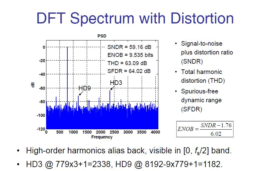
45 Sampling Operation: Nyquist Rate According to the sampling theorem: If no alias issues, then Ideal sampling does not add distortion but replicas of the original spectrum
46 Signal Sampling Theorem Time domain sampling Frequency Spectrum
47 Signal Sampling employing a train of pulses Time domain sampling with pulses Spectrum


48 Alias issue if undersampling
49
50 Under-sampling of a broadband signal
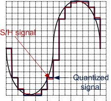
51 S/H and Quantization errors The sampling and Held operations generate alias frequency components and (sinc) signal distortion, respectively Error is an odd function (no even harmonic distortions, why?) Quantization generates harmonic distortion components when sinusoidal input signals are used S ( t) = S ( t) Error( t) in q + Error signal Quantized signal Freq Freq
52 Distortion due to quantization errors
53 ADC metrics: Quantization error Signal is sampled at given instants Signal is encoded to a limited number of codes resulting in quantization noise (random signals) and distortion (periodic signals)
54
55 What the fundamental problem is? Mapping an infinite resolution analog signal into a digital but finite resolution representation
56 Quantization noise for Random (Ramp) input signal
57
58 ADC metrics: SQNR The maximum Signal-to-Quantization Noise ratio (SQNR) for an N-bit ADC: SQNR P A P / 2 ( N / ) db 2 signal ideal = = Pnoise noise = 2 / 12 = 6. 02N For an ADC with a measured SNDR, the effective number of bits is defined as: ENOB = SNDR(dB)
59 Quantization noise density The dynamic range of a system is equal to the signal to noise ratio measured over a bandwidth equal to half of the sampling (Nyquist) frequency Then, σ 2 = 2 q 12 Is the total while the quantization noise density (quantization noise measured in a bandwidth of 1 Hz) Noise density = 2σ f s 2 = 2 q 6f s -fs/2 fs/2

60

61 Incommensurate f s and f in Sampling frequency f s is fixed. Input frequency f in is chosen to satisfy (a) integer number of cycles C and (b) N / C = f s / f in is incommensurate. An easy way is to make N a power of 2 and C a prime number. Additionally to guarantee that the input frequency falls on a DFT freq. bin use f in = f s /2-kf s /N, where k is an integer. Then check inconmesurate requirement. Windowing lifts the need to have an integer number of cycles. Good for measurements. Pick N depending on noise floor requirements: The DFT noise floor is 10*log10(N/2) below the noise floor. Then DFT noise floor = -SNR_ 0dFS -10*log10(N/2).
62
63
64 Practical Limitations
65 Digital to Analog Converters
66 Practical Definitions
67 Practical Limitations
68 Practical Limitations Quite critical issue! Usually not a major issue
69 Practical Limitations: Offset error
70 Practical Limitations Usually not a major issue Quite critical issue!
71 Practical Limitations: Gain error
72 Practical Limitations: Differential Error
73 Practical Limitations
74 Practical Limitations: Integral error
75 Practical Limitations
76 Practical Limitations: Absolute Accuracy
77 Analog to Digital Converters Usually the effects of the systematic offsets can be minimized through calibration or accounted in digital domain
78 Digital to Analog Converters
79 Practical Limitations
80 Practical Limitations
81 Practical Limitations DNL must be smaller or equal to 1 LSB
82 Practical Limitations

83 Offset Voltages
84 Practical Limitations
85
86
87
88
89
FUNDAMENTALS OF ANALOG TO DIGITAL CONVERTERS: PART I.1
 FUNDAMENTALS OF ANALOG TO DIGITAL CONVERTERS: PART I.1 Many of these slides were provided by Dr. Sebastian Hoyos January 2019 Texas A&M University 1 Spring, 2019 Outline Fundamentals of Analog-to-Digital
New RF-to-Digital Architectures for Broadband Communication Systems
 New RF-to-Digital Architectures for Broadband Communication Systems Department of ECE, Texas A&M University Barcelona, May 2012 Barcelona -1- May 2012 Outline Introduction Multi-standard receivers: Front-End
CMOS Analog to Digital Converters : State-of-the-Art and Perspectives in Digital Communications ADC
 CMOS Analog to Digital Converters : State-of-the-Art and Perspectives in Digital Communications ADC Hussein Fakhoury and Hervé Petit C²S Research Group Presentation Outline Introduction Basic concepts
EE247 Lecture 22. Figures of merit (FOM) and trends for ADCs How to use/not use FOM. EECS 247 Lecture 22: Data Converters 2004 H. K.
 and trends for ADCs How to use/not use FOM. EECS 247 Lecture 22: Data Converters 2004 H. K.") EE247 Lecture 22 Pipelined ADCs Combining the bits Stage implementation Circuits Noise budgeting Figures of merit (FOM) and trends for ADCs How to use/not use FOM Oversampled ADCs EECS 247 Lecture 22:
EE247 Lecture 22 Pipelined ADCs Combining the bits Stage implementation Circuits Noise budgeting Figures of merit (FOM) and trends for ADCs How to use/not use FOM Oversampled ADCs EECS 247 Lecture 22:
A 1MHz-64MHz Active RC TI-LPF with Variable Gain for SDR Receiver in 65-nm CMOS
 2017 5th International Conference on Computer, Automation and Power Electronics (CAPE 2017) A 1MHz-64MHz Active RC TI-LPF with Variable Gain for SDR Receiver in 65-nm CMOS Chaoxuan Zhang1, a, *, Xunping
Proposing. An Interpolated Pipeline ADC
 Proposing An Interpolated Pipeline ADC Akira Matsuzawa Tokyo Institute of Technology, Japan Matsuzawa & Okada Lab. Background 38GHz long range mm-wave system Role of long range mm-wave Current Optical
Fundamentals of Data Converters. DAVID KRESS Director of Technical Marketing
 Fundamentals of Data Converters DAVID KRESS Director of Technical Marketing 9/14/2016 Analog to Electronic Signal Processing Sensor (INPUT) Amp Converter Digital Processor Actuator (OUTPUT) Amp Converter
Cascaded Noise-Shaping Modulators for Oversampled Data Conversion
 Cascaded Noise-Shaping Modulators for Oversampled Data Conversion Bruce A. Wooley Stanford University B. Wooley, Stanford, 2004 1 Outline Oversampling modulators for A/D conversion Cascaded noise-shaping
Pipeline vs. Sigma Delta ADC for Communications Applications
 Pipeline vs. Sigma Delta ADC for Communications Applications Noel O Riordan, Mixed-Signal IP Group, S3 Semiconductors noel.oriordan@s3group.com Introduction The Analog-to-Digital Converter (ADC) is a key
Analog to Digital Conversion
 Analog to Digital Conversion Florian Erdinger Lehrstuhl für Schaltungstechnik und Simulation Technische Informatik der Uni Heidelberg VLSI Design - Mixed Mode Simulation F. Erdinger, ZITI, Uni Heidelberg
Design of a High-speed, High-resolution ADC for Medical Ultrasound Applications -
 The figures of merit (FoMs) encompassing power, effective resolution and speed rank the dynamic performance of the ADC core among the best in its class. J. Bjørnsen: Design of a High-speed, High-resolution
Sigma-Delta ADC Tutorial and Latest Development in 90 nm CMOS for SoC
 Sigma-Delta ADC Tutorial and Latest Development in 90 nm CMOS for SoC Jinseok Koh Wireless Analog Technology Center Texas Instruments Inc. Dallas, TX Outline Fundamentals for ADCs Over-sampling and Noise
Reconfigurable Low-Power Continuous-Time Sigma-Delta Converter for Multi- Standard Applications
 ECEN-60: Mixed-Signal Interfaces Instructor: Sebastian Hoyos ASSIGNMENT 6 Reconfigurable Low-Power Continuous-Time Sigma-Delta Converter for Multi- Standard Applications ) Please use SIMULINK to design
DESIGN OF MULTI-BIT DELTA-SIGMA A/D CONVERTERS
 DESIGN OF MULTI-BIT DELTA-SIGMA A/D CONVERTERS DESIGN OF MULTI-BIT DELTA-SIGMA A/D CONVERTERS by Yves Geerts Alcatel Microelectronics, Belgium Michiel Steyaert KU Leuven, Belgium and Willy Sansen KU Leuven,
Receiver Architecture
 Receiver Architecture Receiver basics Channel selection why not at RF? BPF first or LNA first? Direct digitization of RF signal Receiver architectures Sub-sampling receiver noise problem Heterodyne receiver
EE247 Lecture 23. Advanced calibration techniques. Compensating inter-stage amplifier non-linearity Calibration via parallel & slow ADC
 EE247 Lecture 23 Pipelined ADCs Combining the bits Stage implementation Circuits Noise budgeting Advanced calibration techniques Compensating inter-stage amplifier non-linearity Calibration via parallel
An All CMOS, 2.4 GHz, Fully Adaptive, Scalable, Frequency Hopped Transceiver
 An All CMOS, 2.4 GHz, Fully Adaptive, Scalable, Frequency Hopped Transceiver Farbod Behbahani John Leete Alexandre Kral Shahrzad Tadjpour Karapet Khanoyan Paul J. Chang Hooman Darabi Maryam Rofougaran
Lecture #6: Analog-to-Digital Converter
 Lecture #6: Analog-to-Digital Converter All electrical signals in the real world are analog, and their waveforms are continuous in time. Since most signal processing is done digitally in discrete time,
2. ADC Architectures and CMOS Circuits
 /58 2. Architectures and CMOS Circuits Francesc Serra Graells francesc.serra.graells@uab.cat Departament de Microelectrònica i Sistemes Electrònics Universitat Autònoma de Barcelona paco.serra@imb-cnm.csic.es
Research and Development Activities in RF and Analog IC Design. RFIC Building Blocks. Single-Chip Transceiver Systems (I) Howard Luong
 Howard Luong") Research and Development Activities in RF and Analog IC Design Howard Luong Analog Research Laboratory Department of Electrical and Electronic Engineering Hong Kong University of Science and Technology
Research and Development Activities in RF and Analog IC Design Howard Luong Analog Research Laboratory Department of Electrical and Electronic Engineering Hong Kong University of Science and Technology
Analog-to-Digital Converter Survey & Analysis. Bob Walden. (310) Update: July 16,1999
 Update: July 16,1999") Analog-to-Digital Converter Survey & Analysis Update: July 16,1999 References: 1. R.H. Walden, Analog-to-digital converter survey and analysis, IEEE Journal on Selected Areas in Communications, vol. 17,
Analog-to-Digital Converter Survey & Analysis Update: July 16,1999 References: 1. R.H. Walden, Analog-to-digital converter survey and analysis, IEEE Journal on Selected Areas in Communications, vol. 17,
NPTEL. VLSI Data Conversion Circuits - Video course. Electronics & Communication Engineering.
 NPTEL Syllabus VLSI Data Conversion Circuits - Video course COURSE OUTLINE This course covers the analysis and design of CMOS Analog-to-Digital and Digital-to-Analog Converters,with about 7 design assigments.
A 12-bit Interpolated Pipeline ADC using Body Voltage Controlled Amplifier
 A 12-bit Interpolated Pipeline ADC using Body Voltage Controlled Amplifier Hyunui Lee, Masaya Miyahara, and Akira Matsuzawa Tokyo Institute of Technology, Japan Outline Background Body voltage controlled
Design of Continuous Time Multibit Sigma Delta ADC for Next Generation Wireless Applications
 RESEARCH ARTICLE OPEN ACCESS Design of Continuous Time Multibit Sigma Delta ADC for Next Generation Wireless Applications Sharon Theresa George*, J. Mangaiyarkarasi** *(Department of Information and Communication
Architectures and circuits for timeinterleaved. Sandeep Gupta Teranetics, Santa Clara, CA
 Architectures and circuits for timeinterleaved ADC s Sandeep Gupta Teranetics, Santa Clara, CA Outline Introduction to time-interleaved architectures. Conventional Sampling architectures and their application
Integrated Microsystems Laboratory. Franco Maloberti
 University of Pavia Integrated Microsystems Laboratory Power Efficient Data Convertes Franco Maloberti franco.maloberti@unipv.it OUTLINE Introduction Managing the noise power budget Challenges of State-of-the-art
A 1.9GHz Single-Chip CMOS PHS Cellphone
 A 1.9GHz Single-Chip CMOS PHS Cellphone IEEE JSSC, Vol. 41, No.12, December 2006 William Si, Srenik Mehta, Hirad Samavati, Manolis Terrovitis, Michael Mack, Keith Onodera, Steve Jen, Susan Luschas, Justin
A 130mW 100MS/s Pipelined ADC with 69dB SNDR Enabled by Digital Harmonic Distortion Correction. Andrea Panigada, Ian Galton
 A 130mW 100MS/s Pipelined ADC with 69dB SNDR Enabled by Digital Harmonic Distortion Correction Andrea Panigada, Ian Galton University of California at San Diego, La Jolla, CA INTEGRATED SIGNAL PROCESSING
A 60-dB Image Rejection Filter Using Δ-Σ Modulation and Frequency Shifting
 A 60-dB Image Rejection Filter Using Δ-Σ Modulation and Frequency Shifting Toshihiro Konishi, Koh Tsuruda, Shintaro Izumi, Hyeokjong Lee, Hidehiro Fujiwara, Takashi Takeuchi, Hiroshi Kawaguchi, and Masahiko
Asynchronous SAR ADC: Past, Present and Beyond. Mike Shuo-Wei Chen University of Southern California MWSCAS 2014
 Asynchronous SAR ADC: Past, Present and Beyond Mike Shuo-Wei Chen University of Southern California MWSCAS 2014 1 Roles of ADCs Responsibility of ADC is increasing more BW, more dynamic range Potentially
A SWITCHED-CAPACITOR POWER AMPLIFIER FOR EER/POLAR TRANSMITTERS
 A SWITCHED-CAPACITOR POWER AMPLIFIER FOR EER/POLAR TRANSMITTERS Sang-Min Yoo, Jeffrey Walling, Eum Chan Woo, David Allstot University of Washington, Seattle, WA Submission Highlight A fully-integrated
Wideband Direct Digital Radio Modeling and Verification Rulon VanDyke 1, David Leiss 2
 IMS2011 Wideband Direct Digital Radio Modeling and Verification Rulon VanDyke 1, David Leiss 2 1 Agilent Technologies, Alpharetta, GA, USA 2 Agilent Technologies, Manassas, VA, USA Typical Presentation
Research on Flexible radios. Dr. Krishnamurthy Soumyanath Intel Fellow Director, Communications Circuits Lab
 Research on Flexible radios Dr. Krishnamurthy Soumyanath Intel Fellow Director, Communications Circuits Lab Tomorrow s needs Today 2008-10 2010+ WLAN WLAN WWAN WPAN WLAN WWAN WWAN Discrete Radios One/multi
Summary Last Lecture
 Interleaved ADCs EE47 Lecture 4 Oversampled ADCs Why oversampling? Pulse-count modulation Sigma-delta modulation 1-Bit quantization Quantization error (noise) spectrum SQNR analysis Limit cycle oscillations
Appendix A Comparison of ADC Architectures
 Appendix A Comparison of ADC Architectures A comparison of continuous-time delta-sigma (CT ), pipeline, and timeinterleaved (TI) SAR ADCs which target wide signal bandwidths (greater than 100 MHz) and
1 Introduction to Highly Integrated and Tunable RF Receiver Front Ends
 1 Introduction to Highly Integrated and Tunable RF Receiver Front Ends 1.1 Introduction With the ever-increasing demand for instant access to data over wideband communication channels, the quest for a
Summary Last Lecture
 EE47 Lecture 5 Pipelined ADCs (continued) How many bits per stage? Algorithmic ADCs utilizing pipeline structure Advanced background calibration techniques Oversampled ADCs Why oversampling? Pulse-count
Low-Power Decimation Filter Design for Multi-Standard Transceiver Applications
 i Low-Power Decimation Filter Design for Multi-Standard Transceiver Applications by Carol J. Barrett Master of Science in Electrical Engineering University of California, Berkeley Professor Paul R. Gray,
Radio Research Directions. Behzad Razavi Communication Circuits Laboratory Electrical Engineering Department University of California, Los Angeles
 Radio Research Directions Behzad Razavi Communication Circuits Laboratory Electrical Engineering Department University of California, Los Angeles Outline Introduction Millimeter-Wave Transceivers - Applications
DESIGN OF A 500MHZ, 4-BIT LOW POWER ADC FOR UWB APPLICATION
 DESIGN OF A 500MHZ, 4-BIT LOW POWER ADC FOR UWB APPLICATION SANTOSH KUMAR PATNAIK 1, DR. SWAPNA BANERJEE 2 1,2 E & ECE Department, Indian Institute of Technology, Kharagpur, Kharagpur, India Abstract-This
IF-Sampling Digital Beamforming with Bit-Stream Processing. Jaehun Jeong
 IF-Sampling Digital Beamforming with Bit-Stream Processing by Jaehun Jeong A dissertation submitted in partial fulfillment of the requirements for the degree of Doctor of Philosophy (Electrical Engineering)
2.4 A/D Converter Survey Linearity
 2.4 A/D Converter Survey 21 mum and minimum power spectral density (PSD) levels. In the case of a single-channel receiver, this implies the gain control range of the VGA, while in a multi-channel receiver
ECE 6560 Multirate Signal Processing Chapter 13
 Multirate Signal Processing Chapter 13 Dr. Bradley J. Bazuin Western Michigan University College of Engineering and Applied Sciences Department of Electrical and Computer Engineering 1903 W. Michigan Ave.
A K-Delta-1-Sigma Modulator for Wideband Analog-to-Digital Conversion
 A K-Delta-1-Sigma Modulator for Wideband Analog-to-Digital Conversion Abstract : R. Jacob Baker and Vishal Saxena Department of Electrical and Computer Engineering Boise State University jbaker@boisestate.edu
Music 270a: Fundamentals of Digital Audio and Discrete-Time Signals
 Music 270a: Fundamentals of Digital Audio and Discrete-Time Signals Tamara Smyth, trsmyth@ucsd.edu Department of Music, University of California, San Diego October 3, 2016 1 Continuous vs. Discrete signals
Another way to implement a folding ADC
 Another way to implement a folding ADC J. Van Valburg and R. van de Plassche, An 8-b 650 MHz Folding ADC, IEEE JSSC, vol 27, #12, pp. 1662-6, Dec 1992 Coupled Differential Pair J. Van Valburg and R. van
A 1.7-to-2.2GHz Full-Duplex Transceiver System with >50dB Self-Interference Cancellation over 42MHz Bandwidth
 A 1.7-to-2.2GHz Full-Duplex Transceiver System with >50dB Self-Interference Cancellation Tong Zhang, Ali Najafi, Chenxin Su, Jacques C. Rudell University of Washington, Seattle Feb. 8, 2017 International
3. DAC Architectures and CMOS Circuits
 1/30 3. DAC Architectures and CMOS Circuits Francesc Serra Graells francesc.serra.graells@uab.cat Departament de Microelectrònica i Sistemes Electrònics Universitat Autònoma de Barcelona paco.serra@imb-cnm.csic.es
BANDPASS delta sigma ( ) modulators are used to digitize
 modulators are used to digitize") 680 IEEE TRANSACTIONS ON CIRCUITS AND SYSTEMS II: EXPRESS BRIEFS, VOL. 52, NO. 10, OCTOBER 2005 A Time-Delay Jitter-Insensitive Continuous-Time Bandpass 16 Modulator Architecture Anurag Pulincherry, Michael
680 IEEE TRANSACTIONS ON CIRCUITS AND SYSTEMS II: EXPRESS BRIEFS, VOL. 52, NO. 10, OCTOBER 2005 A Time-Delay Jitter-Insensitive Continuous-Time Bandpass 16 Modulator Architecture Anurag Pulincherry, Michael
Advanced Digital Signal Processing Part 2: Digital Processing of Continuous-Time Signals
 Advanced Digital Signal Processing Part 2: Digital Processing of Continuous-Time Signals Gerhard Schmidt Christian-Albrechts-Universität zu Kiel Faculty of Engineering Institute of Electrical Engineering
ISSCC 2003 / SESSION 20 / WIRELESS LOCAL AREA NETWORKING / PAPER 20.5
 ISSCC 2003 / SESSION 20 / WIRELESS LOCAL AREA NETWORKING / PAPER 20.5 20.5 A 2.4GHz CMOS Transceiver and Baseband Processor Chipset for 802.11b Wireless LAN Application George Chien, Weishi Feng, Yungping
Wideband Sampling by Decimation in Frequency
 Wideband Sampling by Decimation in Frequency Martin Snelgrove http://www.kapik.com 192 Spadina Ave. Suite 218 Toronto, Ontario, M5T2C2 Canada Copyright Kapik Integration 2011 WSG: New Architectures for
Lecture 9, ANIK. Data converters 1
 Lecture 9, ANIK Data converters 1 What did we do last time? Noise and distortion Understanding the simplest circuit noise Understanding some of the sources of distortion 502 of 530 What will we do today?
Low-Power Pipelined ADC Design for Wireless LANs
 Low-Power Pipelined ADC Design for Wireless LANs J. Arias, D. Bisbal, J. San Pablo, L. Quintanilla, L. Enriquez, J. Vicente, J. Barbolla Dept. de Electricidad y Electrónica, E.T.S.I. de Telecomunicación,
A Low Power 900MHz Superheterodyne Compressive Sensing Receiver for Sparse Frequency Signal Detection
 A Low Power 900MHz Superheterodyne Compressive Sensing Receiver for Sparse Frequency Signal Detection Hamid Nejati and Mahmood Barangi 4/14/2010 Outline Introduction System level block diagram Compressive
A single-slope 80MS/s ADC using two-step time-to-digital conversion
 A single-slope 80MS/s ADC using two-step time-to-digital conversion The MIT Faculty has made this article openly available. Please share how this access benefits you. Your story matters. Citation As Published
PAR4CR: THE DEVELOPMENT OF A NEW SDR-BASED PLATFORM TOWARDS COGNITIVE RADIO
 PAR4CR: THE DEVELOPMENT OF A NEW SDR-BASED PLATFORM TOWARDS COGNITIVE RADIO Olga Zlydareva Co-authors: Martha Suarez Rob Mestrom Fabian Riviere Outline 1 Introduction System Requirements Methodology System
Chapter 2: Digitization of Sound
 Chapter 2: Digitization of Sound Acoustics pressure waves are converted to electrical signals by use of a microphone. The output signal from the microphone is an analog signal, i.e., a continuous-valued
Guest Editorial of Special Issue on Software Defined Radio Transceivers and Circuits for 5G Wireless Communications
 IEEE Transactions on Circuits and Systems-II Guest Editorial of Special Issue on Software Defined Radio Transceivers and Circuits for 5G Wireless Communications W ireless communications is one of the fastest
Analog and Telecommunication Electronics
 Politecnico di Torino Electronic Eng. Master Degree Analog and Telecommunication Electronics D1 - A/D/A conversion systems» Sampling, spectrum aliasing» Quantization error» SNRq vs signal type and level»
Architectures and Design Methodologies for Very Low Power and Power Effective A/D Sigma-Delta Converters
 0 Architectures and Design Methodologies for Very Low Power and Power Effective A/D Sigma-Delta Converters F. Maloberti University of Pavia - Italy franco.maloberti@unipv.it 1 Introduction Summary Sigma-Delta
The Fundamentals of Mixed Signal Testing
 The Fundamentals of Mixed Signal Testing Course Information The Fundamentals of Mixed Signal Testing course is designed to provide the foundation of knowledge that is required for testing modern mixed
Keywords: GPS, receiver, GPS receiver, MAX2769, 2769, 1575MHz, Integrated GPS Receiver, Global Positioning System
 Maxim > Design Support > Technical Documents > User Guides > APP 3910 Keywords: GPS, receiver, GPS receiver, MAX2769, 2769, 1575MHz, Integrated GPS Receiver, Global Positioning System USER GUIDE 3910 User's
mmw to THz ultra high data rate radio access technologies
 mmw to THz ultra high data rate radio access technologies Dr. Laurent HERAULT VP Europe, CEA LETI Pierre Vincent Head of RF IC design Lab, CEA LETI Outline mmw communication use cases and standards mmw
Telecommunication Electronics
 Politecnico di Torino ICT School Telecommunication Electronics C5 - Special A/D converters» Logarithmic conversion» Approximation, A and µ laws» Differential converters» Oversampling, noise shaping Logarithmic
Analog-to-Digital Converters
 EE47 Lecture 3 Oversampled ADCs Why oversampling? Pulse-count modulation Sigma-delta modulation 1-Bit quantization Quantization error (noise) spectrum SQNR analysis Limit cycle oscillations nd order ΣΔ
Challenges in Designing CMOS Wireless System-on-a-chip
 Challenges in Designing CMOS Wireless System-on-a-chip David Su Atheros Communications Santa Clara, California IEEE Fort Collins, March 2008 Introduction Outline Analog/RF: CMOS Transceiver Building Blocks
Session 3. CMOS RF IC Design Principles
 Session 3 CMOS RF IC Design Principles Session Delivered by: D. Varun 1 Session Topics Standards RF wireless communications Multi standard RF transceivers RF front end architectures Frequency down conversion
Lecture 10, ANIK. Data converters 2
 Lecture, ANIK Data converters 2 What did we do last time? Data converter fundamentals Quantization noise Signal-to-noise ratio ADC and DAC architectures Overview, since literature is more useful explaining
Converters Basic Theory and Definitions. Definitions/terms- SNR, ENOBs, DNL, INL.. And Sampling theory..
 Welcome to 046188 Winter semester 2013 Mixed Signal Electronic Circuits Instructor: Dr. M. Moyal Lecture 02 and 03. Converters Basic Theory and Definitions Definitions/terms- SNR, ENOBs, DNL, INL.. And
APPLICATION NOTE 3942 Optimize the Buffer Amplifier/ADC Connection
 Maxim > Design Support > Technical Documents > Application Notes > Communications Circuits > APP 3942 Maxim > Design Support > Technical Documents > Application Notes > High-Speed Interconnect > APP 3942
Multirate DSP, part 3: ADC oversampling
 Multirate DSP, part 3: ADC oversampling Li Tan - May 04, 2008 Order this book today at www.elsevierdirect.com or by calling 1-800-545-2522 and receive an additional 20% discount. Use promotion code 92562
Analog and Telecommunication Electronics
 Politecnico di Torino - ICT School Analog and Telecommunication Electronics D5 - Special A/D converters» Differential converters» Oversampling, noise shaping» Logarithmic conversion» Approximation, A and
SAMPLING FREQUENCY SELECTION SCHEME FOR A MULTIPLE SIGNAL RECEIVER USING UNDERSAMPLING
 SAMPLING FREQUENCY SELECTION SCHEME FOR A MULTIPLE SIGNAL RECEIVER USING UNDERSAMPLING Yoshio Kunisawa (KDDI R&D Laboratories, yokosuka, kanagawa, JAPAN; kuni@kddilabs.jp) ABSTRACT A multi-mode terminal
A 12b 50MS/s 2.1mW SAR ADC with redundancy and digital background calibration
 A b 5MS/s.mW SAR ADC with redundancy and digital background calibration The MIT Faculty has made this article openly available. Please share how this access benefits you. Your story matters. Citation As
TSEK38: Radio Frequency Transceiver Design Lecture 3: Superheterodyne TRX design
 TSEK38: Radio Frequency Transceiver Design Lecture 3: Superheterodyne TRX design Ted Johansson, ISY ted.johansson@liu.se 2 Outline of lecture 3 Introduction RF TRX architectures (3) Superheterodyne architecture
A 25MS/s 14b 200mW Σ Modulator in 0.18µm CMOS
 UT Mixed-Signal/RF Integrated Circuits Seminar Series A 25MS/s 14b 200mW Σ Modulator in 0.18µm CMOS Pio Balmelli April 19 th, Austin TX 2 Outline VDSL specifications Σ A/D converter features Broadband
ANALYSIS, DESIGN AND IMPLEMENTATION OF NOISE SHAPING DATA CONVERTERS FOR POWER SYSTEMS
 ANALYSIS, DESIGN AND IMPLEMENTATION OF NOISE SHAPING DATA CONVERTERS FOR POWER SYSTEMS Maraim Asif 1, Prof Pallavi Bondriya 2 1 Department of Electrical and Electronics Engineering, Technocrats institute
Lab.3. Tutorial : (draft) Introduction to CODECs
 Introduction to CODECs") Lab.3. Tutorial : (draft) Introduction to CODECs Fig. Basic digital signal processing system Definition A codec is a device or computer program capable of encoding or decoding a digital data stream or
Lab.3. Tutorial : (draft) Introduction to CODECs Fig. Basic digital signal processing system Definition A codec is a device or computer program capable of encoding or decoding a digital data stream or
Oversampling Converters
 Oversampling Converters Behzad Razavi Electrical Engineering Department University of California, Los Angeles Outline Basic Concepts First- and Second-Order Loops Effect of Circuit Nonidealities Cascaded
ISSCC 2004 / SESSION 25 / HIGH-RESOLUTION NYQUIST ADCs / 25.4
 ISSCC 2004 / SESSION 25 / HIGH-RESOLUTION NYQUIST ADCs / 25.4 25.4 A 1.8V 14b 10MS/s Pipelined ADC in 0.18µm CMOS with 99dB SFDR Yun Chiu, Paul R. Gray, Borivoje Nikolic University of California, Berkeley,
A 4 GSample/s 8-bit ADC in. Ken Poulton, Robert Neff, Art Muto, Wei Liu, Andrew Burstein*, Mehrdad Heshami* Agilent Laboratories Palo Alto, California
 A 4 GSample/s 8-bit ADC in 0.35 µm CMOS Ken Poulton, Robert Neff, Art Muto, Wei Liu, Andrew Burstein*, Mehrdad Heshami* Agilent Laboratories Palo Alto, California 1 Outline Background Chip Architecture
AD9772A - Functional Block Diagram
 F FEATURES single 3.0 V to 3.6 V supply 14-Bit DAC Resolution 160 MPS Input Data Rate 67.5 MHz Reconstruction Passband @ 160 MPS 74 dbc FDR @ 25 MHz 2 Interpolation Filter with High- or Low-Pass Response
Cascaded Noise Shaping for Oversampling A/D and D/A Conversion Bruce A. Wooley Stanford University
 Cascaded Noise Shaping for Oversampling A/D and D/A Conversion Bruce A. Wooley Stanford University Bruce A. Wooley - 1 - Copyright 2005, Stanford University Outline Oversampling modulators for A-to-D conversion
II Year (04 Semester) EE6403 Discrete Time Systems and Signal Processing
 EE6403 Discrete Time Systems and Signal Processing") Class Subject Code Subject II Year (04 Semester) EE6403 Discrete Time Systems and Signal Processing 1.CONTENT LIST: Introduction to Unit I - Signals and Systems 2. SKILLS ADDRESSED: Listening 3. OBJECTIVE
Class Subject Code Subject II Year (04 Semester) EE6403 Discrete Time Systems and Signal Processing 1.CONTENT LIST: Introduction to Unit I - Signals and Systems 2. SKILLS ADDRESSED: Listening 3. OBJECTIVE
A 35 fj 10b 160 MS/s Pipelined- SAR ADC with Decoupled Flip- Around MDAC and Self- Embedded Offset Cancellation
 Y. Zu, C.- H. Chan, S.- W. Sin, S.- P. U, R.P. Martins, F. Maloberti: "A 35 fj 10b 160 MS/s Pipelined-SAR ADC with Decoupled Flip-Around MDAC and Self- Embedded Offset Cancellation"; IEEE Asian Solid-
MITOPENCOURSEWARE High-Speed Communication Circuits and Systems Lecture 29 Lowpass and Bandpass Delta-Sigma Modulation.
 MITOPENCOURSEWARE MASSACUSETTS INSTITUTE OF TECHNOLOGY 6.976 High-Speed Communication Circuits and Systems Lecture 29 Lowpass and Bandpass Delta-Sigma Modulation Richard Schreier ANALOG DEVICES Copyright
Design of 28 nm FD-SOI CMOS 800 MS/s SAR ADC for wireless applications
 Design of 28 nm FD-SOI CMOS 800 MS/s SAR ADC for wireless applications Master s thesis in Embedded Electronic System Design VICTOR ÅBERG Department of Computer Science and Engineering CHALMERS UNIVERSITY
Power Reduction in RF
 Power Reduction in RF SoC Architecture using MEMS Eric Mercier 1 RF domain overview Technologies Piezoelectric materials Acoustic systems Ferroelectric materials Meta materials Magnetic materials RF MEMS
BER-optimal ADC for Serial Links
 BER-optimal ADC for Serial Links Speaker Name: Yingyan Lin Co-authors: Min-Sun Keel, Adam Faust, Aolin Xu, Naresh R. Shanbhag, Elyse Rosenbaum, and Andrew Singer Advisor s name: Naresh R. Shanbhag Affiliation:
Flexible CMOS Frequency Translation Circuits
 Flexible CMOS Frequency Translation Circuits Eric Klumperink Zhiyu Ru, Michiel Soer, Bram Nauta 1 Outline Intro Analog Front Ends for SDR Interferer robust SDR Receiver analog part Interferer robust SDR
SiNANO-NEREID Workshop:
 SiNANO-NEREID Workshop: Towards a new NanoElectronics Roadmap for Europe Leuven, September 11 th, 2017 WP3/Task 3.2 Connectivity RF and mmw Design Outline Connectivity, what connectivity? High data rates
Pulse-Based Ultra-Wideband Transmitters for Digital Communication
 Pulse-Based Ultra-Wideband Transmitters for Digital Communication Ph.D. Thesis Defense David Wentzloff Thesis Committee: Prof. Anantha Chandrakasan (Advisor) Prof. Joel Dawson Prof. Charles Sodini Ultra-Wideband
INTEGRATED CIRCUIT BLOCKS FOR HIGH PERFORMANCE BASEBAND AND RF ANALOG-TO-DIGITAL CONVERTERS
 INTEGRATED CIRCUIT BLOCKS FOR HIGH PERFORMANCE BASEBAND AND RF ANALOG-TO-DIGITAL CONVERTERS A Thesis by HONGBO CHEN Submitted to the Office of Graduate Studies of Texas A&M University in partial fulfillment
Electronics A/D and D/A converters
 Electronics A/D and D/A converters Prof. Márta Rencz, Gábor Takács, Dr. György Bognár, Dr. Péter G. Szabó BME DED December 1, 2014 1 / 26 Introduction The world is analog, signal processing nowadays is
The Case for Oversampling
 EE47 Lecture 4 Oversampled ADCs Why oversampling? Pulse-count modulation Sigma-delta modulation 1-Bit quantization Quantization error (noise) spectrum SQNR analysis Limit cycle oscillations nd order ΣΔ
DIGITAL FILTERING OF MULTIPLE ANALOG CHANNELS
 DIGITAL FILTERING OF MULTIPLE ANALOG CHANNELS Item Type text; Proceedings Authors Hicks, William T. Publisher International Foundation for Telemetering Journal International Telemetering Conference Proceedings
Lecture Schedule: Week Date Lecture Title
 http://elec3004.org Sampling & More 2014 School of Information Technology and Electrical Engineering at The University of Queensland Lecture Schedule: Week Date Lecture Title 1 2-Mar Introduction 3-Mar
Testing A/D Converters A Practical Approach
 Testing A/D Converters A Practical Approach Mixed Signal The seminar entitled Testing Analog-to-Digital Converters A Practical Approach is a one-day information intensive course, designed to address the
BandPass Sigma-Delta Modulator for wideband IF signals
 BandPass Sigma-Delta Modulator for wideband IF signals Luca Daniel (University of California, Berkeley) Marco Sabatini (STMicroelectronics Berkeley Labs) maintain the same advantages of BaseBand converters