Flexible CMOS Frequency Translation Circuits
|
|
|
- Randolph Harrison
- 5 years ago
- Views:
Transcription
1 Flexible CMOS Frequency Translation Circuits Eric Klumperink Zhiyu Ru, Michiel Soer, Bram Nauta 1
2 Outline Intro Analog Front Ends for SDR Interferer robust SDR Receiver analog part Interferer robust SDR Receiver digital part Mixing or Sampling? Mixer-first Receiver N-path Circuit Generalization Conclusion 2
3 Analog Front-End Interference strong: filtering Signal weak: amplification Frequency high: downconversion ADC speed and resolution are relaxed Channel-filter has better selectivity in baseband 3
4 Analog Front End Challenges Wanted for Software Defined Radio: Compatible with digital Flexible RF-frequency: wideband receiver with good NF Flexible channel-selection filtering: tunable LPF Be robust to in-band interference (often not so strong) Be robust to out-of-band interference: can be huge Wideband receiver wideband interference 4
5 Solutions: what has been proposed? International Solid-State Circuits Conference (ISSCC) 5
![UCLA SDR Receiver [Bagheri, ISSCC06, UCLA] Wideband receiver: demonstrated at 800MHz & 2.](/docs-images/95/125505010/images/6-0.jpg "4GHz Wideband CG-CS Balun-LNA (noise cancelling) Passive mixer Tunable baseband discrete-time filter Claim: no")
6 UCLA SDR Receiver [Bagheri, ISSCC06, UCLA] Wideband receiver: demonstrated at 800MHz & 2.4GHz Wideband CG-CS Balun-LNA (noise cancelling) Passive mixer Tunable baseband discrete-time filter Claim: no RF-filter needed, but room for doubts. 6

7 UCLA SDR Receiver: BB filter Tunable baseband filter with sufficient attenuation to support different standards, e.g. GSM WiFi (801.11g) 7
![IMEC SDR Receiver 1 [Giannini, ISSCC09, IMEC] On-chip balun makes antenna interface simpler Two LNAs: to address both 1/f noise and high](/docs-images/95/125505010/images/8-0.jpg "frequency Passive mixer for good linearity and 1/f noise Continuous-time tunable BB filter Rely on external filter for Out-of-Band")
8 IMEC SDR Receiver 1 [Giannini, ISSCC09, IMEC] On-chip balun makes antenna interface simpler Two LNAs: to address both 1/f noise and high frequency Passive mixer for good linearity and 1/f noise Continuous-time tunable BB filter Rely on external filter for Out-of-Band Interference 8
![Skyworks Multiband Transceiver [Pullela, ISSCC09, Skyworks] only receiver part shown here Multiband transceiver for GSM:](/docs-images/95/125505010/images/9-0.jpg "850/900/1800/1900MHz Share I/Q mixer & baseband Does not continuously cover bandwidth Not integrated: SAW filters, PAs and")
9 Skyworks Multiband Transceiver [Pullela, ISSCC09, Skyworks] only receiver part shown here Multiband transceiver for GSM: 850/900/1800/1900MHz Share I/Q mixer & baseband Does not continuously cover bandwidth Not integrated: SAW filters, PAs and duplexers 9
![IMEC SDR Receiver 2 [Ingels, ISSCC10, IMEC] In practice, multi-band](/docs-images/95/125505010/images/10-0.jpg "antenna is a challenge, so LNA bank is a reasonable solution for")

10 IMEC SDR Receiver 2 [Ingels, ISSCC10, IMEC] In practice, multi-band antenna is a challenge, so LNA bank is a reasonable solution for short-term Similar to commercial multi-band receivers, but continuously covers a wide RF band Still each standard needs an external SAW filter 10
11 Outline Intro Analog Front Ends for SDR Interferer robust SDR Receiver analog part Interferer robust SDR Receiver digital part Mixing or Sampling? Mixer-first Receiver N-path Circuit Generalization Conclusion 11
12 A Software-Defined Radio Receiver Architecture Robust to Out-of-Band Interference [Ru, ISSCC 2009, JSSC2009] 12
13 Wideband Interference: Nonlinearity Wideband LNA: also amplifies interference nonlinearity 13
14 Wideband Interference: Harmonic Mixing Switching mixer: square-wave LO harmonic mixing 14
15 Low Noise Transconductance at RF V-I instead of voltage gain at RF I-V together/after low-pass filter (LPF) to reduce blockers Keep low impedance over a wide band at node B 15
16 Realization: Wideband LNTA + Mixer + TIA LNTA: high G m & high R out low noise small voltage swing at node B good linearity Similar to [1], but now wideband and with blocker filtering [1] Redman-White & Leenaerts, ESSCIRC07 16
17 Harmonic Rejection (HR) Mixer: Remove 3LO and 5LO rd th cancel! Amplitude weighting + phase shifting emulate sine-lo [2] Weldon et. al., ISSCC01 17
18 Problem: Amplitude and Phase Errors 3 rd or 5 th harmonic vector diagram Amplitude and phase errors unwanted harmonic residue degrade HR ratio How to make irrational ratio, e.g. 2, on chip? 18
19 2-Stage Polyphase HR: Concept 41/29=1.4138, 2= ε=0.03% 19
20 2-Stage Polyphase HR: Realization 50Ω 2G m Ω 3G m G m RF LNTA for 1 st -stage weighting (2:3:2) BB resistor for 2 nd -stage weighting (5:7:5) Nominally 2, what about influence of mismatch? 20
21 Reduced Effect of Amplitude Mismatch 2-stage polyphase product of relative errors E.g. 2:3:2 α=6% 1 st -stage only: HR3=40dB 5:7:5 β=1% 2-stage total: HR3=86dB NOTE: Also an accurate clock is needed (later) 21
22 RF Filtering is Relaxed! Low-pass filtering: attenuates interference around LO 2-stage polyphase HR: robustly attenuates 3LO and 5LO f 22
23 Zero-IF Receiver Prototype 23

24 Chip Photo 1mm 2 in 65nm CMOS VDD: 1.2V Current consumption: Analog 33mA Digital 17mA 24
25 Measured HR: 40 Chips HR 0.8G LO HR Ratio (db) th 3rd Sample # No trimming & calibration, no RF filtering 25
26 Measured Performance Summary +3dBm / +46dBm / LO Frequency 0.4~0.9GHz Gain 34.4±0.2dB DSB NF 4dB±0.5dB S 11 < -10dB 80M~5.5GHz In/Out-of-band IIP dBm In/Out-of-band IIP dBm IF Bandwidth 12MHz 1/f noise 30kHz corner VDD 1.2V Current Consumption Analog: 33mA Digital (clock): 0.4GHz 0.9GHz Harmonic Rejection 0.8GHz LO 3 rd -order > 60dB (40 chips) 5 th -order > 64dB (40 chips) 2 nd, 4 th, 6 th > 62dB (20 chips) 1 Out-of-band IIP3: two tones = 1.61G & 2.40GHz, LO = 819MHz 2 Out-of-band IIP2: two tones = 1.80G & 2.40GHz, LO = 601MHz 26
27 Conclusion: A SDR Receiver Architecture Robust to Out-of-Band Interference Only voltage BB after low-pass filtering Blocking point enhanced by 10dB w.r.t. P 1dB In-band IIP3 +3dBm & out-of-band IIP3 +18dBm 2-stage polyphase harmonic rejection technique Robust: error = product of errors Accurate multiphase clock (discussed later) Minimum HR 60dB (40 chips) - NO calibration/rf filters 27
28 Outline Intro Analog Front Ends for SDR Interferer robust SDR Receiver analog part Interferer robust SDR Receiver digital part Mixing or Sampling? Mixer-first Receiver N-path Circuit Generalization Conclusion 28
29 Digital Assisted approach Harmonic Rejection Exploiting Adaptive Interference Cancellation [Moseley, ISSCC 2009] 29
30 Only first stage of 2-stage HR receiver To Digital Harmonic Rejection Algorithm (Baseband processor) 30
31 The Basic Idea Subtract interference (residual harmonic image responses) from received signal. Need interference estimate signal. 31
32 Adaptive Interference Cancelling (AIC) Adaptive filter aligns phase & amplitude. Minimizes cross-correlation v(n) and e(n). 32
33 Two I/Q signals, 45 degrees rotated Chip ADC 2Gm 50Ω ADC RF + - 3Gm 50Ω ADC 2Gm CLK Ω ADC 33
34 Interference estimate generation Contains unwanted harmonic responses, but desired signal 34
35 AIC Algorithm 1/5 35
36 AIC Algorithm 2/5 36
37 AIC Algorithm 3/5 37
38 AIC Algorithm 4/5 38
39 AIC Algorithm 5/5 39
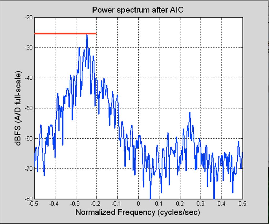
40 Demonstration 40
41 Demonstration 41
42 Demonstration 42
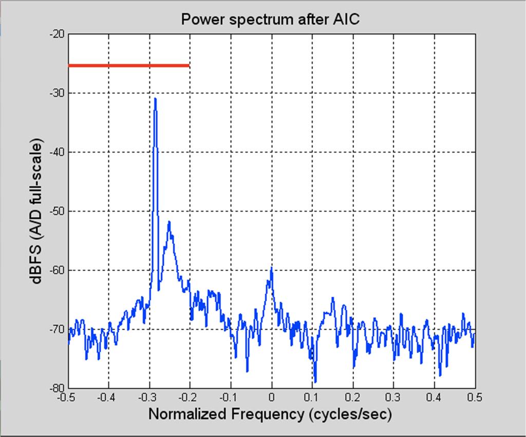
43 Demonstration 43
44 Demonstration: FM signal at 3 rd harmonic 44
45 Comparison This work Z. Ru ISSCC Reject strongest >80 db (1) >60 db Reject the other >36 db >60 db (3 rd or 5 th ) Reject even >64 db >62 db Power frontend V (excl. ADCs) V (excl. ADCs) Power DSP < V N/A (100 Msps) (simulated) # ADCs 4 / 2 if AIC off 2 (1) If one harmonic interference image band is dominating. 45
46 Adaptive Interference Cancellation: Conclusions Dual-domain Harmonic Rejection Mixer (HRM): Analog HRM + 4 ADCs + Digital AIC. Strongest correlating harmonic image is removed X-correlation -> independent of signal shape Stronger interferer -> more rejection Measurements: First stage (analog) HR > 36 db. Dual domain HR3 or HR5 > 80 db. 46
47 Outline Intro Analog Front Ends for SDR Interferer robust SDR Receiver analog part Interferer robust SDR Receiver digital part Mixing or Sampling? Mixer-first Receiver N-path Circuit Generalization Conclusion 47
48 Mixing or Sampling? Is it a mixer or a sampler? 48
49 Frequency Conversion Classification Input Analog-CT Analog-DT Digital Principle Mixing CT Mixing DT Mixing Digital Mixing Sampling CT-to-DT Sampling DT Resampling Digital Resampling CT = Continuous-Time DT = Discrete-Time 49 49
50 Is this Mixing or Sampling? Can be both 50
51 Mixing or Sampling: Use of output? Rate? Use in a CT system Use in a DT system The distinction is NOT in the circuit itself Key question: how is the output signal used?? Does observation rate change or not? CT Mixing: RF(t) IF(t) No CT-to-DT Sampling: RF(t) IF(k) Yes! 51
52 Mixing or Sampling: Classification Input Principle Mixing (observation rate does not change) Sampling (observation rate does change) Analog-CT Analog-DT Digital CT Mixing DT Mixing Digital Mixing CT-to-DT Sampling DT Resampling Digital Resampling Notes: Mixing Output remains Analog-CT, Analog-DT or Digital (=input rate ) Analog is considered as infinite rate Sampling Output rate differs from input, e.g. CT to DT, decimate Sampling may but need not give down-conversion (aliasing) choose via pre-filtering 52
53 Receiver Architectures for SDR (a) CT-Mixing Receiver (b) RF-Sampling Receiver (c) Ideal-Software-Radio Receiver Trend of moving mixer-lpf into digital 53
54 Fit to Three Receiver Architectures Input Analog-CT Analog-DT Digital Principle Mixing (observation rate does not change) Sampling (observation rate does change) CT Mixing 1 DT Mixing Digital Mixing 3 CT-to-DT DT Re- Digital Re- Sampling 2 sampling 2 sampling 3 1 CT-mixing receiver 2 RF-sampling receiver 3 Ideal SWR receiver 54
55 Outline Intro Analog Front Ends for SDR Interferer robust SDR Receiver analog part Interferer robust SDR Receiver digital part Mixing or Sampling? Mixer-first Receiver N-path Circuit Generalization Conclusion 55
56 Mixer-first receiver: A 0.2-to-2.0GHz 65nm CMOS Receiver Without LNA Achieving >11dBm IIP3 and <6.5dB NF [Soer, ISSCC2009] 56
57 Motivation: High Dynamic Range Goal: receiver for Software Defined Radio Spurious Free Dynamic Range (SFDR): Difference between strongest interferer and weakest detectable signal Determines filter requirements Limited both by noise and nonlinearity Assume noise figure NF and bandwidth B Linearity is usually limited by IIP3 Assuming noise and IM3 are equal: 2 SFDR 3 (IIP3 NF 10logB 174dBm) High SFDR low NF, high IIP3 57
58 LNA-first vs. Mixer-first LNA-first: Low noise LNA Feedback RF Moderate LNA linearity active Active-mixer-first: Feedback IF Moderate mixer linearity Noise folding 58
59 Proposed Architecture passive Use passive mixer: High linearity No voltage gain before mixer: Noise folding? Conversion loss? Solve with: Harmonic cancellation Optimized mixer duty cycle 59
60 Mixer Operation RF LO IF -f S 0 f S -f S f S Linear Periodically Time Variant: LO frequency f S 0 -f S 0 f S Convolution with harmonics (not all shown) Noise folding increases NF 60
61 Mixing vs. Sampling Downconversion Pull to zero R 1 R 2 R1 R 2 ½ -4f S -3f S -2f S -f S 0 f S 2f S 3f S 4f S Mixer conversion gain: -9.9dB T ON Hold! T on R C R C ½ -4f S -3f S -2f S -f S 0 f S 2f S 3f S 4f S Sampler conversion gain: -3.9dB 61
62 Multiphase + - Balanced: 180 clock phase difference No RF- and DC feed-through Cancel even-order harmonics I Q In-phase / Quadrature: 90 clock phase difference Image rejection? Clocks overlap! 62
63 25% Quadrature Sampling Mixer (T on <<RC) A B C D A C B D T on I+ I- Q+ Q- R C -0.9dB 0-5f s -4f s -3f s -2f s -f s f s 2f s 3f s 4f s 5f s Balanced I/Q image rejection -0.9dB conversion gain 0.9dB NF 63
64 LPTV circuit Input Impedance Actual use: V S as input R S part of mixer Most power reflected Also moved to other different harmonics, reflected and dissipated in R S V S R S + - source Z IN High input impedance : Weired : f(r s )!! High, but not infinite Input current modulated by switching Duty cycle dependent 25% duty cycle : Z 4.2 IN R S [Cook, ISSCC 2006] 64
65 RF Filter RF Filter needed: Reject 3 rd harmonic and out-of-band interferers Not included in ICdesign 50Ω Design for high Z IN : No standard filter Z 4.2 IN R S 50 Ω Low pass example 210 Ω 65
66 Single-Ended to Differential Total Design Differential Four-phase Clocks Differential 5Ω Switches Feedback Amplifier 66

67 Chip Micrograph 65nm CMOS, active area 0.13mm 2 67
68 25 20 Gain, IIP3 and DSB NF vs. RF Gain [db] NF IIP [dbm] Lines: simulation Markers: measurement RF frequency [MHz] 68
69 Gain, IIP3 and DSB NF vs. IF 25 Gain IIP3 15 [db] [dbm] NF Lines: simulation Markers: measurement IF frequency [MHz] Note: out-of-band IIP3 is even higher ~+25dBm 0 69
70 This Work Benchmarking [Bagheri, ISSCC 2006] [van de Beek, ISSCC 2008] Tektronix RSA2200A RF Frequency GHz IF -3dB Bandwidth ~10 MHz Gain db DSB NF db IIP dbm IIP dbm SFDR in 1MHz BW db Power Dissipation mw Supply Voltage V Active Area < < 0.2 mm 2 Technology 65nm 90nm 45nm CMOS 70
71 Mixer-first receiver: Conclusions Linear mixer-first downconverter Mixing before IF Sampling passive mixer low conversion loss 25% duty cycle image rejection and balancing High SFDR demonstrated Multi-phase harmonic cancelling low NF Passive mixer + feedback amplifier high IIP3 71
72 Outline Intro Analog Front Ends for SDR Interferer robust SDR Receiver analog part Interferer robust SDR Receiver digital part Mixing or Sampling? Mixer-first Receiver N-path Circuit Generalization Conclusion 72
73 Mixer-First Receiver States Single Ended series switch-rc Kernel in each clock-phase 73

74 Polyphase Kernels Shared properties of the circuits: Each Kernel = Switched series-r-c: Activated by Polyphase clocks: S1 S2 S3 Non-overlapping on-time Circuit state Capacitor voltage hold-phase! Output LTV combination of C-voltages 74
75 Outcome: Harmonic Transfer Functions Periodic time variant behaviour gives shape: H -2 (s) H -1 (s) H 0 (s) H 1 (s) H 2 (s) V i (f i ) V o (f o ) 1 e^ j2π n f s t Input signal components get: Filtered Shifted in frequency Added One input component gives multiple output contributions [Ström,CAS1977],[Soer, TCASI, 2010] 75
![Result: Equivalent Model of Kernel-Behaviour [Soer, TCASI, 2010] f s After quite some](/docs-images/95/125505010/images/76-1.jpg "math: G SE (f i ) Models behavior for any value of R, C, D(uty cycle), f i, f s, f o f i")
76 Result: Equivalent Model of Kernel-Behaviour [Soer, TCASI, 2010] f s After quite some math: G SE (f i ) Models behavior for any value of R, C, D(uty cycle), f i, f s, f o f i /f s 76


77 Crucial parameter: Small or Big =t on /RC Both show a hold, but only big tracks and samples input well For small : simplification for 0 and :, 1 Harmonic Mixing including a first-order low-pass filter defined by RC and D Big : Small : 77
78 Mixing and Sampling Region SE kernel noise in [10-17 V 2 /Hz] for f s =100MHz, f o =0Hz, D=1/4 100 C [pf] Sampling Mixing Noise reduction: Sampler: high C Mixer: lower R SE Kernel Noise PSD Mixing Approx. Sampling Approx R [ ] 78
79 Combining Kernels Reasons: LO-harmonic cancellation E.g. even LO-harmonics: IN OUT Image rejection: (I and Q signal) Better conversion gain, noise? 79
80 To Be or Not To Be? n = harmonic index f-shift n f s w = wanted harmonic (e.g. -1 for mixing RX) l = path index, l=1..l (L= # paths) NOT cancelled if: n = i L + w where i =..,-2,1,0, 1,2, Often: w=-1 (downconversion), so first non-cancelled is (L-1)f s 80
81 If present: Conversion Loss in db for n= mixing region =2 6 sampling region 50 4 D [%] f rc /f s D=25% Mixer-first receiver (0.9 db loss) 81
82 Noise Analysis A: Linear Time Invariant (LTI) B: Noise folding due to the time variance 82
83 Noise Figure versus RC and Duty Cycle mixing Mixing region Region =2 sampling Sampling region Region Mixing better Minimum for D=37% If multi-kernel and all contributions add up in phase: D [%] D=25% Mixer-first receiver f rc /f s (D=25%: 6.9 db NF for single kernel; 0.9dB after I/Q Combination (L=4)) Best achievable: 83
84 Conclusions Samplers and mixers classified in two ways: High-level: based on information rate Circuit level: series-switch-r-c operating region Generalized LPTV analysis of switch-r-c circuits Kernels driven by non-overlapping multi-phase clocks On-time compared to RC crucial: =t on /RC If <2: Mixing: R mainly defines noise If >2: Sampling: C mainly defines noise Analytical expressions for conversion gain, aliasing, impedance, noise figure for mixers and N-path filters 84
85 References [Tayloe,P2001] D. Tayloe, Product detector and method therefor, US Patent , [Cook,JSSC2006] B. W. Cook, A. Berny, A. Molnar, S. Lanzisera, and K. S. J. Pister, Low-Power 2.4- GHz Transceiver With Passive RX Front-End and 400-mV Supply," IEEE Journal of Solid-State Circuits, vol. 41, no. 12, Dec [Ström,CAS1977] T. Ström and S. Signell, Analysis of Periodically Switched Linear Circuits, IEEE Trans. on Circuits and Systems, vol. CAS-24, no. 10, Oct [Soer, ISSCC2009] M. C. M. Soer, E. A. M. Klumperink, Z. Ru, F. E. van Vliet, and B. Nauta, A 0.2-to- 2.0GHz 65nm CMOS Receiver Without LNA Achieving >11dBm IIP3 and <6.5dB NF," IEEE ISSCC Dig. Tech. Papers, vol. 52, pp , [Soer,TCASI, 2010] M. C. M. Soer, E. A. M. Klumperink, P. T. de Boer, F. E. van Vliet, and B. Nauta, Unified Frequency Domain Analysis of Switched-Series-RC Passive Mixers and Samplers," IEEE Trans. Circuits and Systems-I, pp , [Ru,JSSC2009] Ru, Z. and Moseley, N.A. and Klumperink, E.A.M. and Nauta, B. (2009) Digitally Enhanced Software-Defined Radio Receiver Robust to Out-of-Band Interference.Special Issue of the IEEE Journal of Solid-State Circuits on ISSCC2009, 44 (12), pp , december [Moseley,ISSCC2009] Moseley, N.A., Ru, Z., Klumperink, E.A.M., Nauta, B., "A 400-to-900 MHz Receiver with Dual-domain Harmonic Rejection Exploiting Adaptive Interference Cancellation", 2009 IEEE International Solid-State Circuits Conference (ISSCC), San Francisco, February 8-12, Digest of Technical Papers, pp , [Ru,ISSCC2009] Ru, Z., Klumperink, E.A.M., Wienk, G.J.M., Nauta, B., "A Software-Defined Radio Receiver Architecture Robust to Out-of-Band Interference", 2009 IEEE International Solid-State Circuits Conference (ISSCC), San Francisco, February 8-12, Digest of Technical Papers, pp ,
Analog and RF circuit techniques in nanometer CMOS
 Analog and RF circuit techniques in nanometer CMOS Bram Nauta University of Twente The Netherlands http://icd.ewi.utwente.nl b.nauta@utwente.nl UNIVERSITY OF TWENTE. Outline Introduction Balun-LNA-Mixer
A 1MHz-64MHz Active RC TI-LPF with Variable Gain for SDR Receiver in 65-nm CMOS
 2017 5th International Conference on Computer, Automation and Power Electronics (CAPE 2017) A 1MHz-64MHz Active RC TI-LPF with Variable Gain for SDR Receiver in 65-nm CMOS Chaoxuan Zhang1, a, *, Xunping
Receiver Architecture
 Receiver Architecture Receiver basics Channel selection why not at RF? BPF first or LNA first? Direct digitization of RF signal Receiver architectures Sub-sampling receiver noise problem Heterodyne receiver
Low-Power RF Integrated Circuit Design Techniques for Short-Range Wireless Connectivity
 Low-Power RF Integrated Circuit Design Techniques for Short-Range Wireless Connectivity Marvin Onabajo Assistant Professor Analog and Mixed-Signal Integrated Circuits (AMSIC) Research Laboratory Dept.
Session 3. CMOS RF IC Design Principles
 Session 3 CMOS RF IC Design Principles Session Delivered by: D. Varun 1 Session Topics Standards RF wireless communications Multi standard RF transceivers RF front end architectures Frequency down conversion
A 1.7-to-2.2GHz Full-Duplex Transceiver System with >50dB Self-Interference Cancellation over 42MHz Bandwidth
 A 1.7-to-2.2GHz Full-Duplex Transceiver System with >50dB Self-Interference Cancellation Tong Zhang, Ali Najafi, Chenxin Su, Jacques C. Rudell University of Washington, Seattle Feb. 8, 2017 International
ISSCC 2006 / SESSION 20 / WLAN/WPAN / 20.5
 20.5 An Ultra-Low Power 2.4GHz RF Transceiver for Wireless Sensor Networks in 0.13µm CMOS with 400mV Supply and an Integrated Passive RX Front-End Ben W. Cook, Axel D. Berny, Alyosha Molnar, Steven Lanzisera,
CMOS Analog to Digital Converters : State-of-the-Art and Perspectives in Digital Communications ADC
 CMOS Analog to Digital Converters : State-of-the-Art and Perspectives in Digital Communications ADC Hussein Fakhoury and Hervé Petit C²S Research Group Presentation Outline Introduction Basic concepts
Research and Development Activities in RF and Analog IC Design. RFIC Building Blocks. Single-Chip Transceiver Systems (I) Howard Luong
 Howard Luong") Research and Development Activities in RF and Analog IC Design Howard Luong Analog Research Laboratory Department of Electrical and Electronic Engineering Hong Kong University of Science and Technology
Research and Development Activities in RF and Analog IC Design Howard Luong Analog Research Laboratory Department of Electrical and Electronic Engineering Hong Kong University of Science and Technology
CMOS Design of Wideband Inductor-Less LNA
 IOSR Journal of VLSI and Signal Processing (IOSR-JVSP) Volume 8, Issue 3, Ver. I (May.-June. 2018), PP 25-30 e-issn: 2319 4200, p-issn No. : 2319 4197 www.iosrjournals.org CMOS Design of Wideband Inductor-Less
CMOS RFIC Design for Direct Conversion Receivers. Zhaofeng ZHANG Supervisor: Dr. Jack Lau
 CMOS RFIC Design for Direct Conversion Receivers Zhaofeng ZHANG Supervisor: Dr. Jack Lau Outline of Presentation Background Introduction Thesis Contributions Design Issues and Solutions A Direct Conversion
Digitally Enhanced Inter-modulation Distortion Compensation in Wideband Spectrum Sensing. Han Yan and Prof. Danijela Cabric Nov.
 Digitally Enhanced Inter-modulation Distortion Compensation in Wideband Spectrum Sensing Han Yan and Prof. Danijela Cabric Nov.9 th 016 1 Challenges of Wideband Spectrum Sensing Rx Signal LNA LO Front-end
1 Introduction to Highly Integrated and Tunable RF Receiver Front Ends
 1 Introduction to Highly Integrated and Tunable RF Receiver Front Ends 1.1 Introduction With the ever-increasing demand for instant access to data over wideband communication channels, the quest for a
2.Circuits Design 2.1 Proposed balun LNA topology
 3rd International Conference on Multimedia Technology(ICMT 013) Design of 500MHz Wideband RF Front-end Zhengqing Liu, Zhiqun Li + Institute of RF- & OE-ICs, Southeast University, Nanjing, 10096; School
Radio Research Directions. Behzad Razavi Communication Circuits Laboratory Electrical Engineering Department University of California, Los Angeles
 Radio Research Directions Behzad Razavi Communication Circuits Laboratory Electrical Engineering Department University of California, Los Angeles Outline Introduction Millimeter-Wave Transceivers - Applications
Combining filters and self-interference cancellation for mixer-first receivers in Full Duplex and Frequency-Division Duplex transceiver systems
 Combining filters and self-interference cancellation for mixer-first receivers in Full Duplex and Frequency-Division Duplex transceiver systems Gert-Jan Groot Wassink, bachelor student Electrical Engineering
WITH THE exploding growth of the wireless communication
 IEEE TRANSACTIONS ON MICROWAVE THEORY AND TECHNIQUES, VOL. 60, NO. 2, FEBRUARY 2012 387 0.6 3-GHz Wideband Receiver RF Front-End With a Feedforward Noise and Distortion Cancellation Resistive-Feedback
Pipeline vs. Sigma Delta ADC for Communications Applications
 Pipeline vs. Sigma Delta ADC for Communications Applications Noel O Riordan, Mixed-Signal IP Group, S3 Semiconductors noel.oriordan@s3group.com Introduction The Analog-to-Digital Converter (ADC) is a key
Due to the absence of internal nodes, inverter-based Gm-C filters [1,2] allow achieving bandwidths beyond what is possible
![Due to the absence of internal nodes, inverter-based Gm-C filters [1,2] allow achieving bandwidths beyond what is possible](/thumbs/73/68507481.jpg "Due to the absence of internal nodes, inverter-based Gm-C filters [1,2] allow achieving bandwidths beyond what is possible") A Forward-Body-Bias Tuned 450MHz Gm-C 3 rd -Order Low-Pass Filter in 28nm UTBB FD-SOI with >1dBVp IIP3 over a 0.7-to-1V Supply Joeri Lechevallier 1,2, Remko Struiksma 1, Hani Sherry 2, Andreia Cathelin
A Forward-Body-Bias Tuned 450MHz Gm-C 3 rd -Order Low-Pass Filter in 28nm UTBB FD-SOI with >1dBVp IIP3 over a 0.7-to-1V Supply Joeri Lechevallier 1,2, Remko Struiksma 1, Hani Sherry 2, Andreia Cathelin
EECS 290C: Advanced circuit design for wireless Class Final Project Due: Thu May/02/2019
 EECS 290C: Advanced circuit design for wireless Class Final Project Due: Thu May/02/2019 Project: A fully integrated 2.4-2.5GHz Bluetooth receiver. The receiver has LNA, RF mixer, baseband complex filter,
2706 IEEE JOURNAL OF SOLID-STATE CIRCUITS, VOL. 43, NO. 12, DECEMBER 2008
 2706 IEEE JOURNAL OF SOLID-STATE CIRCUITS, VOL. 43, NO. 12, DECEMBER 2008 The BLIXER, a Wideband Balun-LNA-I/Q-Mixer Topology Stephan C. Blaakmeer, Member, IEEE, Eric A. M. Klumperink, Senior Member, IEEE,
6.976 High Speed Communication Circuits and Systems Lecture 20 Performance Measures of Wireless Communication
 6.976 High Speed Communication Circuits and Systems Lecture 20 Performance Measures of Wireless Communication Michael Perrott Massachusetts Institute of Technology Copyright 2003 by Michael H. Perrott
ISSCC 2003 / SESSION 20 / WIRELESS LOCAL AREA NETWORKING / PAPER 20.2
 ISSCC 2003 / SESSION 20 / WIRELESS LOCAL AREA NETWORKING / PAPER 20.2 20.2 A Digitally Calibrated 5.15-5.825GHz Transceiver for 802.11a Wireless LANs in 0.18µm CMOS I. Bouras 1, S. Bouras 1, T. Georgantas
An All CMOS, 2.4 GHz, Fully Adaptive, Scalable, Frequency Hopped Transceiver
 An All CMOS, 2.4 GHz, Fully Adaptive, Scalable, Frequency Hopped Transceiver Farbod Behbahani John Leete Alexandre Kral Shahrzad Tadjpour Karapet Khanoyan Paul J. Chang Hooman Darabi Maryam Rofougaran
Mixer. General Considerations V RF VLO. Noise. nonlinear, R ON
 007/Nov/7 Mixer General Considerations LO S M F F LO L Noise ( a) nonlinearity (b) Figure 6.5 (a) Simple switch used as mixer (b) implementation of switch with an NMOS device. espect to espect to It is
Introduction to Receivers
 Introduction to Receivers Purpose: translate RF signals to baseband Shift frequency Amplify Filter Demodulate Why is this a challenge? Interference Large dynamic range required Many receivers must be capable
A 3 8 GHz Broadband Low Power Mixer
 PIERS ONLINE, VOL. 4, NO. 3, 8 361 A 3 8 GHz Broadband Low Power Mixer Chih-Hau Chen and Christina F. Jou Institute of Communication Engineering, National Chiao Tung University, Hsinchu, Taiwan Abstract
A 5 GHz CMOS Low Power Down-conversion Mixer for Wireless LAN Applications
 Proceedings of the 5th WSEAS Int. Conf. on CIRCUITS, SYSTES, ELECTRONICS, CONTROL & SIGNAL PROCESSING, Dallas, USA, November 1-, 2006 26 A 5 GHz COS Low Power Down-conversion ixer for Wireless LAN Applications
TSEK02: Radio Electronics Lecture 8: RX Nonlinearity Issues, Demodulation. Ted Johansson, EKS, ISY
 TSEK02: Radio Electronics Lecture 8: RX Nonlinearity Issues, Demodulation Ted Johansson, EKS, ISY RX Nonlinearity Issues: 2.2, 2.4 Demodulation: not in the book 2 RX nonlinearities System Nonlinearity
Challenges in Designing CMOS Wireless System-on-a-chip
 Challenges in Designing CMOS Wireless System-on-a-chip David Su Atheros Communications Santa Clara, California IEEE Fort Collins, March 2008 Introduction Outline Analog/RF: CMOS Transceiver Building Blocks
Reconfigurable Low-Power Continuous-Time Sigma-Delta Converter for Multi- Standard Applications
 ECEN-60: Mixed-Signal Interfaces Instructor: Sebastian Hoyos ASSIGNMENT 6 Reconfigurable Low-Power Continuous-Time Sigma-Delta Converter for Multi- Standard Applications ) Please use SIMULINK to design
Optimizing the Performance of Very Wideband Direct Conversion Receivers
 Optimizing the Performance of Very Wideband Direct Conversion Receivers Design Note 1027 John Myers, Michiel Kouwenhoven, James Wong, Vladimir Dvorkin Introduction Zero-IF receivers are not new; they have
ELEN 701 RF & Microwave Systems Engineering. Lecture 2 September 27, 2006 Dr. Michael Thorburn Santa Clara University
 ELEN 701 RF & Microwave Systems Engineering Lecture 2 September 27, 2006 Dr. Michael Thorburn Santa Clara University Lecture 2 Radio Architecture and Design Considerations, Part I Architecture Superheterodyne
TSEK38 Radio Frequency Transceiver Design: Project work B
 TSEK38 Project Work: Task specification A 1(15) TSEK38 Radio Frequency Transceiver Design: Project work B Course home page: Course responsible: http://www.isy.liu.se/en/edu/kurs/tsek38/ Ted Johansson (ted.johansson@liu.se)
TSEK02: Radio Electronics Lecture 8: RX Nonlinearity Issues, Demodulation. Ted Johansson, EKS, ISY
 TSEK02: Radio Electronics Lecture 8: RX Nonlinearity Issues, Demodulation Ted Johansson, EKS, ISY 2 RX Nonlinearity Issues, Demodulation RX nonlinearities (parts of 2.2) System Nonlinearity Sensitivity
CMOS Dual Band Receiver GSM 900-Mhz / DSS-GSM1800-GHz
 CMOS Dual Band Receiver GSM 900-Mhz / DSS-GSM1800-GHz By : Dhruvang Darji 46610334 Transistor integrated Circuit A Dual-Band Receiver implemented with a weaver architecture with two frequency stages operating
Integration of Passive RF Front End Components in SoCs
 Integration of Passive RF Front End Components in SoCs Examining the most important key developments in highly integrated wireless RF front ends, this book describes and evaluates both active and passive
ISSCC 2003 / SESSION 20 / WIRELESS LOCAL AREA NETWORKING / PAPER 20.5
 ISSCC 2003 / SESSION 20 / WIRELESS LOCAL AREA NETWORKING / PAPER 20.5 20.5 A 2.4GHz CMOS Transceiver and Baseband Processor Chipset for 802.11b Wireless LAN Application George Chien, Weishi Feng, Yungping
Design technique of broadband CMOS LNA for DC 11 GHz SDR
 Design technique of broadband CMOS LNA for DC 11 GHz SDR Anh Tuan Phan a) and Ronan Farrell Institute of Microelectronics and Wireless Systems, National University of Ireland Maynooth, Maynooth,Co. Kildare,
Full Duplex CMOS Transceiver with On-Chip Self-Interference Cancelation. Seyyed Amir Ayati
 Full Duplex CMOS Transceiver with On-Chip Self-Interference Cancelation by Seyyed Amir Ayati A Dissertation Presented in Partial Fulfillment of the Requirements for the Degree Doctor of Philosophy Approved
AN-742 APPLICATION NOTE
 APPLICATION NOTE One Technology Way P.O. Box 9106 Norwood, MA 02062-9106, U.S.A. Tel: 781.329.4700 Fax: 781.461.3113 www.analog.com Frequency Domain Response of Switched-Capacitor ADCs by Rob Reeder INTRODUCTION
CMOS Wideband Noise Canceling LNAs and Receivers: A Tutorial
 CMOS Wideband Noise Canceling LNAs and Receivers: A Tutorial Nagarjuna Nallam Department of Electronics and Electrical Engineering, IIT Guwahati, Assam 781039, India Thanks to Indrajit Das Outline Preliminaries
Reconfigurable and Simultaneous Dual Band Galileo/GPS Front-end Receiver in 0.13µm RFCMOS
 Reconfigurable and Simultaneous Dual Band Galileo/GPS Front-end Receiver in 0.13µm RFCMOS A. Pizzarulli 1, G. Montagna 2, M. Pini 3, S. Salerno 4, N.Lofu 2 and G. Sensalari 1 (1) Fondazione Torino Wireless,
ANALYSIS AND DESIGN OF A LOW POWER ADC
 ANALYSIS AND DESIGN OF A LOW POWER ADC MSC. THESIS - VINCENT PETERS - JULY 2012 Supervisors: prof. dr. ir. B. Nauta dr. ing. E.A.M. Klumperink ir. H. Kundur-Subramaniyan dr. ir. A.B.J. Kokkeler Report:
AST-GPSRF. GPS / Galileo RF Downconverter GENERAL DESCRIPTION FEATURES APPLICATIONS FUNCTIONAL BLOCK DIAGRAM. Preliminary Technical Data
 FEATURES Single chip GPS / Galileo downconverter GPS L1 band C/A code (1575.42 MHz) receiver GALILEO L1 band OS code (1575.42 MHz) receiver 2.7 V to 3.3 V power supply On-chip LNA On-chip PLL including
QUICK START GUIDE FOR DEMONSTRATION CIRCUIT 678A 40MHZ TO 900MHZ DIRECT CONVERSION QUADRATURE DEMODULATOR
 DESCRIPTION QUICK START GUIDE FOR DEMONSTRATION CIRCUIT 678A LT5517 Demonstration circuit 678A is a 40MHz to 900MHz Direct Conversion Quadrature Demodulator featuring the LT5517. The LT 5517 is a direct
Transceiver Architectures (III)
") Image-Reject Receivers Transceiver Architectures (III) Since the image and the signal lie on the two sides of the LO frequency, it is possible to architect the RX so that it can distinguish between the
Image-Reject Receivers Transceiver Architectures (III) Since the image and the signal lie on the two sides of the LO frequency, it is possible to architect the RX so that it can distinguish between the
Integrated receivers for mid-band SKA. Suzy Jackson Engineer, Australia Telescope National Facility
 Integrated receivers for mid-band SKA Suzy Jackson Engineer, Australia Telescope National Facility SKADS FP6 Meeting Chateau de Limelette 4-6 November, 2009 Talk overview Mid band SKA receiver challenges
A Single-Chip 2.4-GHz Direct-Conversion CMOS Receiver for Wireless Local Loop using Multiphase Reduced Frequency Conversion Technique
 800 IEEE JOURNAL OF SOLID-STATE CIRCUITS, VOL. 36, NO. 5, MAY 2001 A Single-Chip 2.4-GHz Direct-Conversion CMOS Receiver for Wireless Local Loop using Multiphase Reduced Frequency Conversion Technique
Document Version Publisher s PDF, also known as Version of Record (includes final page, issue and volume numbers)
") A 2V Iductorless Receiver Front-End for Multi-Standard Wireless Applications Vidojkovic, V; Sanduleanu, MAT; van der Tang, JD; Baltus, PGM; van Roermund, AHM Published in: IEEE Radio and Wireless Symposium,
A 2V Iductorless Receiver Front-End for Multi-Standard Wireless Applications Vidojkovic, V; Sanduleanu, MAT; van der Tang, JD; Baltus, PGM; van Roermund, AHM Published in: IEEE Radio and Wireless Symposium,
Integrated receivers for mid-band SKA. Suzy Jackson Engineer, Australia Telescope National Facility
 Integrated receivers for mid-band SKA Suzy Jackson Engineer, Australia Telescope National Facility ASKAP/SKA Special Technical Brief 23 rd October, 2009 Talk overview Mid band SKA receiver challenges ASKAP
D/A Resolution Impact on a Poly-phase Multipath Transmitter
 D/A Resolution Impact on a Poly-phase Multipath Transmitter Saqib Subhan, Eric A. M. Klumperink, Bram Nauta IC Design group, CTIT, University of Twente Enschede, The Netherlands s.subhan@utwente.nl Abstract
Reference Clock Distribution for a 325MHz IF Sampling System with over 30MHz Bandwidth, 64dB SNR and 80dB SFDR
 Reference Clock Distribution for a 325MHz IF Sampling System with over 30MHz Bandwidth, 64dB SNR and 80dB SFDR Michel Azarian Clock jitter introduced in an RF receiver through reference clock buffering
A 1.9GHz Single-Chip CMOS PHS Cellphone
 A 1.9GHz Single-Chip CMOS PHS Cellphone IEEE JSSC, Vol. 41, No.12, December 2006 William Si, Srenik Mehta, Hirad Samavati, Manolis Terrovitis, Michael Mack, Keith Onodera, Steve Jen, Susan Luschas, Justin
DESIGN OF MULTI-BIT DELTA-SIGMA A/D CONVERTERS
 DESIGN OF MULTI-BIT DELTA-SIGMA A/D CONVERTERS DESIGN OF MULTI-BIT DELTA-SIGMA A/D CONVERTERS by Yves Geerts Alcatel Microelectronics, Belgium Michiel Steyaert KU Leuven, Belgium and Willy Sansen KU Leuven,
ENCOR-Phase 2. Enabling Methods for Dynamic Spectrum Access and Cognitive Radio
 Trial Program ENCOR-Phase 2 Enabling Methods for Dynamic Spectrum Access and Cognitive Radio 7 May 2014 Mikko Valkama, Visa Koivunen, Markku Renfors,Jussi Ryynänen mikko.e.valkama@tut.fi; visa.koivunen@aalto.fi
A Comparative Analysis between Homodyne and Heterodyne Receiver Architecture Md Sarwar Hossain * & Muhammad Sajjad Hussain **
 A Comparative Analysis between Homodyne and Heterodyne Receiver Architecture Manarat International University Studies, 2 (1): 152-157, December 2011 ISSN 1815-6754 @ Manarat International University, 2011
CHAPTER 2 THE DESIGN OF ACTIVE POLYPHASE FILTER
 CHAPTER 2 THE DESIGN OF ACTIVE POLYPHASE FILTER 2.1 INTRODUCTION The fast growth of wireless applications in recent years has driven intense efforts to design highly integrated, high-performance, low-cost
INTRODUCTION TO TRANSCEIVER DESIGN ECE3103 ADVANCED TELECOMMUNICATION SYSTEMS
 INTRODUCTION TO TRANSCEIVER DESIGN ECE3103 ADVANCED TELECOMMUNICATION SYSTEMS FUNCTIONS OF A TRANSMITTER The basic functions of a transmitter are: a) up-conversion: move signal to desired RF carrier frequency.
ECEN620: Network Theory Broadband Circuit Design Fall 2014
 ECEN60: Network Theory Broadband Circuit Design Fall 014 Lecture 13: Frequency Synthesizer Examples Sam Palermo Analog & Mixed-Signal Center Texas A&M University Agenda Frequency Synthesizer Examples Design
Design and optimization of a 2.4 GHz RF front-end with an on-chip balun
 Vol. 32, No. 9 Journal of Semiconductors September 2011 Design and optimization of a 2.4 GHz RF front-end with an on-chip balun Xu Hua( 徐化 ) 1;, Wang Lei( 王磊 ) 2, Shi Yin( 石寅 ) 1, and Dai Fa Foster( 代伐
Berkeley. Mixers: An Overview. Prof. Ali M. Niknejad. U.C. Berkeley Copyright c 2014 by Ali M. Niknejad
 Berkeley Mixers: An Overview Prof. Ali M. U.C. Berkeley Copyright c 2014 by Ali M. Mixers Information PSD Mixer f c The Mixer is a critical component in communication circuits. It translates information
Outline. Noise and Distortion. Noise basics Component and system noise Distortion INF4420. Jørgen Andreas Michaelsen Spring / 45 2 / 45
 INF440 Noise and Distortion Jørgen Andreas Michaelsen Spring 013 1 / 45 Outline Noise basics Component and system noise Distortion Spring 013 Noise and distortion / 45 Introduction We have already considered
Low-Noise Amplifiers
 007/Oct 4, 31 1 General Considerations Noise Figure Low-Noise Amplifiers Table 6.1 Typical LNA characteristics in heterodyne systems. NF IIP 3 db 10 dbm Gain 15 db Input and Output Impedance 50 Ω Input
Integrated Microsystems Laboratory. Franco Maloberti
 University of Pavia Integrated Microsystems Laboratory Power Efficient Data Convertes Franco Maloberti franco.maloberti@unipv.it OUTLINE Introduction Managing the noise power budget Challenges of State-of-the-art
Document Version Publisher s PDF, also known as Version of Record (includes final page, issue and volume numbers)
") Receiver front-end circuits for future generations of wireless communications Sanduleanu, M.A.T.; Vidojkovic - Andjelovic, M.; Vidojkovic, V.; van Roermund, A.H.M.; Tasic, A. Published in: IEEE Transactions
Receiver front-end circuits for future generations of wireless communications Sanduleanu, M.A.T.; Vidojkovic - Andjelovic, M.; Vidojkovic, V.; van Roermund, A.H.M.; Tasic, A. Published in: IEEE Transactions
ISSCC 2004 / SESSION 25 / HIGH-RESOLUTION NYQUIST ADCs / 25.4
 ISSCC 2004 / SESSION 25 / HIGH-RESOLUTION NYQUIST ADCs / 25.4 25.4 A 1.8V 14b 10MS/s Pipelined ADC in 0.18µm CMOS with 99dB SFDR Yun Chiu, Paul R. Gray, Borivoje Nikolic University of California, Berkeley,
Design of Continuous Time Multibit Sigma Delta ADC for Next Generation Wireless Applications
 RESEARCH ARTICLE OPEN ACCESS Design of Continuous Time Multibit Sigma Delta ADC for Next Generation Wireless Applications Sharon Theresa George*, J. Mangaiyarkarasi** *(Department of Information and Communication
ADI 2006 RF Seminar. Chapter II RF/IF Components and Specifications for Receivers
 ADI 2006 RF Seminar Chapter II RF/IF Components and Specifications for Receivers 1 RF/IF Components and Specifications for Receivers Fixed Gain and Variable Gain Amplifiers IQ Demodulators Analog-to-Digital
ELT Receiver Architectures and Signal Processing Exam Requirements and Model Questions 2018
 TUT/ICE 1 ELT-44006 Receiver Architectures and Signal Processing Exam Requirements and Model Questions 2018 General idea of these Model Questions is to highlight the central knowledge expected to be known
Fundamentals of Data Converters. DAVID KRESS Director of Technical Marketing
 Fundamentals of Data Converters DAVID KRESS Director of Technical Marketing 9/14/2016 Analog to Electronic Signal Processing Sensor (INPUT) Amp Converter Digital Processor Actuator (OUTPUT) Amp Converter
Keywords: GPS, receiver, GPS receiver, MAX2769, 2769, 1575MHz, Integrated GPS Receiver, Global Positioning System
 Maxim > Design Support > Technical Documents > User Guides > APP 3910 Keywords: GPS, receiver, GPS receiver, MAX2769, 2769, 1575MHz, Integrated GPS Receiver, Global Positioning System USER GUIDE 3910 User's
EECS 242: Receiver Architectures
 : Receiver Architectures Outline Complex baseband equivalent of a bandpass signal Double-conversion single-quadrature (Superheterodyne) Direct-conversion (Single-conversion single-quad, homodyne, zero-)
THE rapid growth of portable wireless communication
 1166 IEEE JOURNAL OF SOLID-STATE CIRCUITS, VOL. 32, NO. 8, AUGUST 1997 A Class AB Monolithic Mixer for 900-MHz Applications Keng Leong Fong, Christopher Dennis Hull, and Robert G. Meyer, Fellow, IEEE Abstract
2011/12 Cellular IC design RF, Analog, Mixed-Mode
 2011/12 Cellular IC design RF, Analog, Mixed-Mode Mohammed Abdulaziz, Mattias Andersson, Jonas Lindstrand, Xiaodong Liu, Anders Nejdel Ping Lu, Luca Fanori Martin Anderson, Lars Sundström, Pietro Andreani
Power Reduction in RF
 Power Reduction in RF SoC Architecture using MEMS Eric Mercier 1 RF domain overview Technologies Piezoelectric materials Acoustic systems Ferroelectric materials Meta materials Magnetic materials RF MEMS
LF to 4 GHz High Linearity Y-Mixer ADL5350
 LF to GHz High Linearity Y-Mixer ADL535 FEATURES Broadband radio frequency (RF), intermediate frequency (IF), and local oscillator (LO) ports Conversion loss:. db Noise figure:.5 db High input IP3: 25
A Volterra Series Approach for the Design of Low-Voltage CG-CS Active Baluns
 A Volterra Series Approach for the Design of Low-Voltage CG-CS Active Baluns Shan He and Carlos E. Saavedra Gigahertz Integrated Circuits Group Department of Electrical and Computer Engineering Queen s
TSEK38: Radio Frequency Transceiver Design Lecture 3: Superheterodyne TRX design
 TSEK38: Radio Frequency Transceiver Design Lecture 3: Superheterodyne TRX design Ted Johansson, ISY ted.johansson@liu.se 2 Outline of lecture 3 Introduction RF TRX architectures (3) Superheterodyne architecture
Hot Topics and Cool Ideas in Scaled CMOS Analog Design
 Engineering Insights 2006 Hot Topics and Cool Ideas in Scaled CMOS Analog Design C. Patrick Yue ECE, UCSB October 27, 2006 Slide 1 Our Research Focus High-speed analog and RF circuits Device modeling,
Proposing. An Interpolated Pipeline ADC
 Proposing An Interpolated Pipeline ADC Akira Matsuzawa Tokyo Institute of Technology, Japan Matsuzawa & Okada Lab. Background 38GHz long range mm-wave system Role of long range mm-wave Current Optical
A 900MHz / 1.8GHz CMOS Receiver for Dual Band Applications*
 FA 8.2: S. Wu, B. Razavi A 900MHz / 1.8GHz CMOS Receiver for Dual Band Applications* University of California, Los Angeles, CA This dual-band CMOS receiver for GSM and DCS1800 applications incorporates
AST-GLSRF GLONASS Downconverter
 AST-GLSRF GLONASS Downconverter Document History Sl No. Version Changed By Changed On Change Description 1 0.1 Sudhir N S 17-Nov-2014 Created Contents Features Applications General Description Functional
Digitally-Controlled RF Self- Interference Canceller for Full-Duplex Radios
 Digitally-Controlled RF Self- nterference Canceller for Full-Duplex Radios Joose Tamminen 1, Matias Turunen 1, Dani Korpi 1, Timo Huusari 2, Yang-Seok Choi 2, Shilpa Talwar 2, and Mikko Valkama 1 1 Dept.
Frequency Domain UWB Multi-carrier Receiver
 Frequency Domain UWB Multi-carrier Receiver Long Bu, Joanne DeGroat, Steve Bibyk Electrical & Computer Engineering Ohio State University Research Purpose Explore UWB multi-carrier receiver architectures
UNIVERSITY OF CALIFORNIA College of Engineering Department of Electrical Engineering And Computer Sciences MULTIFREQUENCY CELL IMPEDENCE MEASUREMENT
 UNIVERSITY OF CALIFORNIA College of Engineering Department of Electrical Engineering And Computer Sciences MULTIFREQUENCY CELL IMPEDENCE MEASUREMENT EE247 Term Project Eddie Ng Mounir Bohsali Professor
Radio Receiver Architectures and Analysis
 Radio Receiver Architectures and Analysis Robert Wilson December 6, 01 Abstract This article discusses some common receiver architectures and analyzes some of the impairments that apply to each. 1 Contents
ISSCC 2006 / SESSION 33 / MOBILE TV / 33.4
 33.4 A Dual-Channel Direct-Conversion CMOS Receiver for Mobile Multimedia Broadcasting Vincenzo Peluso, Yang Xu, Peter Gazzerro, Yiwu Tang, Li Liu, Zhenbiao Li, Wei Xiong, Charles Persico Qualcomm, San
IN recent years, with improvements in CMOS technology,
 728 IEEE TRASACTIOS O CIRCUITS AD SYSTEMS II: EXPRESS BRIEFS, VOL. 63, O. 8, AUGUST 2016 Analysis and Design of Two-Port -Path Bandpass Filters With Embedded Phase Shifting egar Reiskarimian, Student Member,
Analysis and Design of 180 nm CMOS Transmitter for a New SBCD Transponder SoC
 WCAS2016 Analysis and Design of 180 nm CMOS Transmitter for a New SBCD Transponder SoC Andrade, N.; Toledo, P.; Cordova, D.; Negreiros, M.; Dornelas, H.; Timbó, R.; Schmidt, A.; Klimach, H.; Frabris, E.
European Conference on Nanoelectronics and Embedded Systems for Electric Mobility
 European Conference on Nanoelectronics and Embedded Systems for Electric Mobility ecocity emotion 24-25 th September 2014, Erlangen, Germany Low Power Consideration in Transceiver Design for Internet of
ISSCC 2003 / SESSION 10 / HIGH SPEED BUILDING BLOCKS / PAPER 10.3
 ISSCC 2003 / SESSION 10 / HIGH SPEE BUILING BLOCKS / PAPER 10.3 10.3 A 2.5 to 10GHz Clock Multiplier Unit with 0.22ps RMS Jitter in a 0.18µm CMOS Technology Remco C.H. van de Beek 1, Cicero S. Vaucher
Low-Voltage IF Transceiver with Limiter/RSSI and Quadrature Modulator
 19-1296; Rev 2; 1/1 EVALUATION KIT MANUAL FOLLOWS DATA SHEET Low-Voltage IF Transceiver with General Description The is a highly integrated IF transceiver for digital wireless applications. It operates
A 1-V CMOS Ultralow-Power Receiver Front End for the IEEE Standard Using Tuned Passive Mixer Output Pole
 VLSI-SoC 2010 1 A 1-V CMOS Ultralow-Power Receiver Front End for the IEEE 802.15.4 Standard Using Tuned Passive Mixer Output Pole Aaron V. Do, Member, IEEE, C. C. Boon, Member, IEEE, Manh Anh Do, Senior
RF Integrated Circuits
 Introduction and Motivation RF Integrated Circuits The recent explosion in the radio frequency (RF) and wireless market has caught the semiconductor industry by surprise. The increasing demand for affordable
RFIC Design for Software-Defined Radio Receiver Frontend by. Dongyi Liao
 RFIC Design for Software-Defined Radio Receiver Frontend by Dongyi Liao A thesis submitted to the Graduate Faculty of Auburn University in partial fulfillment of the requirements for the Degree of Master
ISSCC 2001 / SESSION 23 / ANALOG TECHNIQUES / 23.2
 ISSCC 2001 / SESSION 23 / ANALOG TECHNIQUES / 23.2 23.2 Dynamically Biased 1MHz Low-pass Filter with 61dB Peak SNR and 112dB Input Range Nagendra Krishnapura, Yannis Tsividis Columbia University, New York,
Variable-gain amplifier design (VGA) a.k.a Programmable-gain amplifier (PGA)
 a.k.a Programmable-gain amplifier (PGA)") 1 ariable-gain amplifier design (GA) a.k.a Programmable-gain amplifier (PGA) 2 GA/PGA design why a GA/PGA is needed? Important GA/PGA specs Commonly used GA/PGA topologies Linear db/ AGC control References
1 ariable-gain amplifier design (GA) a.k.a Programmable-gain amplifier (PGA) 2 GA/PGA design why a GA/PGA is needed? Important GA/PGA specs Commonly used GA/PGA topologies Linear db/ AGC control References
Dual-Frequency GNSS Front-End ASIC Design
 Dual-Frequency GNSS Front-End ASIC Design Ed. 01 15/06/11 In the last years Acorde has been involved in the design of ASIC prototypes for several EU-funded projects in the fields of FM-UWB communications
A CMOS Frequency Synthesizer with an Injection-Locked Frequency Divider for a 5 GHz Wireless LAN Receiver. Hamid Rategh
 A CMOS Frequency Synthesizer with an Injection-Locked Frequency Divider for a 5 GHz Wireless LAN Receiver Hamid Rategh Center for Integrated Systems Stanford University OUTLINE Motivation Introduction