High-Speed Analog to Digital Converters. ELCT 1003:High Speed ADCs
|
|
|
- Gerald Watkins
- 6 years ago
- Views:
Transcription

1 High-Speed Analog to Digital Converters Ann Kotkat Barbara Georgy Mahmoud Tantawi Ayman Sakr Heidi El-Feky Nourane Gamal 1
2 Outline Introduction. Process of ADC. ADC Specifications. Flash ADC. Pipelined ADC. References. 2

3 Flash ADC Architectural details Comparator Resistive ladder Thermometer code Problems and Solutions Bubbles T\H Metastability Grey encoding Pros and cons 3
4 Architectural Details One Bit ADC 4
5 Architectural Details circuit employs 2 N -1 comparators. A resistive-divider with 2 N resistors provides the reference voltage. The reference voltage for each comparator is one least significant bit (LSB) greater than the reference voltage for the comparator immediately below it. Each comparator produces a 1 when its analog input voltage is higher than the reference voltage applied to it. Otherwise, the comparator output is 0. Thus, if the analog input is between V X4 and V X5, comparators X 1 through X 4 produce 1s and the remaining comparators produce 0s. The point where the code changes from ones to zeros is the point at which the input signal becomes smaller than the respective comparator reference-voltage levels. 5
6 Tracing example 6
7 Problems Bubbles: Normally, output of the comparator is thermometer code, such as Errors may cause an output like The spurious "0" in the result sequence is called a sparkle or a bubble. The bubble can be due to comparator timing mismatch. The magnitude of the error can be quite large and can be avoided by employing an input track-and-hold in front of the ADC along with an encoding technique that suppresses sparkle codes 7
8 Problems Measuring spurious-free dynamic range (SFDR) is a good way to observe converter performance. The "effective bits" achieved by the ADC is a function of input frequency; it can be improved by adding a track-and-hold (T/H) circuit in front of the ADC. The T/H circuit allows dramatic improvement, especially when input frequencies approach the Nyquist frequency, as shown in the next Figure. 8
9 Problems Meta-Stability: A severe limitation in very high-speed converters is meta-stability. It increases rapidly at high sampling frequencies. Meta-stability is caused by the finite gain in the comparators. Certain input signals generate output signals that can not be detected by the digital circuit Gray-code encoding can be used to improve metastability. (How?!) 9
10 Problems (cont.) 10
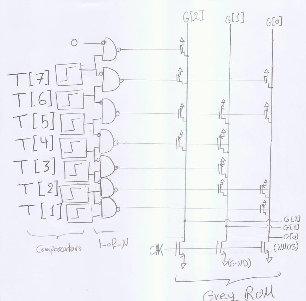
11 Problems (cont.) The encoder is composed of two parts, the one out of N (1-of-N) circuit and Gray ROM. The 1-of-N circuit is used to detect the 1 to 0 transition occurred in the Thermometer code which indicates the input voltage level, by an array of two input NAND logic gate with one input inverted ROM is actually a truth table in hardware form.next Figure shows an example of 3 bit Gray ROM based Thermometer to Gray encoder. Every input Thermometer code combination corresponds to an address, which is read to produce 3-bit Gray code. When the input in the non-inverted port is 1 and the inverted port 0 then only the output will be equal to 0. For the other input patterns the output will be equal to 1. In general if no bubble errors occurred there will only one 1 to 0 transition detected in the Thermometer code. So there will be only one 0 appearing at the output of 1-of-N circuit. This 0 signal used to enable the corresponding row in the Gray ROM. 11
12 Dec Thermometer code Grey Code Binary D T[7] T[6] T[5] T[4] T[3] T[2] T[1] G[2] G[1] G[0] B[2] B[1] B[0]
13 13
14 14
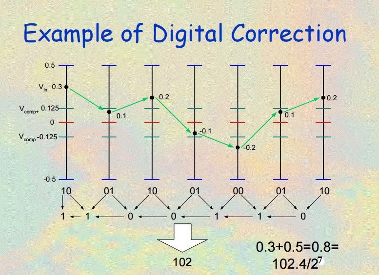
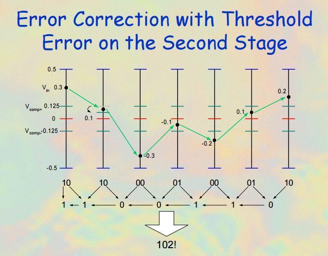
15 Problems (cont.) Now to understand how the Grey code encoding solves the problem of Metastability let s assume the case where the input voltage is almost equal the reference voltage of the 4th comparator hence T[4] is Metastable. thus we get a Thermometer code like this : 000X111 where X is undefined. Let s assume further that this X is interpreted as 1 and 0 by the 4th and 5th NAND gates respectively. Now both the 4th and 5th NAND gates will produce zero selecting the corresponding value stored in the ROM. In case of the Binary ROM: 4th NAND will enable B[2].But the 5th NAND will enable B[1] and B[2]. then the value obtained is 111 while either 011 or 100 was expected. In case of Gray ROM: 4th NAND will enable G[2] and G[1].But the 5th NAND will enable G[1]. And the value obtained will be 110 which is true. Gray-code encoding allows only one bit in the output to change at a time. The comparator outputs are first converted to gray-code encoding and then later decoded to binary. 15
16 Advantages and Disadvantages Advantages Very large Bandwidth A special nonlinear behaviour can be approached by varying the values of the resistors in the ladder, which could be used in some applications. Disadvantages Area (2 N -1 comparators) Power and Cost limited resolution (Max 8 or 10 bits) 16
17 Semi-Flash ADC For a trial to decrease the area and the number of comparators used. 2 flash ADCs are used, each will output half the number of bits; coarse ADC to output the most significant bits & fine ADC to output the least significant bits. The number of comparators are reduced drastically : Example: An 8-bit flash ADC has : (2^N - 1) ; N= 8 ; 255 comparators. An 8-bit semi-flash is realized by having two 4-bit flash ADCs (2^Nc -1) + ( 2^Nf -1) ; Nc = 4, Nf = 4 ; = = 30 comparators. 17
18 Semi-Flash ADC The Semi-Flash has 2 extra blocks : DAC & subtractor Thus the latency of this ADC would be more than 2 times of the Flash latency, because the coarse ADC waits for the output of the fine ADC. - An amplifier of G = 2^Nc would be added after subtractor -to avoid the small residue signals that are sensitive to noise. -to make the signal swing equal for both ADCs - to simplify the design, Both ADCs use same Ladder. 18

19 Pipelined ADC... Binary search.. 19

20 Pipelined ADC... Basic Architecture 20
 = 2 Vin - Vref if Vin > 1/2 Vref = 2 Vin if Vin < 1/2 Vref 21")
21 Pipelined ADC... To check in the binary tree: check polarity of Vin - α Vref. where α= ½, ¼ or ¾, ⅛ or ⅜ or ⅝ or ⅞,...so on α changes every stage!! But we need a recursive function.. Assume we have the function f=vres f(vin, Vref) = 2 Vin - Vref if Vin > 1/2 Vref = 2 Vin if Vin < 1/2 Vref 21
22 Pipelined ADC... For the 1st stage: if (Vin > ½ Vref ) then f(vin, Vref) = 2 Vin - Vref = 2*(Vin - ½ Vref) First check # else f(vin, Vref) = 2 Vin.Second check # end if; next stage it must be (Vin - ¾ Vref) for first check and (Vin - ¼ Vref) for second check.. 22
23 Pipelined ADC... For the 2nd stage: First check f(2 Vin - Vref, Vref) = 4 Vin - 2 Vref - Vref = 4*(Vin - ¾ Vref) Second Check f(2 Vin, Vref) = 4 Vin - Vref = 4*(Vin - ¼ Vref) *You can go on and check all the following steps to make sure you get the binary search right. 23

24 Pipelined ADC... MDAC Implementation.. 24

25 Pipelined ADC... Adding comparators to the design.. 25
. 2. Comparator offset: (ex, if -1mV input was read as 2 mv).")
26 Pipelined ADC... Fully differential from -Vref to Vref 1 Bit/stage ADC Over range problems due to: 1. gain/slope: (a result of capacitors mismatch). 2. Comparator offset: (ex, if -1mV input was read as 2 mv). 26
 = 2 Vin - Vref if Vin > ¼Vref = 2 Vin if")
27 Pipelined ADC bit/stage ADC: f(vin, Vref) = 2 Vin - Vref if Vin > ¼Vref = 2 Vin if -¼Vref < Vin < ¼Vref = 2 Vin + Vref if Vin < -¼Vref 27
28 Summary of an MDAC stage O/P Figure. MDAC structure

29 Summary of an MDAC stage Fig. Sampling and Conversion Configurations for an MDAC
30 Latency vs Throughput! Fig. Pipelined behavior of the ADC
31 - Stages operate on the input like a shift register. - New output data EVERY clock cycle, but each stage introduces at least one half clock Latency.
32 Digital Correction - The DCL is actually a simple circuit of Half & Full adders to add the LSB of the higher stage ( the error bit) to the MSB (certain bit) of the next stage.. The Last stage LSB is TRUNCATED! - As long as the individual thresholds deviate no more than V r /4 from an ideal value, then the error can be corrected by adding shifted digital outputs of each of the stages.
33
34
35 High Speed Problems - OpAmp Finite gain Sol? Use a high gain Cascode amplifier designed to give a 20dB gain around the sampling frequency. - Capacitances Mismatching & the appearance of parasitic capacitances Sol? Design the feedback gain of the OpAmp including Cp in the calculations Accurate capacitance matching between Cs and Cf.
36 High Speed Problems Fig. Cascode Structure Amplifier For High Gain
37 References SAR, Pipelined Versus. "A Tale of Two ADCs." IEEE SOLID-STATE CIRCUITS 39 (2015) Walt Kester, Analog-Digital Conversion, Analog Devices, 2004, ISBN
Analog-to-Digital i Converters
 CSE 577 Spring 2011 Analog-to-Digital i Converters Jaehyun Lim, Kyusun Choi Department t of Computer Science and Engineering i The Pennsylvania State University ADC Glossary DNL (differential nonlinearity)
Mixed-Signal-Electronics
 1 Mixed-Signal-Electronics PD Dr.-Ing. Stephan Henzler 2 Chapter 6 Nyquist Rate Analog-to-Digital Converters 3 Pipelined ADC 2 4 High-Speed ADC: Pipeline Processing Stephan Henzler Advanced Integrated
Tuesday, March 1st, 9:15 11:00. Snorre Aunet Nanoelectronics group Department of Informatics University of Oslo.
 Nyquist Analog to Digital it Converters Tuesday, March 1st, 9:15 11:00 Snorre Aunet (sa@ifi.uio.no) Nanoelectronics group Department of Informatics University of Oslo 3.1 Introduction 3.1.1 DAC applications
UNIVERSITY OF CALIFORNIA College of Engineering Department of Electrical Engineering and Computer Sciences
 UNIVERSITY OF CALIFORNIA College of Engineering Department of Electrical Engineering and Computer Sciences Final Exam EECS 247 H. Khorramabadi Tues., Dec. 14, 2010 FALL 2010 Name: SID: Total number of
The counterpart to a DAC is the ADC, which is generally a more complicated circuit. One of the most popular ADC circuit is the successive
 1 The counterpart to a DAC is the ADC, which is generally a more complicated circuit. One of the most popular ADC circuit is the successive approximation converter. 2 3 The idea of sampling is fully covered
IMPLEMENTING THE 10-BIT, 50MS/SEC PIPELINED ADC
 98 CHAPTER 5 IMPLEMENTING THE 0-BIT, 50MS/SEC PIPELINED ADC 99 5.0 INTRODUCTION This chapter is devoted to describe the implementation of a 0-bit, 50MS/sec pipelined ADC with different stage resolutions
Mixed-Signal-Electronics
 1 Mixed-Signal-Electronics PD Dr.-Ing. Stephan Henzler 2 Chapter 6 Nyquist Rate Analog-to-Digital Converters 3 Analog-to-Digital Converter Families Architecture Variant Speed Precision Counting Operation
EE247 Lecture 20. Comparator architecture examples Flash ADC sources of error Sparkle code Meta-stability
 EE247 Lecture 2 ADC Converters ADC architectures (continued) Comparator architectures Latched comparators Latched comparators incorporating preamplifier Sample-data comparators Offset cancellation Comparator
Design of Pipeline Analog to Digital Converter
 Design of Pipeline Analog to Digital Converter Vivek Tripathi, Chandrajit Debnath, Rakesh Malik STMicroelectronics The pipeline analog-to-digital converter (ADC) architecture is the most popular topology
A Novel ROM Architecture for Reducing Bubble and Metastability Errors in High Speed Flash ADCs
 1 A Novel ROM Architecture for Reducing Bubble and Metastability Errors in High Speed Flash ADCs Mustafijur Rahman, Member, IEEE, K. L. Baishnab, F. A. Talukdar, Member, IEEE Dept. of Electronics & Communication
The need for Data Converters
 The need for Data Converters ANALOG SIGNAL (Speech, Images, Sensors, Radar, etc.) PRE-PROCESSING (Filtering and analog to digital conversion) DIGITAL PROCESSOR (Microprocessor) POST-PROCESSING (Digital
CMOS High Speed A/D Converter Architectures
 CHAPTER 3 CMOS High Speed A/D Converter Architectures 3.1 Introduction In the previous chapter, basic key functions are examined with special emphasis on the power dissipation associated with its implementation.
EECS 247 Lecture 18: Data Converters- Track & Hold- ADC Design 2009 Page 1. EE247 Lecture 18
 EE247 Lecture 8 ADC Converters Sampling (continued) Bottom-plate switching Track & hold T/H circuits T/H combined with summing/difference function T/H circuit incorporating gain & offset cancellation T/H
Modeling and Implementation of A 6-Bit, 50MHz Pipelined ADC in CMOS
 Master s Thesis Modeling and Implementation of A 6-Bit, 50MHz Pipelined ADC in CMOS Qazi Omar Farooq Department of Electrical and Information Technology, Faculty of Engineering, LTH, Lund University, 2016.
RESIDUE AMPLIFIER PIPELINE ADC
 RESIDUE AMPLIFIER PIPELINE ADC A direct-conversion ADC designed only with Op-Amps Abstract This project explores the design of a type of direct-conversion ADC called a Residue Amplifier Pipeline ADC. Direct-conversion
Lecture #6: Analog-to-Digital Converter
 Lecture #6: Analog-to-Digital Converter All electrical signals in the real world are analog, and their waveforms are continuous in time. Since most signal processing is done digitally in discrete time,
Advantages of Analog Representation. Varies continuously, like the property being measured. Represents continuous values. See Figure 12.
 Analog Signals Signals that vary continuously throughout a defined range. Representative of many physical quantities, such as temperature and velocity. Usually a voltage or current level. Digital Signals
Lecture 9, ANIK. Data converters 1
 Lecture 9, ANIK Data converters 1 What did we do last time? Noise and distortion Understanding the simplest circuit noise Understanding some of the sources of distortion 502 of 530 What will we do today?
Design of an Assembly Line Structure ADC
 Design of an Assembly Line Structure ADC Chen Hu 1, Feng Xie 1,Ming Yin 1 1 Department of Electronic Engineering, Naval University of Engineering, Wuhan, China Abstract This paper presents a circuit design
Analog I/O. ECE 153B Sensor & Peripheral Interface Design Winter 2016
 Analog I/O ECE 153B Sensor & Peripheral Interface Design Introduction Anytime we need to monitor or control analog signals with a digital system, we require analogto-digital (ADC) and digital-to-analog
EE 421L Digital Electronics Laboratory. Laboratory Exercise #9 ADC and DAC
 EE 421L Digital Electronics Laboratory Laboratory Exercise #9 ADC and DAC Department of Electrical and Computer Engineering University of Nevada, at Las Vegas Objective: The purpose of this laboratory
Data Converters. Dr.Trushit Upadhyaya EC Department, CSPIT, CHARUSAT
 Data Converters Dr.Trushit Upadhyaya EC Department, CSPIT, CHARUSAT Purpose To convert digital values to analog voltages V OUT Digital Value Reference Voltage Digital Value DAC Analog Voltage Analog Quantity:
Deep-Submicron CMOS Design Methodology for High-Performance Low- Power Analog-to-Digital Converters
 Deep-Submicron CMOS Design Methodology for High-Performance Low- Power Analog-to-Digital Converters Abstract In this paper, we present a complete design methodology for high-performance low-power Analog-to-Digital
Design of Analog Integrated Systems (ECE 615) Outline
 Outline") Design of Analog Integrated Systems (ECE 615) Lecture 9 SAR and Cyclic (Algorithmic) Analog-to-Digital Converters Ayman H. Ismail Integrated Circuits Laboratory Ain Shams University Cairo, Egypt ayman.hassan@eng.asu.edu.eg
Design of Analog Integrated Systems (ECE 615) Lecture 9 SAR and Cyclic (Algorithmic) Analog-to-Digital Converters Ayman H. Ismail Integrated Circuits Laboratory Ain Shams University Cairo, Egypt ayman.hassan@eng.asu.edu.eg
2008 IEEE ASIA PACIFIC CONFERENCE ON CIRCUITS AND SYSTEMS
 2008 IEEE ASIA PACIFIC CONFERENCE ON CIRCUITS AND SYSTEMS November 30 - December 3, 2008 Venetian Macao Resort-Hotel Macao, China IEEE Catalog Number: CFP08APC-USB ISBN: 978-1-4244-2342-2 Library of Congress:
Summary of Last Lecture
 EE247 Lecture 2 ADC Converters (continued) Successive approximation ADCs (continued) Flash ADC Flash ADC sources of error Sparkle code Meta-stability Comparator design EECS 247 Lecture 2: Data Converters
4 Bits 250MHz Sampling Rate CMOS Pipelined Analog-to-Digital Converter
 4 Bits 250MHz Sampling Rate CMOS Pipelined Analog-to-Digital Converter Jinrong Wang B.Sc. Ningbo University Supervisor: dr.ir. Wouter A. Serdijn Submitted to The Faculty of Electrical Engineering, Mathematics
Assoc. Prof. Dr. Burak Kelleci
 DEPARTMENT OF ELECTRICAL &ELECTRONICS ENGINEERING ANALOG-TO-DIGITAL AND DIGITAL- TO-ANALOG CONVERTERS Assoc. Prof. Dr. Burak Kelleci Fall 2018 OUTLINE Nyquist-Rate DAC Thermometer-Code Converter Hybrid
Another way to implement a folding ADC
 Another way to implement a folding ADC J. Van Valburg and R. van de Plassche, An 8-b 650 MHz Folding ADC, IEEE JSSC, vol 27, #12, pp. 1662-6, Dec 1992 Coupled Differential Pair J. Van Valburg and R. van
CHAPTER 3 DESIGN OF PIPELINED ADC USING SCS-CDS AND OP-AMP SHARING TECHNIQUE
 CHAPTER 3 DESIGN OF PIPELINED ADC USING SCS-CDS AND OP-AMP SHARING TECHNIQUE 3.1 INTRODUCTION An ADC is a device which converts a continuous quantity into discrete digital signal. Among its types, pipelined
2. ADC Architectures and CMOS Circuits
 /58 2. Architectures and CMOS Circuits Francesc Serra Graells francesc.serra.graells@uab.cat Departament de Microelectrònica i Sistemes Electrònics Universitat Autònoma de Barcelona paco.serra@imb-cnm.csic.es
A-D and D-A Converters
 Chapter 5 A-D and D-A Converters (No mathematical derivations) 04 Hours 08 Marks When digital devices are to be interfaced with analog devices (or vice a versa), Digital to Analog converter and Analog
A Digitally Enhanced 1.8-V 15-b 40- Msample/s CMOS Pipelined ADC
 A Digitally Enhanced.8-V 5-b 4- Msample/s CMOS d ADC Eric Siragusa and Ian Galton University of California San Diego Now with Analog Devices San Diego California Outline Conventional PADC Example Digitally
CMOS ADC & DAC Principles
 CMOS ADC & DAC Principles Willy Sansen KULeuven, ESAT-MICAS Leuven, Belgium willy.sansen@esat.kuleuven.be Willy Sansen 10-05 201 Table of contents Definitions Digital-to-analog converters Resistive Capacitive
Administrative. No office hour on Thurs. this week Instead, office hour 3 to 4pm on Wed.
 Administrative No office hour on Thurs. this week Instead, office hour 3 to 4pm on Wed. EECS 247 Lecture 2 Nyquist Rate ADC: Architecture & Design 27 H.K. Page EE247 Lecture 2 ADC Converters Sampling (continued)
Outline. Analog/Digital Conversion
 Analog/Digital Conversion The real world is analog. Interfacing a microprocessor-based system to real-world devices often requires conversion between the microprocessor s digital representation of values
10. Chapter: A/D and D/A converter principles
 Punčochář, Mohylová: TELO, Chapter 10: A/D and D/A converter principles 1 10. Chapter: A/D and D/A converter principles Time of study: 6 hours Goals: the student should be able to define basic principles
Proposing. An Interpolated Pipeline ADC
 Proposing An Interpolated Pipeline ADC Akira Matsuzawa Tokyo Institute of Technology, Japan Matsuzawa & Okada Lab. Background 38GHz long range mm-wave system Role of long range mm-wave Current Optical
CONTINUOUS DIGITAL CALIBRATION OF PIPELINED A/D CONVERTERS
 CONTINUOUS DIGITAL CALIBRATION OF PIPELINED A/D CONVERTERS By Alma Delić-Ibukić B.S. University of Maine, 2002 A THESIS Submitted in Partial Fulfillment of the Requirements for the Degree of Master of
AD Bit, 20/40/65 MSPS 3 V Low Power A/D Converter. Preliminary Technical Data
 FEATURES Ultra Low Power 90mW @ 0MSPS; 135mW @ 40MSPS; 190mW @ 65MSPS SNR = 66.5 dbc (to Nyquist); SFDR = 8 dbc @.4MHz Analog Input ENOB = 10.5 bits DNL=± 0.5 LSB Differential Input with 500MHz Full Power
Fig. 2. Schematic of the THA. M1 M2 M3 M4 Vbias Vdd. Fig. 1. Simple 3-Bit Flash ADC. Table1. THA Design Values ( with 0.
 A 2-GSPS 4-Bit Flash A/D Converter Using Multiple Track/Hold Amplifiers By Dr. Mahmoud Fawzy Wagdy, Professor And Chun-Shou (Charlie) Huang, MSEE Department of Electrical Engineering, California State
Analysis of the system level design of a 1.5 bit/stage pipeline ADC 1 Amit Kumar Tripathi, 2 Rishi Singhal, 3 Anurag Verma
 014 Fourth International Conference on Advanced Computing & Communication Technologies Analysis of the system level design of a 1.5 bit/stage pipeline ADC 1 Amit Kumar Tripathi, Rishi Singhal, 3 Anurag
Low-Power Pipelined ADC Design for Wireless LANs
 Low-Power Pipelined ADC Design for Wireless LANs J. Arias, D. Bisbal, J. San Pablo, L. Quintanilla, L. Enriquez, J. Vicente, J. Barbolla Dept. de Electricidad y Electrónica, E.T.S.I. de Telecomunicación,
Analogue to Digital Conversion
 Analogue to Digital Conversion Turns electrical input (voltage/current) into numeric value Parameters and requirements Resolution the granularity of the digital values Integral NonLinearity proportionality
Chapter 2 Signal Conditioning, Propagation, and Conversion
 09/0 PHY 4330 Instrumentation I Chapter Signal Conditioning, Propagation, and Conversion. Amplification (Review of Op-amps) Reference: D. A. Bell, Operational Amplifiers Applications, Troubleshooting,
CHAPTER ELEVEN - Interfacing With the Analog World
 CHAPTER ELEVEN - Interfacing With the Analog World 11.1 (a) Analog output = (K) x (digital input) (b) Smallest change that can occur in the analog output as a result of a change in the digital input. (c)
High Speed Flash Analog to Digital Converters
 ECE 551, Analog Integrated Circuit Design, High Speed Flash ADCs, Dec 2005 1 High Speed Flash Analog to Digital Converters Alireza Mahmoodi Abstract Flash analog-to-digital converters, also known as parallel
A 14b 40Msample/s Pipelined ADC with DFCA
 A 14b 40Msample/s Pipelined ADC with DFCA Paul Yu, Shereef Shehata, Ashutosh Joharapurkar, Pankaj Chugh, Alex Bugeja, Xiaohong Du, Sung-Ung Kwak, Yiannis Papantonopoulos, Turker Kuyel Texas Instruments,
Optimizing the Stage Resolution of a 10-Bit, 50 Ms/Sec Pipelined A/D Converter & Its Impact on Speed, Power, Area, and Linearity
 Circuits and Systems, 202, 3, 66-75 http://dx.doi.org/0.4236/cs.202.32022 Published Online April 202 (http://www.scirp.org/journal/cs) Optimizing the Stage Resolution of a 0-Bit, 50 Ms/Sec Pipelined A/D
A 42 fj 8-bit 1.0-GS/s folding and interpolating ADC with 1 GHz signal bandwidth
 LETTER IEICE Electronics Express, Vol.11, No.2, 1 9 A 42 fj 8-bit 1.0-GS/s folding and interpolating ADC with 1 GHz signal bandwidth Mingshuo Wang a), Fan Ye, Wei Li, and Junyan Ren b) State Key Laboratory
12-Bit Pipeline ADC Implemented in 0.09-um Digital CMOS Technology for Powerline Alliance
 2-Bit Pipeline ADC Implemented in 0.09-um Digital CMOS Technology for Powerline Alliance Olga Joy L. Gerasta, Lavern S. Bete, Jayson C. Loreto, Sheerah Dale M. Orlasan, and Honey Mae N. Tagalogon Microelectronics
Analog to Digital Converters
 Analog to Digital Converters By: Byron Johns, Danny Carpenter Stephanie Pohl, Harry Bo Marr http://ume.gatech.edu/mechatronics_course/fadc_f05.ppt (unless otherwise marked) Presentation Outline Introduction:
Quad 12-Bit Digital-to-Analog Converter (Serial Interface)
") Quad 1-Bit Digital-to-Analog Converter (Serial Interface) FEATURES COMPLETE QUAD DAC INCLUDES INTERNAL REFERENCES AND OUTPUT AMPLIFIERS GUARANTEED SPECIFICATIONS OVER TEMPERATURE GUARANTEED MONOTONIC OVER
Quad 1-Bit Digital-to-Analog Converter (Serial Interface) FEATURES COMPLETE QUAD DAC INCLUDES INTERNAL REFERENCES AND OUTPUT AMPLIFIERS GUARANTEED SPECIFICATIONS OVER TEMPERATURE GUARANTEED MONOTONIC OVER
ELG3336: Converters Analog to Digital Converters (ADCs) Digital to Analog Converters (DACs)
 Digital to Analog Converters (DACs)") ELG3336: Converters Analog to Digital Converters (ADCs) Digital to Analog Converters (DACs) Digital Output Dout 111 110 101 100 011 010 001 000 ΔV, V LSB V ref 8 V FSR 4 V 8 ref 7 V 8 ref Analog Input
ELG3336: Converters Analog to Digital Converters (ADCs) Digital to Analog Converters (DACs) Digital Output Dout 111 110 101 100 011 010 001 000 ΔV, V LSB V ref 8 V FSR 4 V 8 ref 7 V 8 ref Analog Input
The Importance of Data Converter Static Specifications Don't Lose Sight of the Basics! by Walt Kester
 TUTORIAL The Importance of Data Converter Static Specifications Don't Lose Sight of the Basics! INTRODUCTION by Walt Kester In the 1950s and 1960s, dc performance specifications such as integral nonlinearity,
LAYOUT IMPLEMENTATION OF A 10-BIT 1.2 GS/s DIGITAL-TO-ANALOG CONVERTER IN 90nm CMOS
 LAYOUT IMPLEMENTATION OF A 10-BIT 1.2 GS/s DIGITAL-TO-ANALOG CONVERTER IN 90nm CMOS A thesis submitted in partial fulfilment of the requirements for the degree of Master of Science in Electrical Engineering
Design of an 8-bit Successive Approximation Pipelined Analog to Digital Converter (SAP- ADC) in 90 nm CMOS
 in 90 nm CMOS") Design of an 8-bit Successive Approximation Pipelined Analog to Digital Converter (SAP- ADC) in 90 nm CMOS A thesis submitted in partial fulfillment of the requirements for the degree of Master of Science
Design of an 8-bit Successive Approximation Pipelined Analog to Digital Converter (SAP- ADC) in 90 nm CMOS A thesis submitted in partial fulfillment of the requirements for the degree of Master of Science
Chapter 2 ADC Architecture
 Chapter 2 ADC Architecture 2.1 Introduction While lots of Nyquist-rate ADCs are proposed to resolve resolutions at different speeds throughout the years, there are three types of architectures most widely
INTEGRATED CIRCUITS. AN109 Microprocessor-compatible DACs Dec
 INTEGRATED CIRCUITS 1988 Dec DAC products are designed to convert a digital code to an analog signal. Since a common source of digital signals is the data bus of a microprocessor, DAC circuits that are
Design of 1.8V, 72MS/s 12 Bit Pipeline ADC in 0.18µm Technology
 Design of 1.8V, 72MS/s 12 Bit Pipeline ADC in 0.18µm Technology Ravi Kumar 1, Seema Kanathe 2 ¹PG Scholar, Department of Electronics and Communication, Suresh GyanVihar University, Jaipur, India ²Assistant
Chapter 3 Novel Digital-to-Analog Converter with Gamma Correction for On-Panel Data Driver
 Chapter 3 Novel Digital-to-Analog Converter with Gamma Correction for On-Panel Data Driver 3.1 INTRODUCTION As last chapter description, we know that there is a nonlinearity relationship between luminance
A Successive Approximation ADC based on a new Segmented DAC
 A Successive Approximation ADC based on a new Segmented DAC segmented current-mode DAC successive approximation ADC bi-direction segmented current-mode DAC DAC INL 0.47 LSB DNL 0.154 LSB DAC 3V 8 2MS/s
UNIT III Data Acquisition & Microcontroller System. Mr. Manoj Rajale
 UNIT III Data Acquisition & Microcontroller System Mr. Manoj Rajale Syllabus Interfacing of Sensors / Actuators to DAQ system, Bit width, Sampling theorem, Sampling Frequency, Aliasing, Sample and hold
EE247 Lecture 23. EECS 247 Lecture 23 Pipelined ADCs 2008 H.K. Page 1. Pipeline ADC Block Diagram DAC ADC. V res2. Stage 2 B 2.
 EE247 Lecture 23 Pipelined ADCs (continued) Effect gain stage, sub-dac non-idealities on overall ADC performance Digital calibration (continued) Correction for inter-stage gain nonlinearity Implementation
Fundamentals of Data Converters. DAVID KRESS Director of Technical Marketing
 Fundamentals of Data Converters DAVID KRESS Director of Technical Marketing 9/14/2016 Analog to Electronic Signal Processing Sensor (INPUT) Amp Converter Digital Processor Actuator (OUTPUT) Amp Converter
NPTEL. VLSI Data Conversion Circuits - Video course. Electronics & Communication Engineering.
 NPTEL Syllabus VLSI Data Conversion Circuits - Video course COURSE OUTLINE This course covers the analysis and design of CMOS Analog-to-Digital and Digital-to-Analog Converters,with about 7 design assigments.
UCLA UCLA Electronic Theses and Dissertations
 UCLA UCLA Electronic Theses and Dissertations Title An 11-bit 20MS/s Pipelined Analog-to-Digital Converter with Op Amp Sharing Permalink https://escholarship.org/uc/item/0bg2v018 Author Kong, Long Publication
Implementing a 5-bit Folding and Interpolating Analog to Digital Converter
 Implementing a 5-bit Folding and Interpolating Analog to Digital Converter Zachary A Pfeffer (pfefferz@colorado.edu) Department of Electrical and Computer Engineering University of Colorado, Boulder CO
A NEW APPROACH TO DESIGN LOW POWER CMOS FLASH A/D CONVERTER
 A NEW APPROACH TO DESIGN LOW POWER CMOS FLASH A/D CONVERTER C Mohan¹ and T Ravisekhar 2 ¹M. Tech (VLSI) Student, Sree Vidyanikethan Engineering College (Autonomous), Tirupati, India 2 Assistant Professor,
Summary Last Lecture
 Interleaved ADCs EE47 Lecture 4 Oversampled ADCs Why oversampling? Pulse-count modulation Sigma-delta modulation 1-Bit quantization Quantization error (noise) spectrum SQNR analysis Limit cycle oscillations
Summary Last Lecture
 EE247 Lecture 23 Converters Techniques to reduce flash complexity Interpolating (continued) Folding Multi-Step s Two-Step flash Pipelined s EECS 247 Lecture 23: Data Converters 26 H.K. Page Summary Last
A 10-bit, 100 MS/s Analog-to-Digital Converter in 1-µm CMOS
 A 10-bit, 100 MS/s Analog-to-Digital Converter in 1-µm CMOS FINAL REPOR EPORT Kwang Young Kim Integrated Circuits & Systems Laboratory Electrical Engineering Department University of California Los Angeles,
Data Converters. Lecture Fall2013 Page 1
 Data Converters Lecture Fall2013 Page 1 Lecture Fall2013 Page 2 Representing Real Numbers Limited # of Bits Many physically-based values are best represented with realnumbers as opposed to a discrete number
ANALOG TO DIGITAL (ADC) and DIGITAL TO ANALOG CONVERTERS (DAC)
 and DIGITAL TO ANALOG CONVERTERS (DAC)") COURSE / CODE DIGITAL SYSTEM FUNDAMENTALS (ECE421) DIGITAL ELECTRONICS FUNDAMENTAL (ECE422) ANALOG TO DIGITAL (ADC) and DIGITAL TO ANALOG CONVERTERS (DAC) Connecting digital circuitry to sensor devices
COURSE / CODE DIGITAL SYSTEM FUNDAMENTALS (ECE421) DIGITAL ELECTRONICS FUNDAMENTAL (ECE422) ANALOG TO DIGITAL (ADC) and DIGITAL TO ANALOG CONVERTERS (DAC) Connecting digital circuitry to sensor devices
Digital Calibration for Current-Steering DAC Linearity Enhancement
 Digital Calibration for Current-Steering DAC Linearity Enhancement Faculty of Science and Technology, Division of Electronics & Informatics Gunma University Shaiful Nizam Mohyar, Haruo Kobayashi Gunma
8-Bit, high-speed, µp-compatible A/D converter with track/hold function ADC0820
 8-Bit, high-speed, µp-compatible A/D converter with DESCRIPTION By using a half-flash conversion technique, the 8-bit CMOS A/D offers a 1.5µs conversion time while dissipating a maximum 75mW of power.
Analog to Digital Conversion
 Analog to Digital Conversion Florian Erdinger Lehrstuhl für Schaltungstechnik und Simulation Technische Informatik der Uni Heidelberg VLSI Design - Mixed Mode Simulation F. Erdinger, ZITI, Uni Heidelberg
Analogue to Digital Conversion
 Analogue to Digital Conversion Turns electrical input (voltage/current) into numeric value Parameters and requirements Resolution the granularity of the digital values Integral NonLinearity proportionality
EE 435. Lecture 41. ADC Design
 EE 435 Lecture 4 ADC Design Nyqyist ate Usage Structures. eview from last lecture. 0 esolution 6 SA Pipeline 8 4 Flash K 0K 00K M 0M 00M G 0G Speed . eview from last lecture. SA ADC C LK IN EF DAC n DAC
Index terms: Analog to digital converter, Flash ADC, Pseudo NMOS logic, Pseudo Dynamic CMOS logic multi threshold voltage CMOS inverters.
 Low Power CMOS Flash ADC C Mohan, T Ravisekhar Abstract The present investigation proposes an efficient low power encoding scheme intended for a flash analog to digital converter. The designing of a thermometer
Find Those Elusive ADC Sparkle Codes and Metastable States. by Walt Kester
 TUTORIAL Find Those Elusive ADC Sparkle Codes and Metastable States INTRODUCTION by Walt Kester A major concern in the design of digital communications systems is the bit error rate (BER). The effect of
Optimizing the Number of Bits/Stage in 10-Bit, 50Ms/Sec Pipelined A/D Converter Considering Area, Speed, Power and Linearity
 Optimizing the Number of Bits/Stage in 10-Bit, 50Ms/Sec Pipelined /D Converter Considering rea, Speed, Power and Linearity P. Prasad Rao, K. Lal Kishore bstract Pipeline DCs are becoming popular at high
L10: Analog Building Blocks (OpAmps,, A/D, D/A)
") L10: Analog Building Blocks (OpAmps,, A/D, D/A) Acknowledgement: Materials in this lecture are courtesy of the following sources and are used with permission. Dave Wentzloff 1 Introduction to Operational
L10: Analog Building Blocks (OpAmps,, A/D, D/A) Acknowledgement: Materials in this lecture are courtesy of the following sources and are used with permission. Dave Wentzloff 1 Introduction to Operational
DESIGN OF FOLDING CIRCUIT AND SAMPLE AND HOLD FOR 6 BIT ADC
 DESIGN OF FOLDING CIRCUIT AND SAMPLE AND HOLD FOR 6 BIT ADC Prajeesh R 1, Manukrishna V R 2, Bellamkonda Saidilu 3 1 Assistant Professor, ECE Department, SVNCE, Mavelikara, Kerala, (India) 2,3 PhD Research
ECE 6770 FINAL PROJECT
 ECE 6770 FINAL PROJECT POINT TO POINT COMMUNICATION SYSTEM Submitted By: Omkar Iyer (Omkar_iyer82@yahoo.com) Vamsi K. Mudarapu (m_vamsi_krishna@yahoo.com) MOTIVATION Often in the real world we have situations
L9: Analog Building Blocks (OpAmps,, A/D, D/A)
") L9: Analog Building Blocks (OpAmps,, A/D, D/A) Acknowledgement: Dave Wentzloff Introduction to Operational Amplifiers DC Model Typically very high input resistance ~ 300KΩ v id in a v id out High DC gain
L9: Analog Building Blocks (OpAmps,, A/D, D/A) Acknowledgement: Dave Wentzloff Introduction to Operational Amplifiers DC Model Typically very high input resistance ~ 300KΩ v id in a v id out High DC gain
P a g e 1. Introduction
 P a g e 1 Introduction 1. Signals in digital form are more convenient than analog form for processing and control operation. 2. Real world signals originated from temperature, pressure, flow rate, force
High Speed System Applications
 High Speed System Applications 1. High Speed Data Conversion Overview 2. Optimizing Data Converter Interfaces 3. DACs, DDSs, PLLs, and Clock Distribution 4. PC Board Layout and Design Tools Copyright 2006
Lecture 3 Switched-Capacitor Circuits Trevor Caldwell
 Advanced Analog Circuits Lecture 3 Switched-Capacitor Circuits Trevor Caldwell trevor.caldwell@analog.com Lecture Plan Date Lecture (Wednesday 2-4pm) Reference Homework 2017-01-11 1 MOD1 & MOD2 ST 2, 3,
L9: Analog Building Blocks (OpAmps, A/D, D/A)
") L9: Analog Building Blocks (OpAmps, A/D, D/A) Courtesy of Dave Wentzloff. Used with permission. 1 Introduction to Operational Amplifiers v id in DC Model a v id LM741 Pinout out 10 to 15V Typically very
L9: Analog Building Blocks (OpAmps, A/D, D/A) Courtesy of Dave Wentzloff. Used with permission. 1 Introduction to Operational Amplifiers v id in DC Model a v id LM741 Pinout out 10 to 15V Typically very
Electronics A/D and D/A converters
 Electronics A/D and D/A converters Prof. Márta Rencz, Gábor Takács, Dr. György Bognár, Dr. Péter G. Szabó BME DED December 1, 2014 1 / 26 Introduction The world is analog, signal processing nowadays is
How do ADCs work? Martin Rowe, Senior Technical Editor -- 7/1/2002 Test & Measurement World

A 7 bit 3.52 GHz Current Steering DAC for WiGig Applications
 A 7 bit 3.52 GHz Current Steering DAC for WiGig Applications Trindade, M. Helena Abstract This paper presents a Digital to Analog Converter (DAC) with 7 bit resolution and a sampling rate of 3.52 GHz to
Behavioral Simulator of Analog-to-Digital Converters
 Behavioral Simulator of Analog-to-Digital Converters Grzegorz Zareba Olgierd. A. Palusinski University of Arizona Outline Introduction and Motivation Behavioral Simulator of Analog-to-Digital Converters
Summary Last Lecture
 EE247 Lecture 23 Converters Techniques to reduce flash complexity Interpolating (continued) Folding Multi-Step s Two-Step flash Pipelined s EECS 247 Lecture 23: Data Converters 26 H.K. Page 1 Summary Last
A 2-bit/step SAR ADC structure with one radix-4 DAC
 A 2-bit/step SAR ADC structure with one radix-4 DAC M. H. M. Larijani and M. B. Ghaznavi-Ghoushchi a) School of Engineering, Shahed University, Tehran, Iran a) ghaznavi@shahed.ac.ir Abstract: In this letter,
Final Exam Spring 2012
 1 EE 435 Final Exam Spring 2012 Name Instructions: This is an open-book, open-notes, open computer exam but no collaboration either personal or electronic with anyone except the course instructor is permitted.
A REVIEW ON 4 BIT FLASH ANALOG TO DIGITAL CONVERTOR
 RESEARCH ARTICLE OPEN ACCESS A REVIEW ON 4 BIT FLASH ANALOG TO DIGITAL CONVERTOR Vijay V. Chakole 1, Prof. S. R. Vaidya 2, Prof. M. N. Thakre 3 1 MTech Scholar, S. D. College of Engineering, Selukate,
Lec. 8: Subranging/Two-step ADCs
 In The Name of Almighty Lec. 8: Subranging/Two-step ADCs Lecturer: Hooman Farkhani Department of Electrical Engineering Islamic Azad University of Najafabad Feb. 2016. Email: H_farkhani@yahoo.com General