20 GHz Low Power QVCO and De-skew Techniques in 0.13µm Digital CMOS. Masum Hossain & Tony Chan Carusone University of Toronto
|
|
|
- Judith Williams
- 6 years ago
- Views:
Transcription
1 20 GHz Low Power QVCO and De-skew Techniques in 0.13µm Digital CMOS Masum Hossain & Tony Chan Carusone University of Toronto
2 Motivation Data Rx3 Rx2 D-FF D-FF Rx1 D-FF Clock Clock Deskew Clock Deskew Deskew Shared Clock Source f ref PD LPF 1
3 Motivation Data Rx3 Rx2 D-FF D-FF Rx1 D-FF Clock Clock Deskew Clock Deskew Deskew Jitter Filter DCC (optional) Shared Clock Source Deskew 2
4 Outline Low power clock source in Digital CMOS Review of CMOS LC VCO topology Colpitts vs Cross-coupled Proposed VCO topology Experimental Results Low power clock deskew technique CMOS Review of existing deskew techniques Proposed deskew technique Experimental Results 3
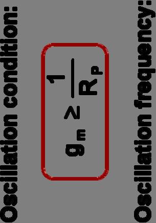
5 Cross-Coupled VCO L R P C L -1 C var M 1 (g m ) 4
6 Colpitts VCO Conventional Colpitts Modified Colpitts L R P C L [Nguyen 92] R L C L L M 1 (g m ) M 1 (g m ) C 1 R P C 1 C var C var Decouples the tank from load 5
 C")

7 Colpitts VCO R L C L L L R P Z in C 1 M 1 (g m ) C var R P R = C eq g m 2 ω C1Cvar C1C = C + C 1 var var 6
8 Proposed VCO Cross-Coupled L R P C L Colpitts R L C L L R L C L L -1 M 2 (g m2 ) M 1 (g m ) M 1 C var (g m ) R C GS -1 C var R P C 1 C var M 1 (g m1 ) Less g m required f osc depends on C L More g m required f osc independent of C L 7
9 Proposed VCO L R L C L Y x L v C g m2 v GS 1 R L C L M 2 (g m2 ) i x R C GS C var C var v x -1 M 1 (g m1 ) R P (-1/g m1 ) 8
10 VCO Summary Frequency of Oscillation Minimum Required g m Cross- Coupled f osc ( ( )) 2π L C + C 1 = var L 1 R P Colpitts f osc = 2π L C 1C C + C 1 var var 1 4 R P Proposed VCO f osc = 2π L C C GS GS C + C var var 1 1 C var g m 2 R P C GS Proposed oscillator combines the benefit of both topology! 9
11 QVCO Implementation To scope Off-chip 50-ohm term. V DD = 1.2 V On die 300 um T. Line 50-ohm V bias 50-ohm M 2 C- C+ C- C+ In+ C- C+ In- I-VCO In+ In- Q-VCO In+ In- M 1 M C 10

12 QVCO Implementation 650 um 90 o 400 um 270 o 0 o 180 o Metal Dummy Fill 11
 Pout (dbm) Tuning range 2.")
13 QVCO Performance Frequency (GHz) V control (V) Pout (dbm) Tuning range 2.4 GHz (~12%) 12

14 QVCO Performance Frequency (GHz) V control (V) Pout (dbm) 13
 Pout (dbm) Cable loss was de-embedded 14")
15 QVCO Performance Frequency (GHz) V control (V) Pout (dbm) Cable loss was de-embedded 14

 Phase Noise = -48.")
16 Phase Noise(dBc/Hz) 1 MHz offset) QVCO Performance Frequency (GHz) Pout (dbm) Phase Noise = log 10 (RBW) = dbc/hz 15
17 Phase Noise(dBc/Hz) 1 MHz offset) QVCO Performance P DC =20 mw P DC =30 mw Frequency (GHz) Phase Noise = log 10 (RBW) = dbc/hz 16
18 Performance Comparison CSICS 06 CSICS 06 JSSC 07 JSSC 04 VLSI 05 This work Technology 90-nm CMOS 90-nm CMOS 0.13-um CMOS 0.13-um CMOS 90-nm SOI 0.13-um CMOS Frequency 10 GHz 10 GHz 26 GHz 10 GHz 40 GHz 20 GHz Topology Colpitts Cross- Coupled G m Tuned Cross- Coupled Cross- Coupled Cross- Coupled Diff./Quadrature Diff. Diff. Diff. Quad. Quad. Quad. Tuning Range 12.2 % 15.8 % 23.6 % 15% 12.5 % 12 % Inductor Q Phase Noise (dbc/hz@1 MHz) MHz VCO power VCO+ Buffer 36 mw 7.5 mw 17.5 mw 43.6 mw 50 mw 14.4 mw mw mW FOM (VCO) (db) (VCO+ Buffer)
19 Deskew Techniques Mux/Interpolator 2f 0 T-FF f inj θ inj V control θ out -θ inj θ out 90 o 0 o 90 o [Maneatis 96] deskew Moderate power Supply Noise Duty Cycle Dis. All pass JTF 0 o [ Takauchi 03 Kromer 06] deskew Simple architecture Uses 2f 0 or 4 phase Non-linearity All pass JTF f osc -f inj [Zhang 06 O mahony 08] Less supply noise Less DCD Low pass JTF Low power Limited deskew (<360) Non-linearity Skew dependent JTF 18
20 Passive Injection Technique V INJ V INJ L R L R


 θ out R")

21 ILO based deskew I INJ θ inj L M 2 V OUT (g m2 ) θ out R -1 I OSC θ osc M 1 (g m1 ) 20
![ILO based deskew (K=0.1) 100 Deskew (deg.) Deskewed clock 50 225 mv 0-50 Simulated [k=0.1] Measured [k=0.1] -100 18.6 18.](/docs-images/74/69928615/images/22-0.jpg "8 19 19.2 19.4 f osc (GHz) 4.")
22 ILO based deskew (K=0.1) 100 Deskew (deg.) Deskewed clock mv 0-50 Simulated [k=0.1] Measured [k=0.1] f osc (GHz) 4.5 X Clock amplification Less than 10% amplitude variation 12 mw power consumption Deskew << 180 o 50 mv 21
23 ILO based deskew (K=0.2) Deskew (deg.) K=0.2 K=0.1 Sim. Sim. Meas. Meas f osc (GHz) 2.25 X Clock amplification More than 30% amplitude variation 12 mw power consumption Deskew range increases but non-linear 100 mv 22
24 Jitter Transfer Function Input clock Spectrum Analyzer Output clock VCO Jitter TF Input Jitter TF V control f highpass Freq. f lowpass Freq RBW = 100 khz 10 db 5 MHz K=0.02 K=0.1 Output clock Input clock 19 GHz 23

25 Jitter Transfer Function Input clock Spectrum Analyzer Output clock VCO Jitter TF Higher K Input Jitter TF Higher K V control Freq. Freq RBW = 100 khz 10 db 5 MHz K=0.02 K=0.2 Output clock Input clock 19 GHz 24

26 Jitter of Deskewed Clock Sim. Meas dbc/hz (Ref. VCO) -107 dbc/hz (20 o ) -110 dbc/hz (0 o ) 25
 -99 dbc/hz (90 o ) -110 dbc/hz (0 o ) 26")
27 Jitter of Deskewed Clock Sim. Meas dbc/hz (Ref. VCO) -99 dbc/hz (90 o ) -110 dbc/hz (0 o ) 26
28 Summary: ILO Based Deskew Deskew (deg.) Nonlinear Region Linear Region Sim. Meas f osc (GHz) Nonlinear Region Linear Region (deskew< 50 o ) Amplitude variation <10% Linear phase steps 12 db jitter 0 o 9 +/- 25 o Nonlinear Region (deskew> 50 o ) Amplitude variation >20% Non-linear phase steps No jitter reduction at 90 o Motivation: Achieve o deskew range using only the linear region 27
29 Proposed Deskew Technique θ out I-VCO V control Q-VCO θ out VCO V control θ inj Binary Selection [1/0] θ inj θ out -θ inj A θ out -θ inj f osc -f inj f osc -f inj B 28
30 Proposed Deskew Technique θ out I-VCO V control Q-VCO θ out VCO V control θ inj Binary Selection [1/0] θ inj θ out -θ inj A θ out -θ inj C 90 o B f osc -f inj f osc -f inj D 29
31 Proposed Deskew Technique θ out I-VCO V control Q-VCO K=.125 Clock Amp=11.48 db θ inj Binary Selection [1/0] Deskew (deg.) Sim. Meas f osc (GHz) 30
32 Proposed Deskew Technique θ out I-VCO V control Q-VCO K=.125 Clock Amp=11.48 db Less Amplitude variation 200 θ inj Binary Selection [1/0] Deskew (deg.) I-VCO Q-VCO f osc (GHz) 31
33 Proposed Deskew Technique θ out V control I-VCO Q-VCO 200 θ inj Binary Selection [1/0] Deskew (deg.) B I-VCO Q-VCO A f osc (GHz) 32
34 Proposed Deskew Technique θ out V control I-VCO Q-VCO DCB A 200 θ inj Binary Selection [1/0] Deskew (deg.) B D I-VCO Q-VCO A C f osc (GHz) 33
35 Proposed Deskew Technique Deskew (deg.) 200 I-VCO 100 E B 0 F D -100 Q-VCO A C -98 dbc/hz (Ref. VCO) F (-109 dbc/hz) E(-108 dbc/hz) f osc (GHz) 34
 200 I-VCO 100 E B 0 F D -100 Q-VCO A C")
 D (-104 dbc/hz) B (-105 dbc/hz) -200")
36 Proposed Deskew Technique Deskew (deg.) 200 I-VCO 100 E B 0 F D -100 Q-VCO A C -98 dbc/hz (Ref. VCO) D (-104 dbc/hz) B (-105 dbc/hz) f osc (GHz) 35
37 Comparison and Summary Phase Noise(dBc/Hz) 1 MHz offset) Using Q VCO Using Diff VCO Deskew (deg.) We have introduced: Low power Q-VCO topology for high-speed applications Utilize the QVCO based Deskew technique with inherent clock amplification and jitter filtering 36
38 Acknowledgements Intel Circuit Research Lab: F. O Mahony, M. Mansuri & B. Casper for their contribution in clock deskew technique presented in this work Gennum Corporation: For providing design & fabrication facilities 37

39 Backup Slide: Calibration Trigger Source Channel 3 Channel 3 Delay Channel 4 Delay Channel 4 30 mv 10 ps 39

40 Backup Slide: Additional Verification The same technique is also applicable with quadrature ring oscillator 40
CMOS Oscillators for Clock Distribution and Injection-Locked Deskew Masum Hossain and Anthony Chan Carusone, Senior Member, IEEE
 2138 IEEE JOURNAL OF SOLID-STATE CIRCUITS, VOL. 44, NO. 8, AUGUST 2009 CMOS Oscillators for Clock Distribution and Injection-Locked Deskew Masum Hossain and Anthony Chan Carusone, Senior Member, IEEE Abstract
95GHz Receiver with Fundamental Frequency VCO and Static Frequency Divider in 65nm Digital CMOS
 95GHz Receiver with Fundamental Frequency VCO and Static Frequency Divider in 65nm Digital CMOS Ekaterina Laskin, Mehdi Khanpour, Ricardo Aroca, Keith W. Tang, Patrice Garcia 1, Sorin P. Voinigescu University
A 20GHz Class-C VCO Using Noise Sensitivity Mitigation Technique
 Matsuzawa Lab. Matsuzawa & Okada Lab. Tokyo Institute of Technology A 20GHz Class-C VCO Using Noise Sensitivity Mitigation Technique Kento Kimura, Kenichi Okada and Akira Matsuzawa (WE2C-2) Matsuzawa &
SiNANO-NEREID Workshop:
 SiNANO-NEREID Workshop: Towards a new NanoElectronics Roadmap for Europe Leuven, September 11 th, 2017 WP3/Task 3.2 Connectivity RF and mmw Design Outline Connectivity, what connectivity? High data rates
A Dual-Step-Mixing ILFD using a Direct Injection Technique for High- Order Division Ratios in 60GHz Applications
 A Dual-Step-Mixing ILFD using a Direct Injection Technique for High- Order Division Ratios in 60GHz Applications Teerachot Siriburanon, Wei Deng, Ahmed Musa, Kenichi Okada, and Akira Matsuzawa Tokyo Institute
A 1.6-to-3.2/4.8 GHz Dual Modulus Injection-Locked Frequency Multiplier in
 RTU1D-2 LAICS A 1.6-to-3.2/4.8 GHz Dual Modulus Injection-Locked Frequency Multiplier in 0.18µm CMOS L. Zhang, D. Karasiewicz, B. Ciftcioglu and H. Wu Laboratory for Advanced Integrated Circuits and Systems
Lecture 160 Examples of CDR Circuits in CMOS (09/04/03) Page 160-1
 Page 160-1") Lecture 160 Examples of CDR Circuits in CMOS (09/04/03) Page 160-1 LECTURE 160 CDR EXAMPLES INTRODUCTION Objective The objective of this presentation is: 1.) Show two examples of clock and data recovery
Lecture 160 Examples of CDR Circuits in CMOS (09/04/03) Page 160-1 LECTURE 160 CDR EXAMPLES INTRODUCTION Objective The objective of this presentation is: 1.) Show two examples of clock and data recovery
A Low Phase Noise 24/77 GHz Dual-Band Sub-Sampling PLL for Automotive Radar Applications in 65 nm CMOS Technology
 A Low Phase Noise 24/77 GHz Dual-Band Sub-Sampling PLL for Automotive Radar Applications in 65 nm CMOS Technology Xiang Yi, Chirn Chye Boon, Junyi Sun, Nan Huang and Wei Meng Lim VIRTUS, Nanyang Technological
Quadrature Generation Techniques in CMOS Relaxation Oscillators. S. Aniruddhan Indian Institute of Technology Madras Chennai, India
 Quadrature Generation Techniques in CMOS Relaxation Oscillators S. Aniruddhan Indian Institute of Technology Madras Chennai, India Outline Introduction & Motivation Quadrature Relaxation Oscillators (QRXO)
A 19-GHz Broadband Amplifier Using a g m -Boosted Cascode in 0.18-μm CMOS
 A 19-GHz Broadband Amplifier Using a g m -Boosted Cascode in 0.18-μm CMOS Masum Hossain & Anthony Chan Carusone Electrical & Computer Engineering University of Toronto Outline Applications g m -Boosting
65-GHz Receiver in SiGe BiCMOS Using Monolithic Inductors and Transformers
 65-GHz Receiver in SiGe BiCMOS Using Monolithic Inductors and Transformers Michael Gordon, Terry Yao, Sorin P. Voinigescu University of Toronto March 10 2006, UBC, Vancouver Outline Motivation mm-wave
5.5: A 3.2 to 4GHz, 0.25µm CMOS Frequency Synthesizer for IEEE a/b/g WLAN
 5.5: A 3.2 to 4GHz, 0.25µm CMOS Frequency Synthesizer for IEEE 802.11a/b/g WLAN Manolis Terrovitis, Michael Mack, Kalwant Singh, and Masoud Zargari 1 Atheros Communications, Sunnyvale, California 1 Atheros
A 484µm 2, 21GHz LC-VCO Beneath a Stacked-Spiral Inductor
 A 484µm, GHz LC-VCO Beneath a Stacked-Spiral Inductor Rui Murakami, Kenichi Okada, and Akira Tokyo Institute of Technology, Japan 00/09/8 Contents Background Downsizing of LC-VCO Circuit Stacking Beneath
A 60GHz Sub-Sampling PLL Using A Dual-Step-Mixing ILFD
 A 60GHz Sub-Sampling PLL Using A Dual-Step-Mixing ILFD Teerachot Siriburanon, Tomohiro Ueno, Kento Kimura, Satoshi Kondo, Wei Deng, Kenichi Okada, and Akira Matsuzawa Tokyo Institute of Technology, Japan
Insights Into Circuits for Frequency Synthesis at mm-waves Andrea Mazzanti Università di Pavia, Italy
 RFIC2014, Tampa Bay June 1-3, 2014 Insights Into Circuits for Frequency Synthesis at mm-waves Andrea Mazzanti Università di Pavia, Italy High data rate wireless networks MAN / LAN PAN ~7GHz of unlicensed
A 0.2-to-1.45GHz Subsampling Fractional-N All-Digital MDLL with Zero-Offset Aperture PD-Based Spur Cancellation and In-Situ Timing Mismatch Detection
 A 0.2-to-1.45GHz Subsampling Fractional-N All-Digital MDLL with Zero-Offset Aperture PD-Based Spur Cancellation and In-Situ Timing Mismatch Detection Somnath Kundu 1, Bongjin Kim 1,2, Chris H. Kim 1 1
A GHz 32nm CMOS VCO with 177.5dBc/Hz minimum noise FoM using inductor splitting for tuning extension
 A 33.6-46.2GHz 32nm CMOS VCO with 177.5dBc/Hz minimum noise FoM using inductor splitting for tuning extension E. Mammei, E. Monaco*, A. Mazzanti, F. Svelto Università degli Studi di Pavia, Pavia, Italy
Low-power Multi-Gb/s Wireline Communication. Masum Hossain
 Low-power Multi-Gb/s Wireline Communication by Masum Hossain A thesis submitted in conformity with the requirements for the degree of Doctor of Philosophy Graduate Department of Electrical and Computer
Outline. Motivation. Design Challenges. Design of Mode-Switching VCO. Measurement Results. Conclusion 7/8/14
 Mazhareddin Taghivand, Kamal Aggarwal and Ada Poon Dept. of Electrical Engineering Stanford University Outline Motivation Design Challenges Design of Mode-Switching VCO Measurement Results Conclusion 2
A CMOS Frequency Synthesizer with an Injection-Locked Frequency Divider for a 5 GHz Wireless LAN Receiver. Hamid Rategh
 A CMOS Frequency Synthesizer with an Injection-Locked Frequency Divider for a 5 GHz Wireless LAN Receiver Hamid Rategh Center for Integrated Systems Stanford University OUTLINE Motivation Introduction
A 24-GHz Quadrature Receiver Front-end in 90-nm CMOS
 A 24GHz Quadrature Receiver Frontend in 90nm CMOS Törmänen, Markus; Sjöland, Henrik Published in: Proc. 2009 IEEE Asia Pacific Microwave Conference Published: 20090101 Link to publication Citation for
Design and Implementation of High-Speed CMOS Clock and Data Recovery Circuit for Optical Interconnection Applications. Seong-Jun Song. Dec.
 MS Thesis esign and Implementation of High-Speed CMOS Clock and ata Recovery Circuit for Optical Interconnection Applications Seong-Jun Song ec. 20, 2002 oratory, epartment of Electrical Engineering and
Above 200 GHz On-Chip CMOS Frequency Generation, Transmission and Receiving
 Above 200 GHz On-Chip CMOS Frequency Generation, Transmission and Receiving Bassam Khamaisi and Eran Socher Department of Physical Electronics Faculty of Engineering Tel-Aviv University Outline Background
An Inductor-Based 52-GHz 0.18 µm SiGe HBT Cascode LNA with 22 db Gain
 An Inductor-Based 52-GHz 0.18 µm SiGe HBT Cascode LNA with 22 db Gain Michael Gordon, Sorin P. Voinigescu University of Toronto Toronto, Ontario, Canada ESSCIRC 2004, Leuven, Belgium Outline Motivation
A 45-nm SOI-CMOS Dual-PLL Processor Clock System for Multi-Protocol I/O
 A 45-nm SOI-CMOS Dual-PLL Processor Clock System for Multi-Protocol I/O Dennis Fischette, Alvin Loke, Michael Oshima, Bruce Doyle, Roland Bakalski*, Richard DeSantis, Anand Thiruvengadam, Charles Wang,
A Low Phase Noise LC VCO for 6GHz
 A Low Phase Noise LC VCO for 6GHz Mostafa Yargholi 1, Abbas Nasri 2 Department of Electrical Engineering, University of Zanjan, Zanjan, Iran 1 yargholi@znu.ac.ir, 2 abbas.nasri@znu.ac.ir, Abstract: This
AVoltage Controlled Oscillator (VCO) was designed and
 was designed and") 1 EECE 457 VCO Design Project Jason Khuu, Erik Wu Abstract This paper details the design and simulation of a Voltage Controlled Oscillator using a 0.13µm process. The final VCO design meets all specifications.
1 EECE 457 VCO Design Project Jason Khuu, Erik Wu Abstract This paper details the design and simulation of a Voltage Controlled Oscillator using a 0.13µm process. The final VCO design meets all specifications.
A 0.18µm SiGe BiCMOS Receiver and Transmitter Chipset for SONET OC-768 Transmission Systems
 A 0.18µm SiGe BiCMOS Receiver and Transmitter Chipset for SONET OC-768 Transmission Systems M. Meghelli 1, A. Rylyakov 1, S. J. Zier 2, M. Sorna 2, D. Friedman 1 1 IBM T. J. Watson Research Center 2 IBM
Low Voltage CMOS VCOs
 Competence Center for Circuit Design Low Voltage CMOS VCOs Niklas Troedsson Niklas.Troedsson@es.lth.se Department of Electroscience Lund Institute of Technology Lund University Sweden Niklas Troedsson.
Quiz2: Mixer and VCO Design
 Quiz2: Mixer and VCO Design Fei Sun and Hao Zhong 1 Question1 - Mixer Design 1.1 Design Criteria According to the specifications described in the problem, we can get the design criteria for mixer design:
A Low-Noise Frequency Synthesizer for Infrastructure Applications
 A Low-Noise Frequency Synthesizer for Infrastructure Applications Shayan Farahvash, William Roberts, Jake Easter, Rachel Wei, Dave Stegmeir, Li Jin RFMD, USA Outline Motivation Design Challenges VCO Capacitor
SP 23.6: A 1.8GHz CMOS Voltage-Controlled Oscillator
 SP 23.6: A 1.8GHz CMOS Voltage-Controlled Oscillator Behzad Razavi University of California, Los Angeles, CA Formerly with Hewlett-Packard Laboratories, Palo Alto, CA This paper describes the factors that
Low Phase Noise CMOS Ring Oscillator VCOs for Frequency Synthesis
 Low Phase Noise CMOS Ring Oscillator VCOs for Frequency Synthesis July 27, 1998 Rafael J. Betancourt Zamora and Thomas H. Lee Stanford Microwave Integrated Circuits Laboratory jeihgfdcbabakl Paul G. Allen
The Effect of Substrate Noise on VCO Performance
 (RTU4A-1) The Effect of Substrate Noise on VCO Performance Nisha Checka, David D. Wentzloff, Anantha Chandrakasan, Rafael Reif Microsystems Technology Laboratory, MIT 60 Vassar St. Rm. 39-625 Cambridge,
A 1.9GHz Single-Chip CMOS PHS Cellphone
 A 1.9GHz Single-Chip CMOS PHS Cellphone IEEE JSSC, Vol. 41, No.12, December 2006 William Si, Srenik Mehta, Hirad Samavati, Manolis Terrovitis, Michael Mack, Keith Onodera, Steve Jen, Susan Luschas, Justin
Dual-Frequency GNSS Front-End ASIC Design
 Dual-Frequency GNSS Front-End ASIC Design Ed. 01 15/06/11 In the last years Acorde has been involved in the design of ASIC prototypes for several EU-funded projects in the fields of FM-UWB communications
A W-Band Phase-Locked Loop for Millimeter-Wave Applications
 A W-Band Phase-Locked Loop for Millimeter-Wave Applications Shinwon Kang Electrical Engineering and Computer Sciences University of California at Berkeley Technical Report No. UCB/EECS-2015-25 http://www.eecs.berkeley.edu/pubs/techrpts/2015/eecs-2015-25.html
Design of low phase noise InGaP/GaAs HBT-based differential Colpitts VCOs for interference cancellation system
 Indian Journal of Engineering & Materials Sciences Vol. 17, February 2010, pp. 34-38 Design of low phase noise InGaP/GaAs HBT-based differential Colpitts VCOs for interference cancellation system Bhanu
Design and Scaling of W-Band SiGe BiCMOS VCOs
 Design and Scaling of W-Band SiGe BiCMOS VCOs S. T. Nicolson 1, K.H.K Yau 1, P. Chevalier 2, A. Chantre 2, B. Sautreuil 2, K.A. Tang 1, and S. P. Voinigescu 1 1) Edward S. Rogers, Sr. Dept. of Electrical
Long Range Passive RF-ID Tag With UWB Transmitter
 Long Range Passive RF-ID Tag With UWB Transmitter Seunghyun Lee Seunghyun Oh Yonghyun Shim seansl@umich.edu austeban@umich.edu yhshim@umich.edu About RF-ID Tag What is a RF-ID Tag? An object for the identification
A Pulse-Based CMOS Ultra-Wideband Transmitter for WPANs
 A Pulse-Based CMOS Ultra-Wideband Transmitter for WPANs Murat Demirkan* Solid-State Circuits Research Laboratory University of California, Davis *Now with Agilent Technologies, Santa Clara, CA 03/20/2008
Technology Trend of Ultra-High Data Rate Wireless CMOS Transceivers
 2017.07.03 Technology Trend of Ultra-High Data Rate Wireless CMOS Transceivers Akira Matsuzawa and Kenichi Okada Tokyo Institute of Technology Contents 1 Demand for high speed data transfer Developed high
A 2.4 GHz to 3.86 GHz digitally controlled oscillator with 18.5 khz frequency resolution using single PMOS varactor
 LETTER IEICE Electronics Express, Vol.9, No.24, 1842 1848 A 2.4 GHz to 3.86 GHz digitally controlled oscillator with 18.5 khz frequency resolution using single PMOS varactor Yangyang Niu, Wei Li a), Ning
Fully-Integrated Low Phase Noise Bipolar Differential VCOs at 2.9 and 4.4 GHz
 Fully-Integrated Low Phase Noise Bipolar Differential VCOs at 2.9 and 4.4 GHz Ali M. Niknejad Robert G. Meyer Electronics Research Laboratory University of California at Berkeley Joo Leong Tham 1 Conexant
Low voltage LNA, mixer and VCO 1GHz
 DESCRIPTION The is a combined RF amplifier, VCO with tracking bandpass filter and mixer designed for high-performance low-power communication systems from 800-1200MHz. The low-noise preamplifier has a
ISSCC 2002 / SESSION 17 / ADVANCED RF TECHNIQUES / 17.2
 ISSCC 2002 / SESSION 17 / ADVANCED RF TECHNIQUES / 17.2 17.2 A CMOS Differential Noise-Shifting Colpitts VCO Roberto Aparicio, Ali Hajimiri California Institute of Technology, Pasadena, CA Demand for higher
Radio Research Directions. Behzad Razavi Communication Circuits Laboratory Electrical Engineering Department University of California, Los Angeles
 Radio Research Directions Behzad Razavi Communication Circuits Laboratory Electrical Engineering Department University of California, Los Angeles Outline Introduction Millimeter-Wave Transceivers - Applications
Wide Tuning Range I/Q DCO VCO and a High Resolution PFD Implementation in CMOS 90 Nm Technology
 Wright State University CORE Scholar Browse all Theses and Dissertations Theses and Dissertations 2015 Wide Tuning Range I/Q DCO VCO and a High Resolution PFD Implementation in CMOS 90 Nm Technology Suraparaju
ECEN689: Special Topics in High-Speed Links Circuits and Systems Spring 2010
 ECEN689: Special Topics in High-Speed Links Circuits and Systems Spring 010 Lecture 3: CDR Wrap-Up Sam Palermo Analog & Mixed-Signal Center Texas A&M University Announcements Exam is April 30 Will emphasize
Research and Development Activities in RF and Analog IC Design. RFIC Building Blocks. Single-Chip Transceiver Systems (I) Howard Luong
 Howard Luong") Research and Development Activities in RF and Analog IC Design Howard Luong Analog Research Laboratory Department of Electrical and Electronic Engineering Hong Kong University of Science and Technology
Research and Development Activities in RF and Analog IC Design Howard Luong Analog Research Laboratory Department of Electrical and Electronic Engineering Hong Kong University of Science and Technology
Low Flicker Noise Current-Folded Mixer
 Chapter 4 Low Flicker Noise Current-Folded Mixer The chapter presents a current-folded mixer achieving low 1/f noise for low power direct conversion receivers. Section 4.1 introduces the necessity of low
CMOS RFIC Design for Direct Conversion Receivers. Zhaofeng ZHANG Supervisor: Dr. Jack Lau
 CMOS RFIC Design for Direct Conversion Receivers Zhaofeng ZHANG Supervisor: Dr. Jack Lau Outline of Presentation Background Introduction Thesis Contributions Design Issues and Solutions A Direct Conversion
Frequency Synthesizers for RF Transceivers. Domine Leenaerts Philips Research Labs.
 Frequency Synthesizers for RF Transceivers Domine Leenaerts Philips Research Labs. Purpose Overview of synthesizer architectures for RF transceivers Discuss the most challenging RF building blocks Technology
Taheri: A 4-4.8GHz Adaptive Bandwidth, Adaptive Jitter Phase Locked Loop
 Engineering, Technology & Applied Science Research Vol. 7, No. 2, 2017, 1473-1477 1473 A 4-4.8GHz Adaptive Bandwidth, Adaptive Jitter Phase Locked Loop Hamidreza Esmaeili Taheri Department of Electronics
Something More We Should Know About VCOs
 Something More We Should Know About VCOs Name: Yung-Chung Lo Advisor: Dr. Jose Silva-Martinez AMSC-TAMU 1 Outline Noise Analysis and Models of VCOs Injection Locking Techniques Quadrature VCOs AMSC-TAMU
Hot Topics and Cool Ideas in Scaled CMOS Analog Design
 Engineering Insights 2006 Hot Topics and Cool Ideas in Scaled CMOS Analog Design C. Patrick Yue ECE, UCSB October 27, 2006 Slide 1 Our Research Focus High-speed analog and RF circuits Device modeling,
Low-Power RF Integrated Circuit Design Techniques for Short-Range Wireless Connectivity
 Low-Power RF Integrated Circuit Design Techniques for Short-Range Wireless Connectivity Marvin Onabajo Assistant Professor Analog and Mixed-Signal Integrated Circuits (AMSIC) Research Laboratory Dept.
PART MAX2605EUT-T MAX2606EUT-T MAX2607EUT-T MAX2608EUT-T MAX2609EUT-T TOP VIEW IND GND. Maxim Integrated Products 1
 19-1673; Rev 0a; 4/02 EVALUATION KIT MANUAL AVAILABLE 45MHz to 650MHz, Integrated IF General Description The are compact, high-performance intermediate-frequency (IF) voltage-controlled oscillators (VCOs)
Signal Integrity Design of TSV-Based 3D IC
 Signal Integrity Design of TSV-Based 3D IC October 24, 21 Joungho Kim at KAIST joungho@ee.kaist.ac.kr http://tera.kaist.ac.kr 1 Contents 1) Driving Forces of TSV based 3D IC 2) Signal Integrity Issues
Multiple Reference Clock Generator
 A White Paper Presented by IPextreme Multiple Reference Clock Generator Digitial IP for Clock Synthesis August 2007 IPextreme, Inc. This paper explains the concept behind the Multiple Reference Clock Generator
Layout Design of LC VCO with Current Mirror Using 0.18 µm Technology
 Wireless Engineering and Technology, 2011, 2, 102106 doi:10.4236/wet.2011.22014 Published Online April 2011 (http://www.scirp.org/journal/wet) 99 Layout Design of LC VCO with Current Mirror Using 0.18
A 400 MHz 4.5 nw 63.8 dbm Sensitivity Wake-up Receiver Employing an Active Pseudo-Balun Envelope Detector
 A 400 MHz 4.5 nw 63.8 dbm Sensitivity Wake-up Receiver Employing an Active Pseudo-Balun Envelope Detector Po-Han Peter Wang, Haowei Jiang, Li Gao, Pinar Sen, Young-Han Kim, Gabriel M. Rebeiz, Patrick P.
ISSCC 2004 / SESSION 21/ 21.1
 ISSCC 2004 / SESSION 21/ 21.1 21.1 Circular-Geometry Oscillators R. Aparicio, A. Hajimiri California Institute of Technology, Pasadena, CA Demand for faster data rates in wireline and wireless markets
Package and Pin Assignment SSOP-6 (0.64mm pitch) OSCIN OSCOUT TXEN 3 VSS 4 TXOUT 5 VSS 6 7 MODIN 8 HiMARK SW DO RES RESB VREFP VSS Symbol
 OSCIN OSCOUT TXEN 3 VSS 4 TXOUT 5 VSS 6 7 MODIN 8 HiMARK SW DO RES RESB VREFP VSS Symbol") Low Power ASK Transmitter IC HiMARK Technology, Inc. reserves the right to change the product described in this datasheet. All information contained in this datasheet is subject to change without prior
Low Power ASK Transmitter IC HiMARK Technology, Inc. reserves the right to change the product described in this datasheet. All information contained in this datasheet is subject to change without prior
A 2GHz, 17% tuning range quadrature CMOS VCO with high figure of merit and 0.6 phase error
 Downloaded from orbit.dtu.dk on: Dec 17, 2017 A 2GHz, 17% tuning range quadrature CMOS VCO with high figure of merit and 0.6 phase error Andreani, Pietro Published in: Proceedings of the 28th European
Design and power optimization of CMOS RF blocks operating in the moderate inversion region
 Design and power optimization of CMOS RF blocks operating in the moderate inversion region Leonardo Barboni, Rafaella Fiorelli, Fernando Silveira Instituto de Ingeniería Eléctrica Facultad de Ingeniería
A 5GHz, 32mW CMOS Frequency Synthesizer with an Injection Locked Frequency Divider. Hamid Rategh, Hirad Samavati, Thomas Lee
 A 5GHz, 32mW CMOS Frequency Synthesizer with an Injection Locked Frequency Divider Hamid Rategh, Hirad Samavati, Thomas Lee OUTLINE motivation introduction synthesizer architecture synthesizer building
School of Electronics, Devi Ahilya University, Indore, Madhya Pradesh, India 3. Acropolis Technical Campus, Indore, Madhya Pradesh, India
 International Journal of Emerging Research in Management &Technology Research Article August 2017 Power Efficient Implementation of Low Noise CMOS LC VCO using 32nm Technology for RF Applications 1 Shitesh
Short Course On Phase-Locked Loops and Their Applications Day 5, AM Lecture. Advanced PLL Examples (Part I)
") Short Course On Phase-Locked Loops and Their Applications Day 5, AM Lecture Advanced PLL Examples (Part I) Michael Perrott August 15, 2008 Copyright 2008 by Michael H. Perrott All rights reserved. Outline
Short Course On Phase-Locked Loops and Their Applications Day 5, AM Lecture Advanced PLL Examples (Part I) Michael Perrott August 15, 2008 Copyright 2008 by Michael H. Perrott All rights reserved. Outline
D f ref. Low V dd (~ 1.8V) f in = D f ref
 f in = D f ref") A 5.3 GHz Programmable Divider for HiPerLAN in 0.25µm CMOS N. Krishnapura 1 & P. Kinget 2 Lucent Technologies, Bell Laboratories, USA. 1 Currently at Columbia University, New York, NY, 10027, USA. 2 Currently
A 5.3 GHz Programmable Divider for HiPerLAN in 0.25µm CMOS N. Krishnapura 1 & P. Kinget 2 Lucent Technologies, Bell Laboratories, USA. 1 Currently at Columbia University, New York, NY, 10027, USA. 2 Currently
MP 4.3 Monolithic CMOS Distributed Amplifier and Oscillator
 MP 4.3 Monolithic CMOS Distributed Amplifier and Oscillator Bendik Kleveland, Carlos H. Diaz 1 *, Dieter Vook 1, Liam Madden 2, Thomas H. Lee, S. Simon Wong Stanford University, Stanford, CA 1 Hewlett-Packard
A Compact, Low-Power Low- Jitter Digital PLL. Amr Fahim Qualcomm, Inc.
 A Compact, Low-Power Low- Jitter Digital PLL Amr Fahim Qualcomm, Inc. 1 Outline Introduction & Motivation Digital PLL Architectures Proposed DPLL Architecture Analysis of DPLL DPLL Adaptive Algorithm DPLL
A 25-GHz Differential LC-VCO in 90-nm CMOS
 A 25-GHz Differential LC-VCO in 90-nm CMOS Törmänen, Markus; Sjöland, Henrik Published in: Proc. 2008 IEEE Asia Pacific Conference on Circuits and Systems Published: 2008-01-01 Link to publication Citation
TU3B-1. An 81 GHz, 470 mw, 1.1 mm 2 InP HBT Power Amplifier with 4:1 Series Power Combining using Sub-quarter-wavelength Baluns
 TU3B-1 Student Paper Finalist An 81 GHz, 470 mw, 1.1 mm 2 InP HBT Power Amplifier with 4:1 Series Power Combining using Sub-quarter-wavelength Baluns H. Park 1, S. Daneshgar 1, J. C. Rode 1, Z. Griffith
Injection Locking. EECS 242 Lecture 26! Prof. Ali M. Niknejad
 Injection Locking EECS 242 Lecture 26 Prof. Ali M. Niknejad Outline Injection Locking - Adler s Equation (locking range) - Extension to large signals Examples: - GSM CMOS PA - Low Power Transmitter - Dual
A Modular All Digital PLL Architecture Enabling Both 1-to-2 GHz and 24-to 32-GHz Operation in 65nm CMOS
 A Modular All Digital PLL Architecture Enabling Both 1-to-2 GHz and 24-to 32-GHz Operation in 65nm CMOS A. V. Rylyakov 1, J. A. Tierno 1, D. Z. Turker 2, J.-O. Plouchart 1 H. A. Ainspan 1, D. J. Friedman
Case Study: Osc1 Design of a Reflection Oscillator
 MICROWAVE AND RF DESIGN Case Study: Osc1 Design of a Reflection Oscillator Presented by Michael Steer Reading: Chapter 20, Section 20.4 Index: CS_Osc1 Based on material in Microwave and RF Design: A Systems
Challenges in Designing CMOS Wireless System-on-a-chip
 Challenges in Designing CMOS Wireless System-on-a-chip David Su Atheros Communications Santa Clara, California IEEE Fort Collins, March 2008 Introduction Outline Analog/RF: CMOS Transceiver Building Blocks
Phase Noise and Tuning Speed Optimization of a MHz Hybrid DDS-PLL Synthesizer with milli Hertz Resolution
 Phase Noise and Tuning Speed Optimization of a 5-500 MHz Hybrid DDS-PLL Synthesizer with milli Hertz Resolution BRECHT CLAERHOUT, JAN VANDEWEGE Department of Information Technology (INTEC) University of
Fractional- N PLL with 90 Phase Shift Lock and Active Switched- Capacitor Loop Filter
 J. Park, F. Maloberti: "Fractional-N PLL with 90 Phase Shift Lock and Active Switched-Capacitor Loop Filter"; Proc. of the IEEE Custom Integrated Circuits Conference, CICC 2005, San Josè, 21 September
An 8-Gb/s Inductorless Adaptive Passive Equalizer in µm CMOS Technology
 JOURNAL OF SEMICONDUCTOR TECHNOLOGY AND SCIENCE, VOL.12, NO.4, DECEMBER, 2012 http://dx.doi.org/10.5573/jsts.2012.12.4.405 An 8-Gb/s Inductorless Adaptive Passive Equalizer in 0.18- µm CMOS Technology
Massachusetts Institute of Technology Department of Electrical Engineering and Computer Science
 Massachusetts Institute of Technology Department of Electrical Engineering and Computer Science 6.976 High Speed Communication Circuits and Systems Spring 2003 Homework #4: Narrowband LNA s and Mixers
High performance low power mixer FM IF system
 DESCRIPTION The is a high performance monolithic low-power FM IF system incorporating a mixer/oscillator, two limiting intermediate frequency amplifiers, quadrature detector, muting, logarithmic received
1P6M 0.18-µm Low Power CMOS Ring Oscillator for Radio Frequency Applications
 1P6M 0.18-µm Low Power CMOS Ring Oscillator for Radio Frequency Applications Ashish Raman and R. K. Sarin Abstract The monograph analysis a low power voltage controlled ring oscillator, implement using
A Low-Offset Latched Comparator Using Zero-Static Power Dynamic Offset Cancellation Technique
 1 A Low-Offset Latched Comparator Using Zero-Static Power Dynamic Offset Cancellation Technique Masaya Miyahara and Akira Matsuzawa Tokyo Institute of Technology, Japan 2 Outline Motivation Design Concept
A 12-bit Interpolated Pipeline ADC using Body Voltage Controlled Amplifier
 A 12-bit Interpolated Pipeline ADC using Body Voltage Controlled Amplifier Hyunui Lee, Masaya Miyahara, and Akira Matsuzawa Tokyo Institute of Technology, Japan Outline Background Body voltage controlled
A 60-GHz Broad-Band Frequency Divider in 0.13-μm CMOS
 Proceedings of the 6th WSEAS International Conference on Instrumentation, Measurement, Circuits & Systems, Hangzhou, China, April 15-17, 2007 153 A 60-GHz Broad-Band Frequency Divider in 0.13-μm CMOS YUAN
A Millimeter-Wave LC Cross-Coupled VCO for 60 GHz WPAN Application in a 0.13-μm Si RF CMOS Technology
 JOURNAL OF SEMICONDUCTOR TECHNOLOGY AND SCIENCE, VOL.8, NO.4, DECEMBER, 2008 295 A Millimeter-Wave LC Cross-Coupled VCO for 60 GHz WPAN Application in a 0.13-μm Si RF CMOS Technology Namhyung Kim*, Seungyong
SiGe PLL design at 28 GHz
 SiGe PLL design at 28 GHz 2015-09-23 Tobias Tired Electrical and Information Technology Lund University May 14, 2012 Waqas Ahmad (Lund University) Presentation outline E-band wireless backhaul Beam forming
A GSM Band Low-Power LNA 1. LNA Schematic
 A GSM Band Low-Power LNA 1. LNA Schematic Fig1.1 Schematic of the Designed LNA 2. Design Summary Specification Required Simulation Results Peak S21 (Gain) > 10dB >11 db 3dB Bandwidth > 200MHz (
A Triple-Band Voltage-Controlled Oscillator Using Two Shunt Right-Handed 4 th -Order Resonators
 JOURNAL OF SEMICONDUCTOR TECHNOLOGY AND SCIENCE, VOL.16, NO.4, AUGUST, 2016 ISSN(Print) 1598-1657 http://dx.doi.org/10.5573/jsts.2016.16.4.506 ISSN(Online) 2233-4866 A Triple-Band Voltage-Controlled Oscillator
1GHz low voltage LNA, mixer and VCO
 DESCRIPTION The is a combined RF amplifier, VCO with tracking bandpass filter and mixer designed for high-performance low-power communication systems from 800-1200MHz. The low-noise preamplifier has a
65-nm CMOS, W-band Receivers for Imaging Applications
 65-nm CMOS, W-band Receivers for Imaging Applications Keith Tang Mehdi Khanpour Patrice Garcia* Christophe Garnier* Sorin Voinigescu University of Toronto, *STMicroelectronics University of Toronto 27
DC - 20 GHz Programmable 1,2,4,8 Binary Prescaler
 UXD20P Datasheet CENTELLAX DC - 20 GHz Programmable 1,2,4,8 Binary Prescaler Features Wide Operating Range: DC - 20GHz Low SSB Phase Noise: -153 dbc @ 10kHz Large Output Swings: 750mV ppk/side Single-Ended
Design of the Low Phase Noise Voltage Controlled Oscillator with On-Chip Vs Off- Chip Passive Components.
 3 rd International Bhurban Conference on Applied Sciences and Technology, Bhurban, Pakistan. June 07-12, 2004 Design of the Low Phase Noise Voltage Controlled Oscillator with On-Chip Vs Off- Chip Passive
ECEN620: Network Theory Broadband Circuit Design Fall 2014
 ECEN60: Network Theory Broadband Circuit Design Fall 014 Lecture 13: Frequency Synthesizer Examples Sam Palermo Analog & Mixed-Signal Center Texas A&M University Agenda Frequency Synthesizer Examples Design
A 10 bit, 1.8 GS/s Time Interleaved Pipeline ADC
 A 10 bit, 1.8 GS/s Time Interleaved Pipeline ADC M. Åberg 2, A. Rantala 2, V. Hakkarainen 1, M. Aho 1, J. Riikonen 1, D. Gomes Martin 2, K. Halonen 1 1 Electronic Circuit Design Laboratory Helsinki University
2008/09 Advances in the mixed signal IC design group
 2008/09 Advances in the mixed signal IC design group Mattias Andersson Mixed-Signal IC Design Department for Electrical and Information Technology Lund University 1 Mixed Signal IC Design Researchers Associate
Cost Effective Spread Spectrum Clock Generator Design Chulwoo Kim, Minyoung Song, Sewook Hwang
 Cost Effective Spread Spectrum Clock Generator Design Chulwoo Kim, Minyoung Song, Sewook Hwang Advanced Integrated Systems Lab. Korea University, Seoul, Korea Outline Introduction Spread Spectrum Clock
High Performance Digital Fractional-N Frequency Synthesizers
 High Performance Digital Fractional-N Frequency Synthesizers Michael Perrott October 16, 2008 Copyright 2008 by Michael H. Perrott All rights reserved. Why Are Digital Phase-Locked Loops Interesting? PLLs