A GSM Band Low-Power LNA 1. LNA Schematic
|
|
|
- Camron Hart
- 6 years ago
- Views:
Transcription
1
2 A GSM Band Low-Power LNA 1. LNA Schematic Fig1.1 Schematic of the Designed LNA
3 2. Design Summary Specification Required Simulation Results Peak S21 (Gain) > 10dB >11 db 3dB Bandwidth > 200MHz (<300MHz) 574 M Center Frequency 900MHz MHz Noise Figure < 1.7dB ( MHz) 1.275dB (800MHz) 1.566dB (1000MHz) S11 < -10dB ( MHz) dB (800MHz) dB (917.6MHz) dB (1000MHz) P1dB >-30dBm (input referred) -3.68dBm IIP3 >-15dBm (input referred) 7.586dBm Power Consumption <4mW (total) 3.846mW
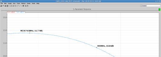
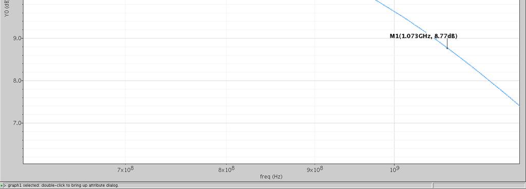
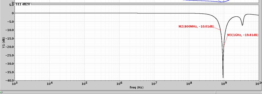
4 3. Simulation Results Fig1.2 Simulation Result for S21 Fig1.3 Simulation Result for S11
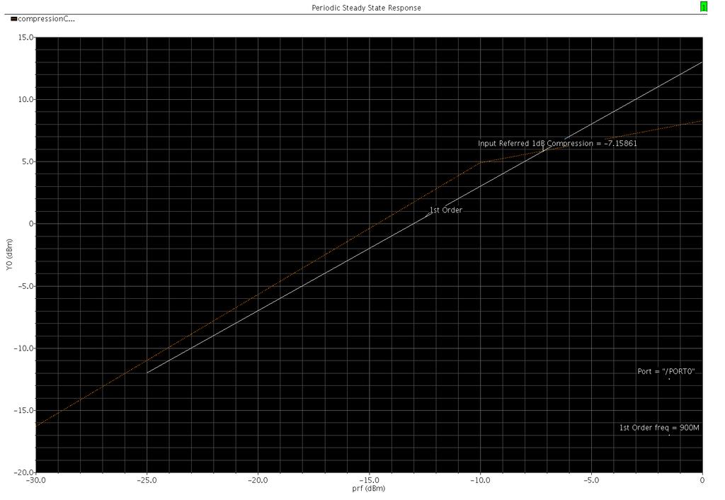
5 Fig1.4 Simulation Result for Noise Figure Fig1.5 Simulation Result for P1dB
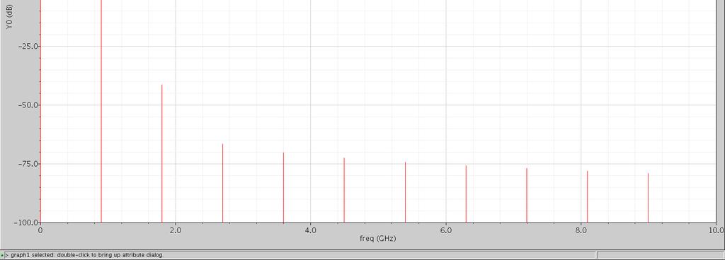
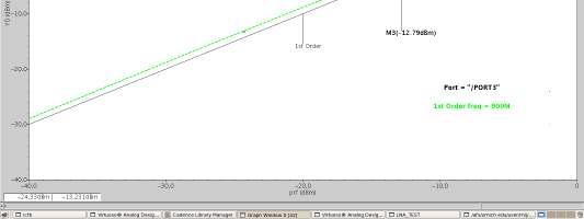
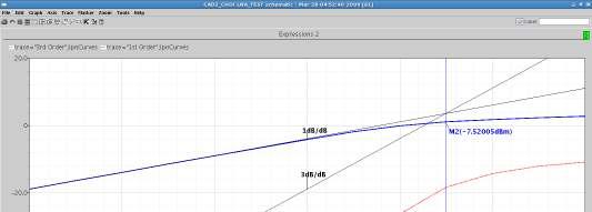
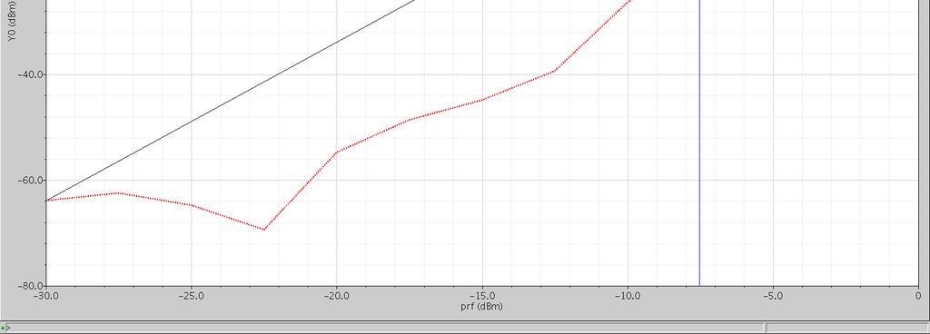
6 Fig1.6 Simulation Result for IIP3 (Start point = -10dBm) Fig1.6 Simulation Result for IIP3 (Start point = -28dBm)
7 CAD II: Low- oise Amplifier Design I. Device parameter summary Inductors Locations Value Outer diameter # of Turns gate inductance nh 1.64 mm 2 source degen nh 410 um 2 load inductance nh 10 mm 2 Capacitor (for C GS compensation) Location Value X dimension Y dimension Cgs compensation nh 1.64 mm 2 MOSFET Location Width Length #r of fingers Input 200 um 0.14 um 1 II. Simulation Results Parameters Result Peak S21 (Gain) db 3 db BW 797 MHz Center Freq MHz S db Noise Figure < db P1 db dbm IIP db Power Consumption 3.66 mw - 1 -
8 Schematic - 2 -

9 S21 (PSS) - 3 -

10 NF & S11-4 -

11 P1dB - 5 -
12 IIP3-6 -
13 Figure 1. NF, S11, S21
14 Figure2. 1dB Compression point.
15 Figure 3. 3dB Compression point.
16 Specification Desired Achieved Peak S21 Gain >10dB 15dB 3dB Bandwidth 200MHz 300MHz 500MHz to 1.028GHz Center Frequency 900MHz 763MHz (for peak Gain) ~900MHz (for NF) Noise Figure <1.7dB 1.25dB 1.31dB S11 < 10dB 10.2dB P1dB > 30dB 8.04dB IIP3 > 15dB 1.113dB Power Consumption < 4mW 3.8mW Table 1. Desired vs. Achieved values
17

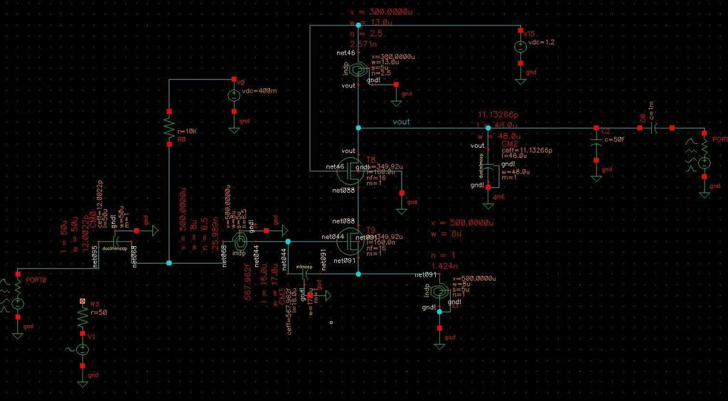
18 EECS 522 CAD2 1. Schematic of the LNA V dd = 1.2V V bias = 325 mv 1.63 nh turns = 1.5 Dimention = 380µm 17pF 60µm x 60.59µm 1µF c 12pF 50µm x 49.99µm 10KΩ W/L = 510µm 320nm 50fF Input port c nh turns = 2.5 Dimention = 1340µm W/L = 510µm 320nm 946 ph turns = 1 Dimention = 390µm Output port
 S11 < 10 db from 800 MHz to 1 GHz < 10.03 db (in band) P1dB > 30 dbm 1.57 dbm IIP3 > 15 dbm 8.15 dbm Power < 4 mw 3.924 mw Path: /afs/umich.edu/user/k/k/kkhuang/eecs522/cad/cad_lna 3.")
19 2. Summary Table Specification LNA Design Peak S21 > 10 db 12.4 db 3dB Bandwidth 200 MHz ~ 300 MHz 242 MHz Center Frequency 900 MHz 880 MHz Noise Figure < 1.7 db from 800 MHz to 1 GHz < 1.69 db (in band) S11 < 10 db from 800 MHz to 1 GHz < db (in band) P1dB > 30 dbm 1.57 dbm IIP3 > 15 dbm 8.15 dbm Power < 4 mw mw Path: /afs/umich.edu/user/k/k/kkhuang/eecs522/cad/cad_lna 3. Plots of S 11 S 21 P 1dB IIP 3 and Noise Figure
20
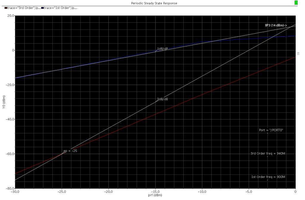
21 EECS522 CAD 2 Submitted March 28, 2009 TABLE OF MEASURED VALUES AND SPECIFICATIONS Specification Required This LNA Peak S21 (Gain) > 10 db db 3dB Bandwidth 200 MHz < BW <300 MHz MHz Center Frequency 900 MHz MHz Noise Figure S11 < 1.7 db between 800 MHz and 1 GHz db max < -10 db between 800 MHz and 1 GHz db max P1dB > -30 dbm (input feferred) db IIP3 > -15 dbm (input referred) 14 dbm Power Consumption < 4mW (including bias circuits) mw* * 3.31 ma is drawn from the 1.2 V supply by the transistors, the bias resistor contribution is negligible (~5 pw) Attached (in order): Illustration of the schematic Plots S11 S21 P1dB IIP3 Noise Figure
22
23
24
25
26
27
28 Specification Goal Simulation Results S21(Gain) >10 db >13 db 3db Bandwidth 200 MHz < BW <300 MHz 283 MHz Center Frequency 900 MHz 900 MHz Noise Figure <1.7 db between 800MHz & 1GHz <1.6 db between 800MHz & 1GHz S11 <-10 db between 800 MHz & 1 GHz <-10 db between 800 MHz & 1 GHz P1dB >-30 dbm input referred -8.3 dbm IIP3 >-15 dbm input referred -4.4 dbm Power Consumption <4mW 3.87 mw
29
30
31 Schematic The bias voltage was set to VDC.
32 Summary Peak S21 3dB BW IIP3 1 db Power Compression Design db MHz dbm mw Goal > 10 db 200 MHz < BW < 300 MHz > -15 dbm >-30 dbm < 4 mw Frequency S21 NF S MHz db db db 900 MHz db db db 1 GHz db db db Plots
33
34
35 Table 1 - Specification List EECS 522 3/27/09 Specification Target Value Actual Value Actual Value Actual Value Lower Corner 900MHz Upper Corner Peak S21 > 10dB db db db 3dB BW 200MHz < BW < 300MHz N/A 450 MHz N/A Center Frequency 900MHz N/A 900 MHz N/A Noise Figure <1.7dB between 800MHz db db db and 1GHz S11 <10dB between 800MHz db db db and 1GHz P1dB > -30dBm N/A dbm N/A IIP3 > -15dBm N/A dbm N/A Power Consumption < 4mW N/A mw N/A Table 2 - Component List Component Parameters Capacitance Length Width CM2 Capacitor fF 8.5um 11.05um CM1 Capacitor fF 8.5um 81.71um Inductance Outer Dimension n turns I3 Inductor nH 400um 8 I4 Inductor 1.609nH 150um 3 I5 Inductor 4.673nH 300um 3 Width Length # fingers T1 NFET 200um 150nm 8 T6 NFET 200um 150nm 8
36 EECS 522 3/27/09
37 EECS 522 3/27/09
38 EECS 522 3/27/09
39
40 figure 4 designed circuit
41 figure 5 s parameter analysis results ( s11)
42 figure 6 s parameter analysis results ( s21)
43 figure 7 s parameter analysis results (Noise Factor)
44 figure 6 1 db compression point
45 figure 7 IIP3 Point (it is -3.9 dbm, red line is 3th harmonic blue is fundamental)
46 EECS 522 CAD 2 EECS 522 CAD Assignment #2 Device Values and Sizes: Given Devices: R S = 50 Ω R bias = 10 k Ω C C = 12 pf C L = 50 ff V DD = 1.2 V V bias = 397 mv Figure 1. Schematic of 900 MHz LNA Including Given Components

47 Inductors: Inductance Outer Diameter Metal Width Number of Turns LG nh 470 µm 11 µm 7.5 LS nh 400 µm 10 µm 1 LD nh 290 µm 15 µm 2.5 Capacitors: Capacitance X Dimension Y Dimension CX ff 50 µm 6.75 µm CD pf 200 µm µm Transistors: Width of Single Finger Width of All Fingers Number of Fingers Length M µm µm 160 nm 25 M µm µm 160 nm 25 Summary Table:
48 Plots: Figure 2. Plot of S11 Figure 3. Plot of S21
49 Figure 4. Plot of P1dB Figure 5. Plot of IIP3
50 Figure 6. Plot of Noise Figure
Low Noise Amplifier Design
 THE UNIVERSITY OF TEXAS AT DALLAS DEPARTMENT OF ELECTRICAL ENGINEERING EERF 6330 RF Integrated Circuit Design (Spring 2016) Final Project Report on Low Noise Amplifier Design Submitted To: Dr. Kenneth
CHAPTER 4 ULTRA WIDE BAND LOW NOISE AMPLIFIER DESIGN
 93 CHAPTER 4 ULTRA WIDE BAND LOW NOISE AMPLIFIER DESIGN 4.1 INTRODUCTION Ultra Wide Band (UWB) system is capable of transmitting data over a wide spectrum of frequency bands with low power and high data
Texas A&M University Electrical Engineering Department ECEN 665. Laboratory #3: Analysis and Simulation of a CMOS LNA
 Texas A&M University Electrical Engineering Department ECEN 665 Laboratory #3: Analysis and Simulation of a CMOS LNA Objectives: To learn the use of s-parameter and periodic steady state (pss) simulation
Course Project Topic: RF Down-Conversion Chain Due Dates: Mar. 24, Apr. 7 (Interim reports), Apr. 28 (Final report)
, Apr. 28 (Final report)") Course Project Topic: RF Down-Conversion Chain Due Dates: Mar. 24, Apr. 7 (Interim reports), Apr. 28 (Final report) 1 Objective The objective of this project is to familiarize the student with the trade-offs
Course Project Topic: RF Down-Conversion Chain Due Dates: Mar. 24, Apr. 7 (Interim reports), Apr. 28 (Final report) 1 Objective The objective of this project is to familiarize the student with the trade-offs
Design of a Low Noise Amplifier using 0.18µm CMOS technology
 The International Journal Of Engineering And Science (IJES) Volume 4 Issue 6 Pages PP.11-16 June - 2015 ISSN (e): 2319 1813 ISSN (p): 2319 1805 Design of a Low Noise Amplifier using 0.18µm CMOS technology
AVoltage Controlled Oscillator (VCO) was designed and
 was designed and") 1 EECE 457 VCO Design Project Jason Khuu, Erik Wu Abstract This paper details the design and simulation of a Voltage Controlled Oscillator using a 0.13µm process. The final VCO design meets all specifications.
1 EECE 457 VCO Design Project Jason Khuu, Erik Wu Abstract This paper details the design and simulation of a Voltage Controlled Oscillator using a 0.13µm process. The final VCO design meets all specifications.
Quiz2: Mixer and VCO Design
 Quiz2: Mixer and VCO Design Fei Sun and Hao Zhong 1 Question1 - Mixer Design 1.1 Design Criteria According to the specifications described in the problem, we can get the design criteria for mixer design:
High IP3 Low-Noise Amplifier
 EVALUATION KIT AVAILABLE General Description The low-cost, high third-order intercept point (IP3) low-noise amplifier (LNA) is designed for applications in 2.4GHz WLAN, ISM, and Bluetooth radio systems.
ABabcdfghiejklStanford University
 Design Methodology or Power-Constrained Low Noise RF Circuits Jung-Suk Goo, Hee-Tae Ahn, Donald J Ladwig, Zhiping Yu, Thomas H Lee, and Robert W Dutton, Stanord University, Stanord CA National Semiconductor,
Designing a 960 MHz CMOS LNA and Mixer using ADS. EE 5390 RFIC Design Michelle Montoya Alfredo Perez. April 15, 2004
 Designing a 960 MHz CMOS LNA and Mixer using ADS EE 5390 RFIC Design Michelle Montoya Alfredo Perez April 15, 2004 The University of Texas at El Paso Dr Tim S. Yao ABSTRACT Two circuits satisfying the
RF CMOS 0.5 µm Low Noise Amplifier and Mixer Design
 RF CMOS 0.5 µm Low Noise Amplifier and Mixer Design By VIKRAM JAYARAM, B.Tech Signal Processing and Communication Group & UMESH UTHAMAN, B.E Nanomil FINAL PROJECT Presented to Dr.Tim S Yao of Department
Preliminary Exam, Fall 2013 Department of Electrical and Computer Engineering University of California, Irvine EECS 170B
 Preliminary Exam, Fall 2013 Department of Electrical and Computer Engineering University of California, Irvine EECS 170B Problem 1. Consider the following circuit, where a saw-tooth voltage is applied
DESIGN OF 3 TO 5 GHz CMOS LOW NOISE AMPLIFIER FOR ULTRA-WIDEBAND (UWB) SYSTEM
 SYSTEM") Progress In Electromagnetics Research C, Vol. 9, 25 34, 2009 DESIGN OF 3 TO 5 GHz CMOS LOW NOISE AMPLIFIER FOR ULTRA-WIDEBAND (UWB) SYSTEM S.-K. Wong and F. Kung Faculty of Engineering Multimedia University
Progress In Electromagnetics Research C, Vol. 9, 25 34, 2009 DESIGN OF 3 TO 5 GHz CMOS LOW NOISE AMPLIFIER FOR ULTRA-WIDEBAND (UWB) SYSTEM S.-K. Wong and F. Kung Faculty of Engineering Multimedia University
Texas A&M University Electrical Engineering Department ECEN 665. Laboratory #4: Analysis and Simulation of a CMOS Mixer
 Texas A&M University Electrical Engineering Department ECEN 665 Laboratory #4: Analysis and Simulation of a CMOS Mixer Objectives: To learn the use of periodic steady state (pss) simulation tools in spectre
95GHz Receiver with Fundamental Frequency VCO and Static Frequency Divider in 65nm Digital CMOS
 95GHz Receiver with Fundamental Frequency VCO and Static Frequency Divider in 65nm Digital CMOS Ekaterina Laskin, Mehdi Khanpour, Ricardo Aroca, Keith W. Tang, Patrice Garcia 1, Sorin P. Voinigescu University
Aspemyr, Lars; Jacobsson, Harald; Bao, Mingquan; Sjöland, Henrik; Ferndal, Mattias; Carchon, G
 A 15 GHz and a 2 GHz low noise amplifier in 9 nm RF CMOS Aspemyr, Lars; Jacobsson, Harald; Bao, Mingquan; Sjöland, Henrik; Ferndal, Mattias; Carchon, G Published in: Topical Meeting on Silicon Monolithic
HIGH-GAIN CMOS LOW NOISE AMPLIFIER FOR ULTRA WIDE-BAND WIRELESS RECEIVER
 Progress In Electromagnetics Research C, Vol. 7, 183 191, 2009 HIGH-GAIN CMOS LOW NOISE AMPLIFIER FOR ULTRA WIDE-BAND WIRELESS RECEIVER A. Dorafshan and M. Soleimani Electrical Engineering Department Iran
IF Digitally Controlled Variable-Gain Amplifier
 19-2601; Rev 1; 2/04 IF Digitally Controlled Variable-Gain Amplifier General Description The high-performance, digitally controlled variable-gain amplifier is designed for use from 0MHz to 400MHz. The
Design of a Low Power 5GHz CMOS Radio Frequency Low Noise Amplifier Rakshith Venkatesh
 Design of a Low Power 5GHz CMOS Radio Frequency Low Noise Amplifier Rakshith Venkatesh Abstract A 5GHz low power consumption LNA has been designed here for the receiver front end using 90nm CMOS technology.
CHAPTER 3 CMOS LOW NOISE AMPLIFIERS
 46 CHAPTER 3 CMOS LOW NOISE AMPLIFIERS 3.1 INTRODUCTION The Low Noise Amplifier (LNA) plays an important role in the receiver design. LNA serves as the first block in the RF receiver. It is a critical
ATF High Intercept Low Noise Amplifier for the MHz PCS Band using the Enhancement Mode PHEMT
 ATF-54143 High Intercept Low Noise Amplifier for the 185 191 MHz PCS Band using the Enhancement Mode PHEMT Application Note 1222 Introduction Avago Technologies ATF-54143 is a low noise enhancement mode
Course Project Topic: RF Down-Conversion Chain Due Dates: Mar. 27, Apr. 15 (Interim reports), May. 11 (Final report)
, May. 11 (Final report)") Course Project Topic: RF Down-Conversion Chain Due Dates: Mar. 27, Apr. 15 (Interim reports), May. 11 (Final report) 1 Objective The objective of this project is to familiarize the student with the trade-offs
Course Project Topic: RF Down-Conversion Chain Due Dates: Mar. 27, Apr. 15 (Interim reports), May. 11 (Final report) 1 Objective The objective of this project is to familiarize the student with the trade-offs
1-13GHz Wideband LNA utilizing a Transformer as a Compact Inter-stage Network in 65nm CMOS
 -3GHz Wideband LNA utilizing a Transformer as a Compact Inter-stage Network in 65nm CMOS Hyohyun Nam and Jung-Dong Park a Division of Electronics and Electrical Engineering, Dongguk University, Seoul E-mail
DESIGN AND ANALYSIS OF 2 GHz 130nm CMOS CASCODE LOW NOISE AMPLIFIER WITH INTEGRATED CIRCULARLY POLARIZED PATCH ANTENNA
 DESIGN AND ANALYSIS OF 2 GHz 130nm CMOS CASCODE LOW NOISE AMPLIFIER WITH INTEGRATED CIRCULARLY POLARIZED PATCH ANTENNA Varun D. 1 1 Department of Electronics and Electrical Engineering, M. S. Ramaiah School
MGA Low Noise Amplifier. Data Sheet. Features. Description. Applications. Surface Mount Package SOT-343 /4-lead SC70. Simplified Schematic
 MGA-243 Low Noise Amplifier Data Sheet Description Avago Technologies MGA-243 is an economical, easyto-use GaAs MMIC Low Noise Amplifier (LNA), which is designed for use in LNA and driver stages. While
Application Note 1299
 A Low Noise High Intercept Point Amplifier for 9 MHz Applications using ATF-54143 PHEMT Application Note 1299 1. Introduction The Avago Technologies ATF-54143 is a low noise enhancement mode PHEMT designed
SP 22.3: A 12mW Wide Dynamic Range CMOS Front-End for a Portable GPS Receiver
 SP 22.3: A 12mW Wide Dynamic Range CMOS Front-End for a Portable GPS Receiver Arvin R. Shahani, Derek K. Shaeffer, Thomas H. Lee Stanford University, Stanford, CA At submicron channel lengths, CMOS is
ENGDA Wideband Distributed Amplifier, DIE, 0.8 to 20 GHz ENGDA Features. Typical Applications. Description. Functional Block Diagram
 Typical Applications ENGDA00072 Wideband Distributed Amplifier, DIE, 0.8 to 20 GHz ENGDA00072 Features Military EW and SIGINT Receiver or Transmitter Telecom Infrastructure Space Hybrids Test and Measurement
Maxim > Design Support > Technical Documents > Application Notes > Wireless and RF > APP 3571
 Maxim > Design Support > Technical Documents > Application Notes > Wireless and RF > APP 3571 Keywords: automotive keyless entry, MAX2640, LNA, 315MHz, RKE, stability, automotive, keyless entry APPLICATION
High Gain Low Noise Amplifier Design Using Active Feedback
 Chapter 6 High Gain Low Noise Amplifier Design Using Active Feedback In the previous two chapters, we have used passive feedback such as capacitor and inductor as feedback. This chapter deals with the
Features. Gain: 14.5 db. Electrical Specifications [1] [2] = +25 C, Rbias = 825 Ohms for Vdd = 5V, Rbias = 5.76k Ohms for Vdd = 3V
![Features. Gain: 14.5 db. Electrical Specifications [1] [2] = +25 C, Rbias = 825 Ohms for Vdd = 5V, Rbias = 5.76k Ohms for Vdd = 3V](/thumbs/90/101370216.jpg "Features. Gain: 14.5 db. Electrical Specifications [1] [2] = +25 C, Rbias = 825 Ohms for Vdd = 5V, Rbias = 5.76k Ohms for Vdd = 3V") Typical Applications The HMC77ALP3E is ideal for: Fixed Wireless and LTE/WiMAX/4G BTS & Infrastructure Repeaters and Femtocells Public Safety Radio Access Points Functional Diagram Features Noise Figure:.
Typical Applications The HMC77ALP3E is ideal for: Fixed Wireless and LTE/WiMAX/4G BTS & Infrastructure Repeaters and Femtocells Public Safety Radio Access Points Functional Diagram Features Noise Figure:.
James Lunsford HW2 2/7/2017 ECEN 607
 James Lunsford HW2 2/7/2017 ECEN 607 Problem 1 Part A Figure 1: Negative Impedance Converter To find the input impedance of the above NIC, we use the following equations: V + Z N V O Z N = I in, V O kr
LNAs with Step Attenuator and VGA
 19-231; Rev 1; 1/6 EVALUATION KIT AVAILABLE LNAs with Step Attenuator and VGA General Description The wideband low-noise amplifier (LNA) ICs are designed for direct conversion receiver (DCR) or very low
LINEARITY IMPROVEMENT OF CASCODE CMOS LNA USING A DIODE CONNECTED NMOS TRANSISTOR WITH A PARALLEL RC CIRCUIT
 Progress In Electromagnetics Research C, Vol. 17, 29 38, 2010 LINEARITY IMPROVEMENT OF CASCODE CMOS LNA USING A DIODE CONNECTED NMOS TRANSISTOR WITH A PARALLEL RC CIRCUIT C.-P. Chang, W.-C. Chien, C.-C.
MCP to 2.5 GHz RF Front End IC. Description
 Description The contains a power amplifier (PA), a low noise amplifier (LNA), and two SPDT switch. It is a 0-pins IC by 4 4mm -QFN package. RF input and output impedance of are 50Ω matched. Therefore,
A 5.2GHz RF Front-End
 University of Michigan, EECS 522 Final Project, Winter 2011 Natekar, Vasudevan and Viswanath 1 A 5.2GHz RF Front-End Neel Natekar, Vasudha Vasudevan, and Anupam Viswanath, University of Michigan, Ann Arbor.
ETI , Good luck! Written Exam Integrated Radio Electronics. Lund University Dept. of Electroscience
 und University Dept. of Electroscience EI170 Written Exam Integrated adio Electronics 2010-03-10, 08.00-13.00 he exam consists of 5 problems which can give a maximum of 6 points each. he total maximum
Signal Integrity Design of TSV-Based 3D IC
 Signal Integrity Design of TSV-Based 3D IC October 24, 21 Joungho Kim at KAIST joungho@ee.kaist.ac.kr http://tera.kaist.ac.kr 1 Contents 1) Driving Forces of TSV based 3D IC 2) Signal Integrity Issues
A 900 MHz CMOS RF Receiver
 ECE 524, Yeu Kwak and Johannes Grad: A 900 MHz CMOS Receiver 1 A 900 MHz CMOS RF Receiver Illinois Institute of Technology ECE 524 Project Spring 2002 Yeu Kwak and Johannes Grad Abstract A radio frequency
Application Note 5038
 MGA-6P8 Buffer Amplifier for 10 MHz Application Application Note 038 Introduction The MGA-6P8 is a high isolation buffer amplifier based on Avago Technologies EPHEMT process. This application note discusses
Application Note 5057
 A 1 MHz to MHz Low Noise Feedback Amplifier using ATF-4143 Application Note 7 Introduction In the last few years the leading technology in the area of low noise amplifier design has been gallium arsenide
7-12GHz LNA. GaAs Monolithic Microwave IC. S21 (db)
") S21 (db) NF (db) GaAs Monolithic Microwave IC Description The is a monolithic two-stages wide band low noise amplifier circuit. It is self-biased. It is designed for military, space and telecommunication
S21 (db) NF (db) GaAs Monolithic Microwave IC Description The is a monolithic two-stages wide band low noise amplifier circuit. It is self-biased. It is designed for military, space and telecommunication
A 16Ω Audio Amplifier with 93.8 mw Peak loadpower and 1.43 quiscent power consumption
 A 16Ω Audio Amplifier with 93.8 mw Peak loadpower and 1.43 quiscent power consumption IEEE Transactions on circuits and systems- Vol 59 No:3 March 2012 Abstract A class AB audio amplifier is used to drive
Dual-band LNA Design for Wireless LAN Applications. 2.4 GHz LNA 5 GHz LNA Min Typ Max Min Typ Max
 Dual-band LNA Design for Wireless LAN Applications White Paper By: Zulfa Hasan-Abrar, Yut H. Chow Introduction Highly integrated, cost-effective RF circuitry is becoming more and more essential to the
Quadrature GPS Receiver Front-End in 0.13μm CMOS: The QLMV cell
 1 Quadrature GPS Receiver Front-End in 0.13μm CMOS: The QLMV cell Yee-Huan Ng, Po-Chia Lai, and Jia Ruan Abstract This paper presents a GPS receiver front end design that is based on the single-stage quadrature
Wide-Band Two-Stage GaAs LNA for Radio Astronomy
 Progress In Electromagnetics Research C, Vol. 56, 119 124, 215 Wide-Band Two-Stage GaAs LNA for Radio Astronomy Jim Kulyk 1,GeWu 2, Leonid Belostotski 2, *, and James W. Haslett 2 Abstract This paper presents
Dual-Frequency GNSS Front-End ASIC Design
 Dual-Frequency GNSS Front-End ASIC Design Ed. 01 15/06/11 In the last years Acorde has been involved in the design of ASIC prototypes for several EU-funded projects in the fields of FM-UWB communications
Multimode 2.4 GHz Front-End with Tunable g m -C Filter. Group 4: Nick Collins Trevor Hunter Joe Parent EECS 522 Winter 2010
 Multimode 2.4 GHz Front-End with Tunable g m -C Filter Group 4: Nick Collins Trevor Hunter Joe Parent EECS 522 Winter 2010 Overview Introduction Complete System LNA Mixer Gm-C filter Conclusion Introduction
65-nm CMOS, W-band Receivers for Imaging Applications
 65-nm CMOS, W-band Receivers for Imaging Applications Keith Tang Mehdi Khanpour Patrice Garcia* Christophe Garnier* Sorin Voinigescu University of Toronto, *STMicroelectronics University of Toronto 27
DESCRIPTIO FEATURES APPLICATIO S. LT GHz to 2.7GHz Receiver Front End TYPICAL APPLICATIO
 1.GHz to 2.GHz Receiver Front End FEATURES 1.V to 5.25V Supply Dual LNA Gain Setting: +13.5dB/ db at Double-Balanced Mixer Internal LO Buffer LNA Input Internally Matched Low Supply Current: 23mA Low Shutdown
50 GHz to 95 GHz, GaAs, phemt, MMIC, Wideband Power Amplifier ADPA7001CHIPS
 FEATURES Gain:.5 db typical at 5 GHz to 7 GHz S11: db typical at 5 GHz to 7 GHz S: 19 db typical at 5 GHz to 7 GHz P1dB: 17 dbm typical at 5 GHz to 7 GHz PSAT: 1 dbm typical OIP3: 5 dbm typical at 7 GHz
LAB-2 (Tutorial) Simulation of LNA (Cadence SpectreRF)
 Simulation of LNA (Cadence SpectreRF)") Spring 2006: RF CMOS Transceiver Design (TSEK-26) 1/18 Date: Student Name: Lab Supervisor: Personal Number: - Signature: Notes: LAB-2 (Tutorial) Simulation of LNA (Cadence SpectreRF) Prepared By Rashad.M.Ramzan
Spring 2006: RF CMOS Transceiver Design (TSEK-26) 1/18 Date: Student Name: Lab Supervisor: Personal Number: - Signature: Notes: LAB-2 (Tutorial) Simulation of LNA (Cadence SpectreRF) Prepared By Rashad.M.Ramzan
Application Note 1285
 Low Noise Amplifiers for 5.125-5.325 GHz and 5.725-5.825 GHz Using the ATF-55143 Low Noise PHEMT Application Note 1285 Description This application note describes two low noise amplifiers for use in the
A 2.4 GHZ RECEIVER IN SILICON-ON-SAPPHIRE MICHAEL PETERS. B.S., Kansas State University, 2009 A REPORT
 A 2.4 GHZ RECEIVER IN SILICON-ON-SAPPHIRE by MICHAEL PETERS B.S., Kansas State University, 2009 A REPORT submitted in partial fulfillment of the requirements for the degree MASTER OF SCIENCE Department
30 MHz to 6 GHz RF/IF Gain Block ADL5611
 Data Sheet FEATURES Fixed gain of 22.2 db Broad operation from 3 MHz to 6 GHz High dynamic range gain block Input and output internally matched to Ω Integrated bias circuit OIP3 of 4. dbm at 9 MHz P1dB
MGA Low Noise Amplifier. Data Sheet. 42x. Features. Description. Applications. Surface Mount Package SOT-343 /4-lead SC70. Simplified Schematic
 MGA-243 Low Noise Amplifier Data Sheet Description Avago Technologies MGA-243 is an economical, easyto-use GaAs MMIC Low Noise Amplifier (LNA), which is designed for use in LNA and driver stages. While
FD-SOI FOR RF IC DESIGN. SITRI LETI Workshop Mercier Eric 08 september 2016
 FD-SOI FOR RF IC DESIGN SITRI LETI Workshop Mercier Eric 08 september 2016 UTBB 28 nm FD-SOI : RF DIRECT BENEFITS (1/2) 3 back-end options available Routing possible on the AluCap level no restriction
50 MHz to 4.0 GHz RF/IF Gain Block ADL5602
 Data Sheet FEATURES Fixed gain of 20 db Operation from 50 MHz to 4.0 GHz Highest dynamic range gain block Input/output internally matched to 50 Ω Integrated bias control circuit OIP3 of 42.0 dbm at 2.0
Homework Assignment 11
 Homework Assignment 11 Question 1 (Short Takes) Two points each unless otherwise indicated. 1. What is the 3-dB bandwidth of the amplifier shown below if r π = 2.5K, r o = 100K, g m = 40 ms, and C L =
MD3880DB1: Ultrasound Low Noise Amplifier Demoboard
 MD388DB1: Ultrasound Low Noise Amplifier Demoboard MD388DB1 General Description The MD388DB1 demoboard is a platform for testing and evaluating the MD388 4-channel low-noise amplifi er (LNA) with a variable
30 MHz to 6 GHz RF/IF Gain Block ADL5544
 Data Sheet FEATURES Fixed gain of 17.4 db Broadband operation from 3 MHz to 6 GHz Input/output internally matched to Ω Integrated bias control circuit OIP3 of 34.9 dbm at 9 MHz P1dB of 17.6 dbm at 9 MHz
Application Note No. 075
 Application Note, Rev. 2.0, Jan. 2007 Application Note No. 075 High Third-Order Input Intercept Point CDMA 800 Low Noise Amplifier RF & Protection Devices Edition 2007-01-08 Published by Infineon Technologies
Single stage LNA for GPS Using the MCH4009 Application Note
 Single stage LNA for GPS Using the MCH49 Application Note http://onsemi.com Overview This application note explains about ON Semiconductor s MCH49 which is used as a Low Noise Amplifier (LNA) for GPS (Global
CMY210. Demonstration Board Documentation / Applications Note (V1.0) Ultra linear General purpose up/down mixer 1. DESCRIPTION
 Ultra linear General purpose up/down mixer 1. DESCRIPTION") Demonstration Board Documentation / (V1.0) Ultra linear General purpose up/down mixer Features: Very High Input IP3 of 24 dbm typical Very Low LO Power demand of 0 dbm typical; Wide input range Wide LO
Demonstration Board Documentation / (V1.0) Ultra linear General purpose up/down mixer Features: Very High Input IP3 of 24 dbm typical Very Low LO Power demand of 0 dbm typical; Wide input range Wide LO
PARAMETER CONDITIONS TYPICAL PERFORMANCE Operating Supply Voltage 3.1V to 3.5V Supply Current V CC = 3.3V, LO applied 152mA
 DESCRIPTION LT5578 Demonstration circuit 1545A-x is a high linearity upconverting mixer featuring the LT5578. The LT 5578 is a high performance upconverting mixer IC optimized for output frequencies in
30 MHz to 6 GHz RF/IF Gain Block ADL5610
 Data Sheet FEATURES Fixed gain of 18.4 db Broad operation from 3 MHz to 6 GHz High dynamic range gain block Input and output internally matched to Ω Integrated bias circuit OIP3 of 38.8 dbm at 9 MHz P1dB
0.5-4GHz Low Noise Amplifier
 .5-4GHz Low Noise Amplifier Features Frequency Range:.5-4 GHz Better than 2.dB Noise Figure Single supply operation db Nominal Gain dbm Nominal P1dB Input Return Loss > db Output Return Loss > db DC decoupled
High-Linearity CMOS. RF Front-End Circuits
 High-Linearity CMOS RF Front-End Circuits Yongwang Ding Ramesh Harjani iigh-linearity CMOS tf Front-End Circuits - Springer Library of Congress Cataloging-in-Publication Data A C.I.P. Catalogue record
0.5-4GHz Low Noise Amplifier
 ASL P3.5-4GHz Low Noise Amplifier Features Frequency Range:.5-4 GHz Better than 2.dB Noise Figure Single supply operation db Nominal Gain dbm Nominal P1dB Input Return Loss > db Output Return Loss > db
RF9986. Micro-Cell PCS Base Stations Portable Battery Powered Equipment
 RF996 CDMA/TDMA/DCS900 PCS Systems PHS 500/WLAN 2400 Systems General Purpose Down Converter Micro-Cell PCS Base Stations Portable Battery Powered Equipment The RF996 is a monolithic integrated receiver
CMOS Dual Band Receiver GSM 900-Mhz / DSS-GSM1800-GHz
 CMOS Dual Band Receiver GSM 900-Mhz / DSS-GSM1800-GHz By : Dhruvang Darji 46610334 Transistor integrated Circuit A Dual-Band Receiver implemented with a weaver architecture with two frequency stages operating
LF to 4 GHz High Linearity Y-Mixer ADL5350
 LF to GHz High Linearity Y-Mixer ADL535 FEATURES Broadband radio frequency (RF), intermediate frequency (IF), and local oscillator (LO) ports Conversion loss:. db Noise figure:.5 db High input IP3: 25
CIRF Circuit Intégré Radio Fréquence. Low Noise Amplifier. Delaram Haghighitalab Hassan Aboushady Université Paris VI
 CIRF Circuit Intégré Radio Fréquence Low Noise Amplifier Delaram Haghighitalab Hassan Aboushady Université Paris VI Multidisciplinarity of radio design H. Aboushady University of Paris VI References M.
Introduction to Surface Acoustic Wave (SAW) Devices
 Devices") May 31, 2018 Introduction to Surface Acoustic Wave (SAW) Devices Part 7: Basics of RF Circuits Ken-ya Hashimoto Chiba University k.hashimoto@ieee.org http://www.te.chiba-u.jp/~ken Contents Noise Figure
May 31, 2018 Introduction to Surface Acoustic Wave (SAW) Devices Part 7: Basics of RF Circuits Ken-ya Hashimoto Chiba University k.hashimoto@ieee.org http://www.te.chiba-u.jp/~ken Contents Noise Figure
400 MHz 4000 MHz Low Noise Amplifier ADL5521
 FEATURES Operation from 400 MHz to 4000 MHz Noise figure of 0.8 db at 900 MHz Including external input match Gain of 20.0 db at 900 MHz OIP3 of 37.7 dbm at 900 MHz P1dB of 22.0 dbm at 900 MHz Integrated
CGY2107HV CGY2107HV PRODUCT DATASHEET. Dual High Gain Low Noise High IP3 Amplifier. Rev 0.2 FEATURES APPLICATIONS DESCRIPTION
 Rev 0.1 PRODUCT DATASHEET Dual High Gain Low Noise High IP3 Amplifier DESCRIPTION The is an extremely Low Noise cascode Amplifier with state of the art Noise Figure and Linearity suitable for applications
A 2.4-Ghz Differential Low-noise Amplifiers using 0.18um CMOS Technology
 International Journal of Electronic and Electrical Engineering. ISSN 0974-2174, Volume 7, Number 3 (2014), pp. 207-212 International Research Publication House http://www.irphouse.com A 2.4-Ghz Differential
EECS 290C: Advanced circuit design for wireless Class Final Project Due: Thu May/02/2019
 EECS 290C: Advanced circuit design for wireless Class Final Project Due: Thu May/02/2019 Project: A fully integrated 2.4-2.5GHz Bluetooth receiver. The receiver has LNA, RF mixer, baseband complex filter,
A 3 5 GHz CMOS High Linearity Ultra Wideband Low Noise Amplifier in 0.18µ CMOS
 Proceedings of the 5th WSEAS Int. Conf. on CIRCUITS, SYSTEMS, ELECTRONICS, CONTROL & SIGNAL PROCESSING, Dallas, USA, November -, 6 5 A 5 GHz CMOS High Linearity Ultra Wideband Low Noise Amplifier in.8µ
RF OUT / N/C RF IN / V G
 MAAM-111 MHz - 2 GHz Rev. V2 Features Functional Schematic 12 db Gain Ω Input / Output Match over Gain Range 3 db Gain Control with to -2 V Control +18 dbm Output Power + V, -. V DC, 7 ma Lead-Free 1.
Designing of Low Power RF-Receiver Front-end with CMOS Technology
 Sareh Salari Shahrbabaki Designing of Low Power RF-Receiver Front-end with CMOS Technology School of Electrical Engineering Thesis submitted for examination for the degree of Master of Science in Technology.
30% PAE W-band InP Power Amplifiers using Sub-quarter-wavelength Baluns for Series-connected Power-combining
 2013 IEEE Compound Semiconductor IC Symposium, October 13-15, Monterey, C 30% PAE W-band InP Power Amplifiers using Sub-quarter-wavelength Baluns for Series-connected Power-combining 1 H.C. Park, 1 S.
Features. = +25 C, IF = 200 MHz, LO = 0 dbm, Vcc = Vcc1, 2, 3 = +5V, G_Bias = +2.5V*
 v4.1 Typical Applications The HMC685LP4(E) is Ideal for: Cellular/3G & LTE/WiMAX/4G Basestations & Repeaters GSM, CDMA & OFDM Transmitters and Receivers Features High Input IP3: +35 dbm 8 db Conversion
Design technique of broadband CMOS LNA for DC 11 GHz SDR
 Design technique of broadband CMOS LNA for DC 11 GHz SDR Anh Tuan Phan a) and Ronan Farrell Institute of Microelectronics and Wireless Systems, National University of Ireland Maynooth, Maynooth,Co. Kildare,
An Asymmetrical Bulk CMOS Switch for 2.4 GHz Application
 Progress In Electromagnetics Research Letters, Vol. 66, 99 104, 2017 An Asymmetrical Bulk CMOS Switch for 2.4 GHz Application Lang Chen 1, * and Ye-Bing Gan 1, 2 Abstract A novel asymmetrical single-pole
UHF BAND LOW NOISE AMPLIFIER GaAs MMIC
 NJGHA UHF BAND LOW NOISE AMPLIFIER GaAs MMIC GENERAL DESCRIPTION NJGHA is a low noise amplifier GaAs MMIC designed for mobile digital TV application (~ MHz). This IC features good gain flatness, and low
Microelectronics Exercises of Topic 5 ICT Systems Engineering EPSEM - UPC
 Microelectronics Exercises of Topic 5 ICT Systems Engineering EPSEM - UPC F. Xavier Moncunill Autumn 2018 5 Analog integrated circuits Exercise 5.1 This problem aims to follow the steps in the design of
Application Note 5379
 VMMK-1225 Applications Information Application Note 5379 Introduction The Avago Technologies VMMK-1225 is a low noise enhancement mode PHEMT designed for use in low cost commercial applications in the
TSEK03 LAB 1: LNA simulation using Cadence SpectreRF
 TSEK03 Integrated Radio Frequency Circuits 2018/Ted Johansson 1/26 TSEK03 LAB 1: LNA simulation using Cadence SpectreRF Ver. 2018-09-18 for Cadence 6 & MMSIM 14 Receiver Front-end LO RF Filter 50W LNA
OBSOLETE HMC915LP4E. GaAs MMIC MIXER w/ INTEGRATED LO AMPLIFIER, GHz. Typical Applications. Features. Functional Diagram. General Description
 v1.5 LO AMPLIFIER,.5-2.7 GHz Typical Applications The is ideal for: PCS / 3G Infrastructure Base Stations & Repeaters WiMAX & WiBro ISM & Fixed Wireless Functional Diagram Features Input IP3: +28 dbm Low
Features OBSOLETE. = +25 C, Rbias = 0 Ohm. Bypass Mode Failsafe Mode Parameter
 7 Typical Applications The HMC668LP3(E) is ideal for: Cellular/3G and LTE/WiMAX/4G BTS & Infrastructure Repeaters and Femtocells Tower Mounted Amplifiers Test & Measurement Equipment Functional Diagram
0.85V. 2. vs. I W / L
 EE501 Lab3 Exploring Transistor Characteristics and Design Common-Source Amplifiers Lab report due on September 22, 2016 Objectives: 1. Be familiar with characteristics of MOSFET such as gain, speed, power,
Design and Implementation of a 1-5 GHz UWB Low Noise Amplifier in 0.18 um CMOS
 Downloaded from vbn.aau.dk on: marts 20, 2019 Aalborg Universitet Design and Implementation of a 1-5 GHz UWB Low Noise Amplifier in 0.18 um CMOS Shen, Ming; Tong, Tian; Mikkelsen, Jan H.; Jensen, Ole Kiel;
Features. Upconversion & Downconversion Applications MIXERS - SINGLE & DOUBLE BALANCED - SMT
 v1. Typical Applications The HMC688LP4(E) is Ideal for: Cellular/3G & LTE/WiMAX/4G Basestations & Repeaters GSM, CDMA & OFDM Transmitters and Receivers Features High Input IP3: +35 dbm Low Conversion Loss:
ESD Sensitive Component!!
 5 MHz LOW NOISE AMPLIFIER WHM3AE 1 REV E WHM3AE LNA is a low noise figure, wideband, and high linear SMT packaged amplifier with exceptional gain flatness design. The amplifier offers typical.7 db noise
RF2418 LOW CURRENT LNA/MIXER
 LOW CURRENT LNA/MIXER RoHS Compliant & Pb-Free Product Package Style: SOIC-14 Features Single 3V to 6.V Power Supply High Dynamic Range Low Current Drain High LO Isolation LNA Power Down Mode for Large
Low-Noise Amplifiers
 007/Oct 4, 31 1 General Considerations Noise Figure Low-Noise Amplifiers Table 6.1 Typical LNA characteristics in heterodyne systems. NF IIP 3 db 10 dbm Gain 15 db Input and Output Impedance 50 Ω Input
MAAL Low Noise Amplifier GHz. Features. Functional Block Diagram. Description. Pin Configuration 1. Ordering Information 2,3 N/C
 MAAL-4.1-3. GHz Features Single Voltage Supply 3V ~ V Integrated Active Bias Circuit Adjustable Current with an External Resistor Low Noise Figure High Linearity OIP3, 34 dbm @ 2 GHz Broadband Match Integrated
17-26GHz Medium Power Amplifier. GaAs Monolithic Microwave IC
 Description The CHA5050-99F is a four stage monolithic MPA that provides typically 25.5dBm of output power associated to 20% of power added efficiency at 3dB gain compression. It is designed for a wide
Features. Upconversion & Downconversion Applications MIXERS - SINGLE & DOUBLE BALANCED - SMT
 v1. Typical Applications The HMC689LP4(E) is Ideal for: Cellular/3G & LTE/WiMAX/4G Basestations & Repeaters GSM, CDMA & OFDM Transmitters and Receivers Features High Input IP3: +32 dbm Low Conversion Loss: