A 3.9 ns 8.9 mw 4 4 Silicon Photonic Switch Hybrid-Integrated with CMOS Driver
|
|
|
- Gwendoline Grace Parrish
- 5 years ago
- Views:
Transcription
1 A 3.9 ns 8.9 mw 4 4 Silicon Photonic Switch Hybrid-Integrated with CMOS Driver A. Rylyakov, C. Schow, B. Lee, W. Green, J. Van Campenhout, M. Yang, F. Doany, S. Assefa, C. Jahnes, J. Kash, Y. Vlasov IBM T.J. Watson Research Center, Yorktown Heights, NY
2 Outline Motivation Silicon photonics technology overview Integration strategies: full monolithic and hybrid 4 4 switch hybrid-integrated with CMOS driver Conclusion 2
3 Motivation Goal: develop photonic device process compatible with CMOS enables high-speed, high-density interconnects for lower power, lower cost, long reach communication opens up a number of new applications (biomedical, sensor, etc) Hybrid integration (flip-chip or wirebond) of Si photonic devices and electrical circuits: ideal for early prototyping important step towards full integration either hybrid or monolithically integrated could be commercialized A 4 4 switch requires the development of all key components, highlights the advantages of the silicon photonic technology: data stays in the optical domain multiple data streams routed in the same device (WDM) 3
4 Outline Motivation Silicon photonics technology overview: Waveguides ( SOI photonic wires ), other passive devices Modulators, detectors Fiber coupling Integration strategies: full monolithic and hybrid 4 4 switch hybrid-integrated with CMOS driver Conclusion 4
 2 µm thick buried oxide (BOX) Waveguide cross-section color-coded with intensity of electric field (λ =.")
 Si surrounded by SiO 2 forms a dielectric")
5 Silicon Photonic Waveguide.5 µm Si (n=3.5).2 µm SiO 2 (n=.45) 2 µm thick buried oxide (BOX) Waveguide cross-section color-coded with intensity of electric field (λ =.55 µm) Undoped Si and SiO 2 are transparent for λ =.2 µm 6.5 µm (this range covers the long haul optical communication C-band) Si surrounded by SiO 2 forms a dielectric waveguide (similar to single mode fiber, but much smaller due to high contrast ratio) Losses (2 µm BOX) : ~2 db/cm and ~. db/bend (R ~5 µm) 5
6 Y-junction: Silicon Photonic Passive Devices split merge Directional coupler: IN T.3 µm coupling length T 2 Ring resonator: IN THRU Ring resonator can be used as add/drop for WDM DROP 6
7 Mach-Zehnder Interferometer Based Modulator IN p-i-n diode phase shifter ON/OFF φ T P P OUT IN = + cos( φ) 2 T 2 5% directional couplers Mach-Zehnder interferometer (MZI) splits the signal into two arms, adds relative phase and then merges the arms again One MZI arm contains a p-i-n diode that implements an optical phase shift through charge injection 7

8 MZI Modulator with Integrated p-i-n Diode Cross section of one MZI arm shows the partially etched rib waveguide with p-i-n diode 5 µm p-i-n diode phase shifter (L = 2 µm) T IN 5% directional coupler 5 nm T 2 The p-i-n diode injects charge into the core of the waveguide, resulting in optical phase shift without significant loss of signal Cu NiSi Si 3 N 4 light charge Si Cu W p i n W. Green, et al. (27); J. Van Campenhout, et al. (29) 8


9 Waveguide Coupled Germanium Detector Cross section Performance: 4 Gb/s (at 2 V bias) Die photo Ge photodetector in CMOS compatible process Speed: 4 Gb/s Size: 2 µm long (~ ff ) Avalanche gain demonstrated at.5 V S.Assefa, et al. (Nature 2) 9
 SiON waveguide ( µm 3 µm) single mode fiber core (9 µm diameter) pitch mismatch: Y. Vlasov, et al.")
10 Edge Coupling to Standard Fiber SiON couplers over tapered Si waveguides help mitigate the cross-section mismatch: Si waveguide (.2 µm.5 µm) SiON waveguide ( µm 3 µm) single mode fiber core (9 µm diameter) pitch mismatch: Y. Vlasov, et al. (23) parallel fiber array (25 µm pitch) Si waveguide array (2 µm pitch)

 to Si waveguide B. G. Lee, et al.")
11 Optical Coupling to Parallel Waveguides: 64 Gb/s: 4λ in 4 waveguides at 4 Gb/s input 53 nm 537 nm 543 nm 549 nm WG WG 2 WG 3 WG 4 ps Multichannel tapered coupler interfacing Si waveguides (2 µm pitch) 8 Tb/s/mm bandwidth density at chip edge Less than db coupling loss obtained from tapered glass waveguide (through SiON coupling structure) to Si waveguide B. G. Lee, et al. (OFC 2)
12 Outline Motivation Silicon photonics technology overview Integration strategies: full monolithic and hybrid Monolithic integration technology announced (SEMICON 2) 5 Gb/s detector hybrid-integrated with CMOS receiver (CLEO 2) 8 Gb/s ring modulator hybrid-integrated with CMOS driver (OFC 2) 4 4 switch hybrid-integrated with CMOS driver Conclusion 2
 Small lithographic variations.5 mm 2 per transceiver channel Current focus: transfer to next-generation CMOS W. Green, et al. (SEMICON 2) S. Assefa, et al.")
13 CMOS Integrated Nanophotonics Fully integrated 6-channel WDM transceiver project (28): 3 nm design rules for CMOS circuits 65 nm design rules for photonic devices CMOS FEOL integrated (Ge-first prior to activation) Small lithographic variations.5 mm 2 per transceiver channel Current focus: transfer to next-generation CMOS W. Green, et al. (SEMICON 2) S. Assefa, et al. (talk OMM6 at OFC 2) 3
14 5 Gb/s Germanium Photodetector Hybrid- Integrated with 9 nm CMOS Receiver Measured 5 Gb/s eye diagram BER < -2 at -8 dbm, 3 nm CMOS Receiver Schematic: Packaged PD+RX: V DD_TIA V DD_LA V DD_IO PD TIA Predriver _ LA Output Buffer CMOS RX Both the PD and the CMOS RX are faster than 5 Gb/s Slowdown attributed to packaging parasitics B. G. Lee, et al. (CLEO 2) 4
 FFE Driver Block Diagram: Drive voltage Ring Modulator MZI")

15 8 Gb/s Ring Modulator Hybrid-Integrated with 9 nm CMOS -tap FFE Driver Size Power FFE design 8 Gb/s operation (only Gb/s without equalization) FFE Driver Block Diagram: Drive voltage Ring Modulator MZI Modulator (27) 5 µm 2 µm.8 pj/bit 5 pj/bit 5 mvpp 7 Vpp fully integrated discrete components Packaged Transmitter: Tap Buffer Photonic chip fiber Delay In LA Out CMOS IC wirebond Main Buffer J. Rosenberg, et al. (talk OWQ4 at OFC 2) 5
16 Outline Motivation Silicon photonics technology overview Integration strategies: full monolithic and hybrid 4 4 switch hybrid-integrated with CMOS driver 2 2 switch performance 4 4 switch architecture Circuit and package considerations Testing results Conclusion 6
 ON OFF T OFF T 2 ON 5 µm IN ON/OFF T T 2 T 2 J. Van Campenhout, et al.")
17 IN φ MZI Based 2 2 Switch p-i-n diode phase shifter ON/OFF T ON/OFF IN T transmission (db) T 2 5% directional couplers 3 nm - -8 db wavelength (µm) ON OFF T OFF T 2 ON 5 µm IN ON/OFF T T 2 T 2 J. Van Campenhout, et al. (2) 7
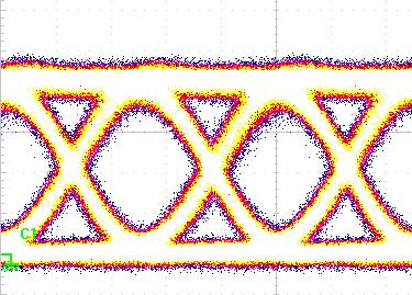
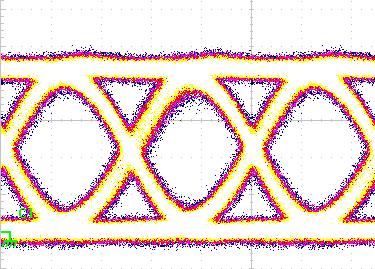
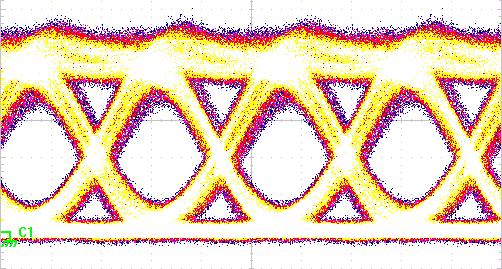
18 Measured Optical Switching Times of a CMOS Driven 2 2 MZI switch ON/OFF ON/OFF normalized power IN OFF T T 2 T, T 22 IN 2 ON ON OFF time (ns) T 2, T 2 time (ns) t /9 = 3.9 ns t /9 =.4 ns B. G. Lee, et al. (CLEO 2) T 2 T 22 8
19 4 4 Switch and CMOS Driver Block Diagram W IN N OUT N IN E OUT CMOS chip Serial Interface 33 µm 52 µm W OUT S IN S OUT E IN E IN S IN MZI 3 MZI 6 model W OUT N OUT Photonic chip W IN N IN MZI 2 MZI MZI 5 MZI 4 function E OUT S OUT 9
20 4 4 Switch Configuration States Of the 2 6 =64 possible states of the 2 2 switches, only 9 are unique. The equivalent states of the 4 4 switch differ by static power dissipation (number of 2 2 switches ON ) In all 9 configuration states, worst case crosstalk between channels is less than - db, insertion loss ~6 db, off chip coupling loss ~ db. State MZI MZI2 MZI3 MZI4 MZI5 MZI6 Power E IN S IN W IN N IN MZI3 MZI2 MZI Area: 3 6 µm 2 (relaxed layout) MZI6 MZI5 MZI4 W OUT N OUT E OUT S OUT 2

21 from serial interface Digital 9-nm CMOS Driver 33 µm 52 µm 2 6 R CONTACT C(Q) I(τ) p-i-n diode model CMOS chip 2 6 Photonic chip Electrical performance of the CMOS driver V DD =.2 V 5 ps ON/OFF optical function Electrical model of the p-i-n diode includes contact resistance, non-linear charge-dependent capacitance and carrier lifetimedependent current source Designed to drive a wide range of capacitive loads and steady state currents with ample speed for switch applications 2

22 4 4 Switch and CMOS Driver Die Photos Serial Interface Drivers with predrivers 5 µm East South West North West North East South 22
 plus forming gas ~25-3 g/bond")
23 Hybrid Packaging of CMOS and Photonics IC probe pads on bottom (not visible) CMOS IC optical coupling Solder Transfer 75 µm pads, 5 µm pitch ~5 µm tall Photonic chip ~3 µm tall Ni-Au Pad Metallization: Photonic chip pads CMOS chip pads solder reflowed again to collapse columns into balls Flux-Free Solder Process: eutectic SnPb solder (26-3 C) plus forming gas ~25-3 g/bond obtained 23

 South Output West Output North Output East")

24 Infrared Images of Static Optical Switching East Input East Input East Input All 6 MZI s OFF West Output MZI 6 ON (.2V) North Output MZI 2 ON (.5V) South Output West Output North Output East Output South Output West Output North Output East Output South Output West Output North Output East Output South Output 24


25 53 nm Measured routing of 4 Gb/s data 4 Gb/s modulator 4 4 Photonic Switch EDFA λ att RX North Input South Input East Input West Input North Output No U-Turn South Output No U-Turn East Output No U-Turn West Output No U-Turn 25


26 Measured routing of 3 4 Gb/s WDM data 53 nm 537 nm 4 Gb/s modulator 4 4 Photonic Switch EDFA EDFA λ att RX 543 nm 53 nm 537 nm 543 nm East Input North Output South Output West Output 26
27 Measured Power Sensitivity Curves All wavelength channels, all output configurations of the 3 4 Gb/s signal tested, showing ~.5 db spread at -2 BER 27
28 Conclusion Full set of CMOS compatible photonic devices: waveguides, splitters, couplers, crossings, WDM structures, etc. waveguide coupled integrated Ge photodetectors MZI and ring based switches, modulators High-density, low-loss edge fiber coupling demonstrated 8 parallel fibers coupled to on-chip waveguides on 2 µm pitch Monolithically integrated technology announced in December 2 Recent CMOS driven hybrid-integrated results include a 5 Gb/s receiver and a ring modulator based 8 Gb/s transmitter Hybrid-integrated packaging process developed Hybrid-integrated CMOS driven 4 4 switch fully tested The authors gratefully acknowledge support from DARPA under contract HR-8-C-2. 28
A 24-Channel 300 Gb/s 8.2 pj/bit Full-Duplex Fiber-Coupled Optical Transceiver Module Based on a Single Holey CMOS IC
 A 24-Channel 300 Gb/s 8.2 pj/bit Full-Duplex Fiber-Coupled Optical Transceiver Module Based on a Single Holey CMOS IC A. Rylyakov, C. Schow, F. Doany, B. Lee, C. Jahnes, Y. Kwark, C.Baks, D. Kuchta, J.
IBM T. J. Watson Research Center IBM Corporation
 Broadband Silicon Photonic Switch Integrated with CMOS Drive Electronics B. G. Lee, J. Van Campenhout, A. V. Rylyakov, C. L. Schow, W. M. J. Green, S. Assefa, M. Yang, F. E. Doany, C. V. Jahnes, R. A.
Lecture: Integration of silicon photonics with electronics. Prepared by Jean-Marc FEDELI CEA-LETI
 Lecture: Integration of silicon photonics with electronics Prepared by Jean-Marc FEDELI CEA-LETI Context The goal is to give optical functionalities to electronics integrated circuit (EIC) The objectives
A Fully Integrated 20 Gb/s Optoelectronic Transceiver Implemented in a Standard
 A Fully Integrated 20 Gb/s Optoelectronic Transceiver Implemented in a Standard 0.13 µm CMOS SOI Technology School of Electrical and Electronic Engineering Yonsei University 이슬아 1. Introduction 2. Architecture
NEXT GENERATION SILICON PHOTONICS FOR COMPUTING AND COMMUNICATION PHILIPPE ABSIL
 NEXT GENERATION SILICON PHOTONICS FOR COMPUTING AND COMMUNICATION PHILIPPE ABSIL OUTLINE Introduction Platform Overview Device Library Overview What s Next? Conclusion OUTLINE Introduction Platform Overview
Electronic-Photonic ICs for Low Cost and Scalable Datacenter Solutions
 Electronic-Photonic ICs for Low Cost and Scalable Datacenter Solutions Christoph Theiss, Director Packaging Christoph.Theiss@sicoya.com 1 SEMICON Europe 2016, October 27 2016 Sicoya Overview Spin-off from
Silicon Photonics Technology Platform To Advance The Development Of Optical Interconnects
 Silicon Photonics Technology Platform To Advance The Development Of Optical Interconnects By Mieke Van Bavel, science editor, imec, Belgium; Joris Van Campenhout, imec, Belgium; Wim Bogaerts, imec s associated
Silicon Photonics: an Industrial Perspective
 Silicon Photonics: an Industrial Perspective Antonio Fincato Advanced Programs R&D, Cornaredo, Italy OUTLINE 2 Introduction Silicon Photonics Concept 300mm (12 ) Photonic Process Main Silicon Photonics
An Example Design using the Analog Photonics Component Library. 3/21/2017 Benjamin Moss
 An Example Design using the Analog Photonics Component Library 3/21/2017 Benjamin Moss Component Library Elements Passive Library Elements: Component Current specs 1 Edge Couplers (Si)
EE 232 Lightwave Devices Optical Interconnects
 EE 232 Lightwave Devices Optical Interconnects Sajjad Moazeni Department of Electrical Engineering & Computer Sciences University of California, Berkeley 1 Emergence of Optical Links US IT Map Hyper-Scale
160-Gb/s Bidirectional Parallel Optical Transceiver Module for Board-Level Interconnects
 160-Gb/s Bidirectional Parallel Optical Transceiver Module for Board-Level Interconnects Fuad Doany, Clint Schow, Jeff Kash C. Baks, D. Kuchta, L. Schares, & R. John IBM T. J. Watson Research Center doany@us.ibm.com
SiGe BiCMOS and Photonic technologies for high frequency and communication applications Andreas Mai
 SiGe BiCMOS and Photonic technologies for high frequency and communication applications Andreas Mai Department Head Technology Outline Introduction & Motivation SiGe HBT device developments for high RF
Convergence Challenges of Photonics with Electronics
 Convergence Challenges of Photonics with Electronics Edward Palen, Ph.D., P.E. PalenSolutions - Optoelectronic Packaging Consulting www.palensolutions.com palensolutions@earthlink.net 415-850-8166 October
Index. Cambridge University Press Silicon Photonics Design Lukas Chrostowski and Michael Hochberg. Index.
 absorption, 69 active tuning, 234 alignment, 394 396 apodization, 164 applications, 7 automated optical probe station, 389 397 avalanche detector, 268 back reflection, 164 band structures, 30 bandwidth
Comparison of Bandwidth Limits for On-card Electrical and Optical Interconnects for 100 Gb/s and Beyond
 Invited Paper Comparison of Bandwidth Limits for On-card Electrical and Optical Interconnects for 1 Gb/s and Beyond Petar Pepeljugoski *, Mark Ritter, Jeffrey A. Kash, Fuad Doany, Clint Schow, Young Kwark,
Silicon Photonics Photo-Detector Announcement. Mario Paniccia Intel Fellow Director, Photonics Technology Lab
 Silicon Photonics Photo-Detector Announcement Mario Paniccia Intel Fellow Director, Photonics Technology Lab Agenda Intel s Silicon Photonics Research 40G Modulator Recap 40G Photodetector Announcement
Low Thermal Resistance Flip-Chip Bonding of 850nm 2-D VCSEL Arrays Capable of 10 Gbit/s/ch Operation
 Low Thermal Resistance Flip-Chip Bonding of 85nm -D VCSEL Arrays Capable of 1 Gbit/s/ch Operation Hendrik Roscher In 3, our well established technology of flip-chip mounted -D 85 nm backside-emitting VCSEL
OPTICAL I/O RESEARCH PROGRAM AT IMEC
 OPTICAL I/O RESEARCH PROGRAM AT IMEC IMEC CORE CMOS PHILIPPE ABSIL, PROGRAM DIRECTOR JORIS VAN CAMPENHOUT, PROGRAM MANAGER SCALING TRENDS IN CHIP-LEVEL I/O RECENT EXAMPLES OF HIGH-BANDWIDTH I/O Graphics
ISSCC 2006 / SESSION 13 / OPTICAL COMMUNICATION / 13.7
 13.7 A 10Gb/s Photonic Modulator and WDM MUX/DEMUX Integrated with Electronics in 0.13µm SOI CMOS Andrew Huang, Cary Gunn, Guo-Liang Li, Yi Liang, Sina Mirsaidi, Adithyaram Narasimha, Thierry Pinguet Luxtera,
Silicon Photonics in Optical Communications. Lars Zimmermann, IHP, Frankfurt (Oder), Germany
, Germany") Silicon Photonics in Optical Communications Lars Zimmermann, IHP, Frankfurt (Oder), Germany Outline IHP who we are Silicon photonics Photonic-electronic integration IHP photonic technology Conclusions
Silicon Photonics in Optical Communications Lars Zimmermann, IHP, Frankfurt (Oder), Germany Outline IHP who we are Silicon photonics Photonic-electronic integration IHP photonic technology Conclusions
Silicon photonics on 3 and 12 μm thick SOI for optical interconnects Timo Aalto VTT Technical Research Centre of Finland
 Silicon photonics on 3 and 12 μm thick SOI for optical interconnects Timo Aalto VTT Technical Research Centre of Finland 5th International Symposium for Optical Interconnect in Data Centres in ECOC, Gothenburg,
Silicon Photonics: A Platform for Integration, Wafer Level Assembly and Packaging
 Silicon Photonics: A Platform for Integration, Wafer Level Assembly and Packaging M. Asghari Kotura Inc April 27 Contents: Who is Kotura Choice of waveguide technology Challenges and merits of Si photonics
ECEN689: Special Topics in Optical Interconnects Circuits and Systems Spring 2016
 ECEN689: Special Topics in Optical Interconnects Circuits and Systems Spring 2016 Lecture 1: Introduction Sam Palermo Analog & Mixed-Signal Center Texas A&M University Class Topics System and design issues
High speed silicon-based optoelectronic devices Delphine Marris-Morini Institut d Electronique Fondamentale, Université Paris Sud
 High speed silicon-based optoelectronic devices Delphine Marris-Morini Institut d Electronique Fondamentale, Université Paris Sud Data centers Optical telecommunications Environment Interconnects Silicon
TDM Photonic Network using Deposited Materials
 TDM Photonic Network using Deposited Materials ROBERT HENDRY, GILBERT HENDRY, KEREN BERGMAN LIGHTWAVE RESEARCH LAB COLUMBIA UNIVERSITY HPEC 2011 Motivation for Silicon Photonics Performance scaling becoming
New advances in silicon photonics Delphine Marris-Morini
 New advances in silicon photonics Delphine Marris-Morini P. Brindel Alcatel-Lucent Bell Lab, Nozay, France New Advances in silicon photonics D. Marris-Morini, L. Virot*, D. Perez-Galacho, X. Le Roux, D.
Si CMOS Technical Working Group
 Si CMOS Technical Working Group CTR, Spring 2008 meeting Markets Interconnects TWG Breakouts Reception TWG reports Si CMOS: photonic integration E-P synergy - Integration - Standardization - Cross-market
APSUNY PDK: Overview and Future Trends
 APSUNY PDK: Overview and Future Trends Erman Timurdogan Analog Photonics, 1 Marina Park Drive, Suite 205, Boston, MA, 02210 erman@analogphotonics.com Silicon Photonics Integrated Circuit Process Design
64 Channel Flip-Chip Mounted Selectively Oxidized GaAs VCSEL Array
 64 Channel Flip-Chip Mounted Selectively Oxidized GaAs VCSEL Array 69 64 Channel Flip-Chip Mounted Selectively Oxidized GaAs VCSEL Array Roland Jäger and Christian Jung We have designed and fabricated
New silicon photonics technology delivers faster data traffic in data centers
 Edition May 2017 Silicon Photonics, Photonics New silicon photonics technology delivers faster data traffic in data centers New transceiver with 10x higher bandwidth than current transceivers. Today, the
Light source approach for silicon photonics transceivers September Fiber to the Chip
 Light source approach for silicon photonics transceivers September 2014 Fiber to the Chip Silicon Photonics Silicon Photonics Technology: Silicon material system & processing techniques to manufacture
Chip Scale Package Fiber Optic Transceiver Integration for Harsh Environments
 Chip Scale Package Fiber Optic Transceiver Integration for Harsh Environments Chuck Tabbert and Charlie Kuznia Ultra Communications, Inc. 990 Park Center Drive, Suite H Vista, CA, USA, 92081 ctabbert@
Heinrich-Hertz-Institut Berlin
 NOVEMBER 24-26, ECOLE POLYTECHNIQUE, PALAISEAU OPTICAL COUPLING OF SOI WAVEGUIDES AND III-V PHOTODETECTORS Ludwig Moerl Heinrich-Hertz-Institut Berlin Photonic Components Dept. Institute for Telecommunications,,
Si Photonics Technology Platform for High Speed Optical Interconnect. Peter De Dobbelaere 9/17/2012
 Si Photonics Technology Platform for High Speed Optical Interconnect Peter De Dobbelaere 9/17/2012 ECOC 2012 - Luxtera Proprietary www.luxtera.com Overview Luxtera: Introduction Silicon Photonics: Introduction
The Past, Present, and Future of Silicon Photonics
 The Past, Present, and Future of Silicon Photonics Myung-Jae Lee High-Speed Circuits & Systems Lab. Dept. of Electrical and Electronic Engineering Yonsei University Outline Introduction A glance at history
Performance of silicon micro ring modulator with an interleaved p-n junction for optical interconnects
 Indian Journal of Pure & Applied Physics Vol. 55, May 2017, pp. 363-367 Performance of silicon micro ring modulator with an interleaved p-n junction for optical interconnects Priyanka Goyal* & Gurjit Kaur
Silicon Photonics Opportunity, applications & Recent Results
 Silicon Photonics Opportunity, applications & Recent Results Dr. Mario Paniccia Intel Fellow Director, Photonics Technology Lab Intel Corporation www.intel.com/go/sp Purdue University Oct 5 2007 Agenda
The Light at the End of the Wire. Dana Vantrease + HP Labs + Mikko Lipasti
 The Light at the End of the Wire Dana Vantrease + HP Labs + Mikko Lipasti 1 Goals of This Talk Why should we (architects) be interested in optics? How does on-chip optics work? What can we build with optics?
A tunable Si CMOS photonic multiplexer/de-multiplexer
 A tunable Si CMOS photonic multiplexer/de-multiplexer OPTICS EXPRESS Published : 25 Feb 2010 MinJae Jung M.I.C.S Content 1. Introduction 2. CMOS photonic 1x4 Si ring multiplexer Principle of add/drop filter
Near/Mid-Infrared Heterogeneous Si Photonics
 PHOTONICS RESEARCH GROUP Near/Mid-Infrared Heterogeneous Si Photonics Zhechao Wang, PhD Photonics Research Group Ghent University / imec, Belgium ICSI-9, Montreal PHOTONICS RESEARCH GROUP 1 Outline Ge-on-Si
Optical Integrated Devices in Silicon On Insulator for VLSI Photonics
 Optical Integrated Devices in Silicon On Insulator for VLSI Photonics Design, Modelling, Fabrication & Characterization Piero Orlandi 1 Possible Approaches Reduced Design time Transparent Technology Shared
Examination Optoelectronic Communication Technology. April 11, Name: Student ID number: OCT1 1: OCT 2: OCT 3: OCT 4: Total: Grade:
 Examination Optoelectronic Communication Technology April, 26 Name: Student ID number: OCT : OCT 2: OCT 3: OCT 4: Total: Grade: Declaration of Consent I hereby agree to have my exam results published on
Chapter 10 WDM concepts and components
 Chapter 10 WDM concepts and components - Outline 10.1 Operational principle of WDM 10. Passive Components - The x Fiber Coupler - Scattering Matrix Representation - The x Waveguide Coupler - Mach-Zehnder
Silicon photonics with low loss and small polarization dependency. Timo Aalto VTT Technical Research Centre of Finland
 Silicon photonics with low loss and small polarization dependency Timo Aalto VTT Technical Research Centre of Finland EPIC workshop in Tokyo, 9 th November 2017 VTT Technical Research Center of Finland
Foundry processes for silicon photonics. Pieter Dumon 7 April 2010 ECIO
 Foundry processes for silicon photonics Pieter Dumon 7 April 2010 ECIO Photonics Research Group http://photonics.intec.ugent.be epixfab Prototyping Training Multi project wafer access to silicon photonic
Silicon Carrier-Depletion-Based Mach-Zehnder and Ring Modulators with Different Doping Patterns for Telecommunication and Optical Interconnect
 Silicon Carrier-Depletion-Based Mach-Zehnder and Ring Modulators with Different Doping Patterns for Telecommunication and Optical Interconnect Hui Yu, Marianna Pantouvaki*, Joris Van Campenhout*, Katarzyna
Silicon Optical Modulator
 Silicon Optical Modulator Silicon Optical Photonics Nature Photonics Published online: 30 July 2010 Byung-Min Yu 24 April 2014 High-Speed Circuits & Systems Lab. Dept. of Electrical and Electronic Engineering
Optical technologies for data communication in large parallel systems
 Journal of Instrumentation OPEN ACCESS Optical technologies for data communication in large parallel systems To cite this article: M B Ritter et al View the article online for updates and enhancements.
Scalable Electro-optical Assembly Techniques for Silicon Photonics
 Scalable Electro-optical Assembly Techniques for Silicon Photonics Bert Jan Offrein, Tymon Barwicz, Paul Fortier OIDA Workshop on Manufacturing Trends for Integrated Photonics Outline Broadband large channel
Opportunities and challenges of silicon photonics based System-In-Package
 Opportunities and challenges of silicon photonics based System-In-Package ECTC 2014 Panel session : Emerging Technologies and Market Trends of Silicon Photonics Speaker : Stéphane Bernabé (Leti Photonics
MODELING AND EVALUATION OF CHIP-TO-CHIP SCALE SILICON PHOTONIC NETWORKS
 1 MODELING AND EVALUATION OF CHIP-TO-CHIP SCALE SILICON PHOTONIC NETWORKS Robert Hendry, Dessislava Nikolova, Sébastien Rumley, Keren Bergman Columbia University HOTI 2014 2 Chip-to-chip optical networks
Flip chip Assembly with Sub-micron 3D Re-alignment via Solder Surface Tension
 Flip chip Assembly with Sub-micron 3D Re-alignment via Solder Surface Tension Jae-Woong Nah*, Yves Martin, Swetha Kamlapurkar, Sebastian Engelmann, Robert L. Bruce, and Tymon Barwicz IBM T. J. Watson Research
CHAPTER 2 POLARIZATION SPLITTER- ROTATOR BASED ON A DOUBLE- ETCHED DIRECTIONAL COUPLER
 CHAPTER 2 POLARIZATION SPLITTER- ROTATOR BASED ON A DOUBLE- ETCHED DIRECTIONAL COUPLER As we discussed in chapter 1, silicon photonics has received much attention in the last decade. The main reason is
Nanophotonics for low latency optical integrated circuits
 Nanophotonics for low latency optical integrated circuits Akihiko Shinya NTT Basic Research Labs., Nanophotonics Center, NTT Corporation MPSoC 17, Annecy, France Outline Low latency optical circuit BDD
for optical communication system
 High speed Ge waveguide detector for optical communication system Xingjun Wang, Zhijuan Tu and Zhiping Zhou State Key Laboratory of Advanced Optical Communication Systems and Networks, School of Electronics
OTemp: Optical Thermal Effect Modeling Platform User Manual
 OTemp: Optical Thermal Effect Modeling Platform User Manual Version 1., July 214 Mobile Computing System Lab Department of Electronic and Computer Engineering The Hong Kong University of Science and Technology
Integration of Optoelectronic and RF Devices for Applications in Optical Interconnect and Wireless Communication
 Integration of Optoelectronic and RF Devices for Applications in Optical Interconnect and Wireless Communication Zhaoran (Rena) Huang Assistant Professor Department of Electrical, Computer and System Engineering
Low-Power, 10-Gbps 1.5-Vpp Differential CMOS Driver for a Silicon Electro-Optic Ring Modulator
 Low-Power, 10-Gbps 1.5-Vpp Differential CMOS Driver for a Silicon Electro-Optic Ring Modulator Michal Rakowski 1,2, Julien Ryckaert 1, Marianna Pantouvaki 1, Hui Yu 3, Wim Bogaerts 3, Kristin de Meyer
Hybrid Integration Technology of Silicon Optical Waveguide and Electronic Circuit
 Hybrid Integration Technology of Silicon Optical Waveguide and Electronic Circuit Daisuke Shimura Kyoko Kotani Hiroyuki Takahashi Hideaki Okayama Hiroki Yaegashi Due to the proliferation of broadband services
EPIC: The Convergence of Electronics & Photonics
 EPIC: The Convergence of Electronics & Photonics K-Y Tu, Y.K. Chen, D.M. Gill, M. Rasras, S.S. Patel, A.E. White ell Laboratories, Lucent Technologies M. Grove, D.C. Carothers, A.T. Pomerene, T. Conway
Petar Pepeljugoski IBM T.J. Watson Research Center
 Comparison of Bandwidth Limits for On-Card Electrical and Optical Interconnects for 100 Gb/s and Beyond Petar Pepeljugoski IBM T.J. Watson Research Center Collaborators and Acknowledgements Fuad Doany,
VERSATILE SILICON PHOTONIC PLATFORM FOR DATACOM AND COMPUTERCOM APPLICATIONS. B Szelag CEA-Leti
 VERSATILE SILICON PHOTONIC PLATFORM FOR DATACOM AND COMPUTERCOM APPLICATIONS B Szelag CEA-Leti OUTLINE Silicon photonic : 200mm CMOS core technology towards 300mm Emergent needs vs core process Technological
Low-power 2.5 Gbps VCSEL driver in 0.5 µm CMOS technology
 Low-power 2.5 Gbps VCSEL driver in 0.5 µm CMOS technology Bindu Madhavan and A. F. J. Levi Department of Electrical Engineering University of Southern California Los Angeles, California 90089-1111 Indexing
Si and InP Integration in the HELIOS project
 Si and InP Integration in the HELIOS project J.M. Fedeli CEA-LETI, Grenoble ( France) ECOC 2009 1 Basic information about HELIOS HELIOS photonics ELectronics functional Integration on CMOS www.helios-project.eu
UNIT - 7 WDM CONCEPTS AND COMPONENTS
 UNIT - 7 WDM CONCEPTS AND COMPONENTS WDM concepts, overview of WDM operation principles, WDM standards, Mach-Zehender interferometer, multiplexer, Isolators and circulators, direct thin film filters, active
JOURNAL OF LIGHTWAVE TECHNOLOGY, VOL. 27, NO. 7, APRIL 1,
 JOURNAL OF LIGHTWAVE TECHNOLOGY, VOL. 27, NO. 7, APRIL 1, 2009 915 A Single-Chip CMOS-Based Parallel Optical Transceiver Capable of 240-Gb/s Bidirectional Data Rates Clint L. Schow, Fuad E. Doany, Member,
Integrated photonic circuit in silicon on insulator for Fourier domain optical coherence tomography
 Integrated photonic circuit in silicon on insulator for Fourier domain optical coherence tomography Günay Yurtsever *,a, Pieter Dumon a, Wim Bogaerts a, Roel Baets a a Ghent University IMEC, Photonics
The Development of the 1060 nm 28 Gb/s VCSEL and the Characteristics of the Multi-mode Fiber Link
 Special Issue Optical Communication The Development of the 16 nm 28 Gb/s VCSEL and the Characteristics of the Multi-mode Fiber Link Tomofumi Kise* 1, Toshihito Suzuki* 2, Masaki Funabashi* 1, Kazuya Nagashima*
Microphotonics Readiness for Commercial CMOS Manufacturing. Marco Romagnoli
 Microphotonics Readiness for Commercial CMOS Manufacturing Marco Romagnoli MicroPhotonics Consortium meeting MIT, Cambridge October 15 th, 2012 Passive optical structures based on SOI technology Building
Signal Integrity Modeling and Measurement of TSV in 3D IC
 Signal Integrity Modeling and Measurement of TSV in 3D IC Joungho Kim KAIST joungho@ee.kaist.ac.kr 1 Contents 1) Introduction 2) 2.5D/3D Architectures with TSV and Interposer 3) Signal integrity, Channel
Overview of short-reach optical interconnects: from VCSELs to silicon nanophotonics
 Acknowledgements: J. Cunningham, R. Ho, X. Zheng, J. Lexau, H. Thacker, J. Yao, Y. Luo, G. Li, I. Shubin, F. Liu, D. Patil, K. Raj, and J. Mitchell M. Asghari T. Pinguet Overview
CHAPTER 4 RESULTS. 4.1 Introduction
 CHAPTER 4 RESULTS 4.1 Introduction In this chapter focus are given more on WDM system. The results which are obtained mainly from the simulation work are presented. In simulation analysis, the study will
Silicon-On-Insulator based guided wave optical clock distribution
 Silicon-On-Insulator based guided wave optical clock distribution K. E. Moselund, P. Dainesi, and A. M. Ionescu Electronics Laboratory Swiss Federal Institute of Technology People and funding EPFL Project
Silicon Photonics Transceivers for Hyper Scale Datacenters: Deployment and Roadmap
 Silicon Photonics Transceivers for Hyper Scale Datacenters: Deployment and Roadmap Peter De Dobbelaere Luxtera Inc. 09/19/2016 Luxtera Proprietary www.luxtera.com Luxtera Company Introduction $100B+ Shift
Innovations in Photonic Integration Platforms
 Innovations in Photonic Integration Platforms September 20, 20 Burgeoning Growth Demand Disruptive Technology Video content is fast becoming a larger percentage of total internet traffic 50% Video services
IEEE JOURNAL OF SELECTED TOPICS IN QUANTUM ELECTRONICS 2010 Silicon Photonic Circuits: On-CMOS Integration, Fiber Optical Coupling, and Packaging
 IEEE JOURNAL OF SELECTED TOPICS IN QUANTUM ELECTRONICS 2010 Silicon Photonic Circuits: On-CMOS Integration, Fiber Optical Coupling, and Packaging Christophe Kopp, St ephane Bernab e, Badhise Ben Bakir,
Photonic Integrated Circuits Made in Berlin
 Fraunhofer Heinrich Hertz Institute Photonic Integrated Circuits Made in Berlin Photonic integration Workshop, Columbia University, NYC October 2015 Moritz Baier, Francisco M. Soares, Norbert Grote Fraunhofer
Addressing Link-Level Design Tradeoffs for Integrated Photonic Interconnects
 Addressing Link-Level Design Tradeoffs for Integrated Photonic Interconnects Michael Georgas, Jonathan Leu, Benjamin Moss, Chen Sun and Vladimir Stojanović Massachusetts Institute of Technology CICC 2011
Compact two-mode (de)multiplexer based on symmetric Y-junction and Multimode interference waveguides
multiplexer based on symmetric Y-junction and Multimode interference waveguides") Compact two-mode (de)multiplexer based on symmetric Y-junction and Multimode interference waveguides Yaming Li, Chong Li, Chuanbo Li, Buwen Cheng, * and Chunlai Xue State Key Laboratory on Integrated Optoelectronics,
Compact two-mode (de)multiplexer based on symmetric Y-junction and Multimode interference waveguides Yaming Li, Chong Li, Chuanbo Li, Buwen Cheng, * and Chunlai Xue State Key Laboratory on Integrated Optoelectronics,
High-speed Ge photodetector monolithically integrated with large cross silicon-on-insulator waveguide
 [ APPLIED PHYSICS LETTERS ] High-speed Ge photodetector monolithically integrated with large cross silicon-on-insulator waveguide Dazeng Feng, Shirong Liao, Roshanak Shafiiha. etc Contents 1. Introduction
Monolithic Integra/on of O-band Photonic Transceivers in a Zero-change 32nm SOI CMOS
 Monolithic Integra/on of O-band Photonic Transceivers in a Zero-change 32nm SOI CMOS S. Moazeni 1, A. Atabaki 2, D. Cheian 2, S. Lin 1, R. J. Ram 2, and V. Stojanović 1 1 Department of EECS, University
Flip-Chip for MM-Wave and Broadband Packaging
 1 Flip-Chip for MM-Wave and Broadband Packaging Wolfgang Heinrich Ferdinand-Braun-Institut für Höchstfrequenztechnik (FBH) Berlin / Germany with contributions by F. J. Schmückle Motivation Growing markets
ECEN620: Network Theory Broadband Circuit Design Fall 2014
 ECEN620: Network Theory Broadband Circuit Design Fall 2014 Lecture 19: High-Speed Transmitters Sam Palermo Analog & Mixed-Signal Center Texas A&M University Announcements Exam 3 is on Friday Dec 5 Focus
Silicon Integrated Photonics
 Silicon Integrated Photonics Dr. Mario Paniccia, Director Photonics Technology Lab Intel Corporation IEEE CAS Society May 16, 2005 For More Info http://www.intel.com/technology/silicon/sp/ Intel Corporation
A CMOS-compatible silicon photonic platform for high-speed integrated opto-electronics
 Invited Paper A CMOS-compatible silicon photonic platform for high-speed integrated opto-electronics Christophe Galland 1, Ari Novack 3,4, Yang Liu 1, Ran Ding 1, Michael Gould 2, Tom Baehr-Jones 1, Qi
SYLLABUS Optical Fiber Communication
 SYLLABUS Optical Fiber Communication Subject Code : IA Marks : 25 No. of Lecture Hrs/Week : 04 Exam Hours : 03 Total no. of Lecture Hrs. : 52 Exam Marks : 100 UNIT - 1 PART - A OVERVIEW OF OPTICAL FIBER
Wafer-scale 3D integration of silicon-on-insulator RF amplifiers
 Wafer-scale integration of silicon-on-insulator RF amplifiers The MIT Faculty has made this article openly available. Please share how this access benefits you. Your story matters. Citation As Published
3D IC-Package-Board Co-analysis using 3D EM Simulation for Mobile Applications
 3D IC-Package-Board Co-analysis using 3D EM Simulation for Mobile Applications Darryl Kostka, CST of America Taigon Song and Sung Kyu Lim, Georgia Institute of Technology Outline Introduction TSV Array
- no emitters/amplifiers available. - complex process - no CMOS-compatible
 Advantages of photonic integrated circuits (PICs) in Microwave Photonics (MWP): compactness low-power consumption, stability flexibility possibility of aggregating optics and electronics functionalities
Directional coupler (2 Students)
") Directional coupler (2 Students) The goal of this project is to make a 2 by 2 optical directional coupler with a defined power ratio for the two output branches. The directional coupler should be optimized
Directional coupler (2 Students) The goal of this project is to make a 2 by 2 optical directional coupler with a defined power ratio for the two output branches. The directional coupler should be optimized
Mitigation of Mode Partition Noise in Quantum-dash Fabry-Perot Mode-locked Lasers using Manchester Encoding
 Mitigation of Mode Partition Noise in Quantum-dash Fabry-Perot Mode-locked Lasers using Manchester Encoding Mohamed Chaibi*, Laurent Bramerie, Sébastien Lobo, Christophe Peucheret *chaibi@enssat.fr FOTON
Zukunftstechnologie Dünnglasbasierte elektrooptische. Research Center of Microperipheric Technologies
 Zukunftstechnologie Dünnglasbasierte elektrooptische Baugruppenträger Dr. Henning Schröder Fraunhofer IZM, Berlin, Germany Today/Overview Motivation: external roadmaps High Bandwidth and Channel Density
Lecture 4 INTEGRATED PHOTONICS
 Lecture 4 INTEGRATED PHOTONICS What is photonics? Photonic applications use the photon in the same way that electronic applications use the electron. Devices that run on light have a number of advantages
ECEN689: Special Topics in Optical Interconnects Circuits and Systems Spring 2016
 ECEN689: Special Topics in Optical Interconnects Circuits and Systems Spring 2016 Lecture 9: Mach-Zehnder Modulator Transmitters Sam Palermo Analog & Mixed-Signal Center Texas A&M University Mach-Zehnder
MICRO RING MODULATOR. Dae-hyun Kwon. High-speed circuits and Systems Laboratory
 MICRO RING MODULATOR Dae-hyun Kwon High-speed circuits and Systems Laboratory Paper preview Title of the paper Low Vpp, ultralow-energy, compact, high-speed silicon electro-optic modulator Publication
Silicon photonics integration roadmap for applications in computing systems
 Silicon photonics integration roadmap for applications in computing systems Bert Jan Offrein Neuromorphic Devices and Systems Group 2016 IBM Corporation Outline Photonics and computing? The interconnect
Envisioning the Future of Optoelectronic Interconnects:
 Envisioning the Future of Optoelectronic Interconnects: The Production Economics of InP and Si Platforms for 100G Ethernet LAN Transceivers Shan Liu Dr. Erica Fuchs Prof. Randolph Kirchain MIT Microphotonics
Microcircuit Electrical Issues
 Microcircuit Electrical Issues Distortion The frequency at which transmitted power has dropped to 50 percent of the injected power is called the "3 db" point and is used to define the bandwidth of the
PROJECT FINAL REPORT
 PROJECT FINAL REPORT Grant Agreement number: FP7-224312 Project acronym: HELIOS Project title: photonics ELectronics functional Integration on CMOS Funding Scheme: Large Scale Integrating Project Period
Silicon Photonics Opportunity, Applicatoins & Recent Results. Mario Paniccia, Director Photonics Technology Lab Intel Corporation
 Silicon Photonics Opportunity, Applicatoins & Recent Results Mario Paniccia, Director Photonics Technology Lab Intel Corporation Intel Corporation CREOL April 1 2005 Agenda Opportunity for Silicon Photonics