Homework 2 Solutions. Perform.op analysis, the small-signal parameters of M1 and M2 are shown below.
|
|
|
- Preston Cain
- 5 years ago
- Views:
Transcription
1 Problem 1 Homework 2 Solutions 1) Circuit schematic Perform.op analysis, the small-signal parameters of M1 and M2 are shown below. Small-signal parameters of M1 gds = 9.723u gm = 234.5u region = 2 vds = vgs = 1.256
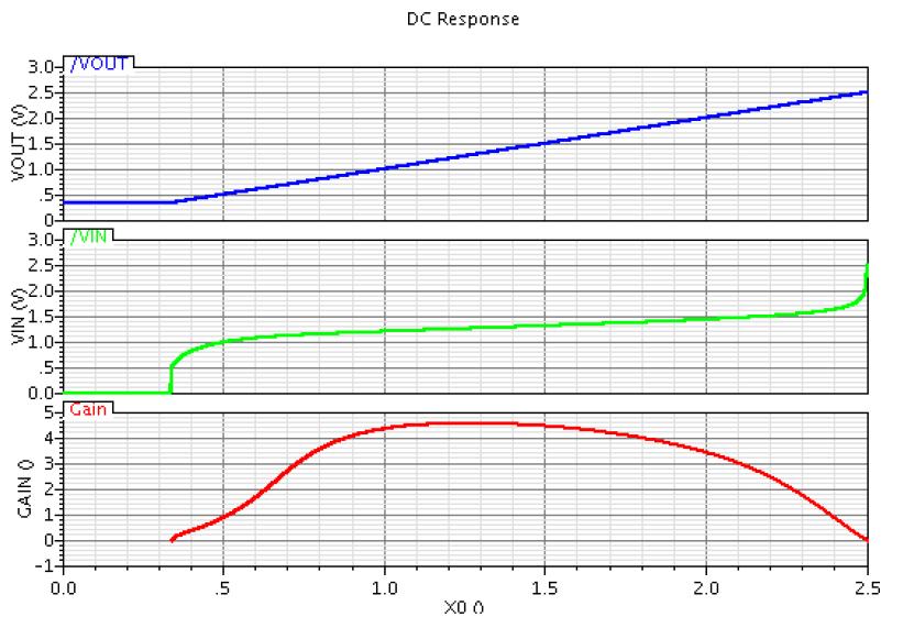
2 vth = 488m Small-signal parameters of M2 gds = 9.723u gm = 234.5u region = 2 vds = vgs = vth = 488m M1 and M2 both are in the saturation region. 2) For M1, Small-signal gain is, A G R G 234.5u VM, 1 m out m out ds1 1 So, small-signal gain of M1 is For M2, Small-signal gain is, A G R G 234.5u VM, 1 m out R 1/ g R 9.11k m out ds1 1 So, small-signal gain of M2 is Total voltage gain is, AV AV, M1 AV, M R 1/ g R 9.11k 3) Plot of voltage gain vs. output voltage
3 In order to plot the voltage gain versus output voltage, we need to create the feedback loop and sweep DC output voltage, the schematic is shown below. With the above schematic, we could sweep DC output voltage. Assume that the differential amplifier is the ideal VCVS with very large gain, and its maximum and minimum output voltage is 2.5V and 0V respectively. Therefore, DC output voltage is equal to the input of amplifier and sweeping it is considered as sweeping output voltage. The input voltage of M1, Vi, should change with sweeping output voltage, so that we could calculate the voltage gain. (In calculator, select derive from the special function, for example, use deriv(vo)/deriv(vi) to calculate the small signal gain). The simulation results are shown below.
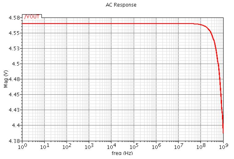
4 4) Plot of small-signal gain vs. frequency
5 Since the AC magnitude of input voltage source is 1, output voltage is directly equal to the voltage gain. Based on the simulation results, the voltage gain is also 4.565, which is almost the same as that of calculation results in problem Output impedance is, R 1/ g R 9.11k o ds Schematic to extract output impedance Ro, Ro = Vx/Ix, if we set AC magnitude Vx=1, then output impedance Ro = 1/Ix. Based on the schematic shown above, the simulation result of Ix is shown below.

6 Ix = uA, therefore, Ro = 1/109.72u = 9.11kΩ, which is the same as the calculated output impedance in problem 5. 7) Large-signal swing plot,
7 The upper limit of large-signal swing is the voltage across the resistor R2, the maximum value for output voltage swing is V DD, when M2 is cut-off. The low limit of large-signal swing is the overdrive voltage of M1. In order to make sure that M1 is in the saturation region, output voltage should be larger than V ov,m1. Problem 2 1) Perform.op analysis, the small-signal parameters of M1 and M2 are shown below. Small-signal parameters of M1 gds = 31.98u
8 gm = 1.561m gmbs = 235.8u region = 2 vds = vgs = 801.1m vth = 721.6m Small-signal parameters of M2 gds = 5.255u gm = 272.3u gmbs = 55.1u region = 2 vds = vgs = 796m vth = 579.8m M1 and M2 are both in the saturation region. 2) For M1, Small-signal gain is, A G R G 1.561m VM, 1 m out out m1 mb1 ds1 1 m R 1/ g 1/ g 1/ g R 0.518k So, small-signal gain of M1 is
9 For M2, Small-signal gain is, A G R G 272.3u VM, 2 m out out m2 mb2 ds2 2 m R 1/ g 1/ g 1/ g R 2.31k So, small-signal gain of M2 is Total voltage gain is, A A, 1 A, V V M V M 3) Plot of voltage gain vs. output voltage 4) Plot of small-signal gain vs. frequency

10 Since the AC magnitude of input voltage source is 1, output voltage is directly equal to the voltage gain. Based on the simulation results, the voltage gain is 0.509, which is the same as that of calculation results in problem 2. 5) Output impedance is, R 1/ g 1/ g 1/ g R 2.31k o m2 mb2 ds2 2 6)
11 Ro=Vx/Ix, if we set AC magnitude as Vx=1, then the output impedance Ro=1/Ix. Based on the schematic shown above, the simulation result of Ix is shown below.

12 Ix=432.53u, therefore, Ro=1/432.53u=2.31kΩ, which is the same as the calculated output impedance in problem 5. 7) Large-signal swing plot

13 The upper limit of large-signal swing is the overdrive voltage of M1 and the Gate-to-Source voltage of M2, the maximum value for output voltage is V DD -V ov,m1 -V GS,M2. (Note that, if we assume that the maximum input voltage is V DD, the maximum output voltage should be V DD -V GS,M1 -V GS,M2.) The low limit of large-signal swing is very close to the ground, when M2 is cut-off. Connect the bulk to the source for both two transistors, and repeat above 1)
14 (Note, the size of M1 and M2 are changed, however, if the size is not changed in the homework, the answer is still acceptable as long as the simulation is rational.) 1) Perform.op analysis, the results are shown as the following part. Small-signal parameters of M1 gds = 13.48u gm = 597.4u region = 2 vds = vgs = 799.2m vth = 489.6m Small-signal parameters of M2 gds = 3.986u
15 gm = 198.1u region = 2 vds = vgs = 794.7m vth = 488.1m 2) For M1, Small-signal gain is, A G R G 597.4u VM, 1 m out R 1/ g 1/ g R 1.41k m out m1 ds1 1 So, small-signal gain of M1 is For M2, Small-signal gain is, A G R G 198.1u VM, 2 m out R 1/ g 1/ g R 3.31k m out m2 ds2 2 So, small-signal gain of M2 is Total voltage gain is, A A, 1 A, V V M V M 3) Plot of voltage gain vs. output voltage

16 4) Plot of small-signal gain vs. frequency Since the AC magnitude of input voltage source is 1, output voltage is directly equal to the voltage gain. Based on the simulation results, the
17 voltage gain is 0.551, which is almost the same as that of calculation results in problem 2. 5) Output impedance is Ro gm 1/ g R 3.31k 6) 1/ 2 ds2 2

18 The analysis part is the same as the last question. Ix=302.02u, therefore, Ro=1/302.02u=3.31kΩ, which is the same as the calculated output impedance in problem 5. 7) Large-signal swing plot
19 The analysis part is the same as the previous part.
8. Characteristics of Field Effect Transistor (MOSFET)
") 1 8. Characteristics of Field Effect Transistor (MOSFET) 8.1. Objectives The purpose of this experiment is to measure input and output characteristics of n-channel and p- channel field effect transistors
1 8. Characteristics of Field Effect Transistor (MOSFET) 8.1. Objectives The purpose of this experiment is to measure input and output characteristics of n-channel and p- channel field effect transistors
EECS3611 Analog Integrated Circuit Design. Lecture 3. Current Source and Current Mirror
 EECS3611 Analog ntegrated Circuit Design Lecture 3 Current Source and Current Mirror ntroduction Before any device can be used in any application, it has to be properly biased so that small signal AC parameters
0.85V. 2. vs. I W / L
 EE501 Lab3 Exploring Transistor Characteristics and Design Common-Source Amplifiers Lab report due on September 22, 2016 Objectives: 1. Be familiar with characteristics of MOSFET such as gain, speed, power,
ECE315 / ECE515 Lecture 7 Date:
 Lecture 7 ate: 01.09.2016 CG Amplifier Examples Biasing in MOS Amplifier Circuits Common Gate (CG) Amplifier CG Amplifier- nput is applied at the Source and the output is sensed at the rain. The Gate terminal
Session 2 MOS Transistor for RF Circuits
 Session 2 MOS Transistor for RF Circuits Session Speaker Chandramohan P. Session Contents MOS transistor basics MOS equivalent circuit Single stage amplifiers Opamp design Session objectives To understand
Nonlinear Macromodeling of Amplifiers and Applications to Filter Design.
 ECEN 622(ESS) Nonlinear Macromodeling of Amplifiers and Applications to Filter Design. By Edgar Sanchez-Sinencio Thanks to Heng Zhang for part of the material OP AMP MACROMODELS Systems containing a significant
UNIVERSITY OF NORTH CAROLINA AT CHARLOTTE Department of Electrical and Computer Engineering
 UNIVERSITY OF NORTH CAROLINA AT CHARLOTTE Department of Electrical and Computer Engineering EXPERIMENT 8 MOSFET AMPLIFIER CONFIGURATIONS AND INPUT/OUTPUT IMPEDANCE OBJECTIVES The purpose of this experiment
ECE315 / ECE515 Lecture 8 Date:
 ECE35 / ECE55 Lecture 8 Date: 05.09.06 CS Amplifier with Constant Current Source Current Steering Circuits CS Stage Followed by CG Stage Cascode as Current Source Cascode as Amplifier ECE35 / ECE55 CS
Lecture 13. Biasing and Loading Single Stage FET Amplifiers. The Building Blocks of Analog Circuits - III
 Lecture 3 Biasing and Loading Single Stage FET Amplifiers The Building Blocks of Analog Circuits III In this lecture you will learn: Current biasing of circuits Current sources and sinks for CS, CG, and
MOSFET Biasing Supplement for Laboratory Experiment 5 EE348L. Spring 2005
 MOSFET Biasing Supplement for Laboratory Experiment 5 EE348L Spring 2005 B. Madhavan Spring 2005 B. Madhavan Page 1 of 10 EE348L, Spring 2005 5 Laboratory Assignment 5 biasing supplement 5.1 Biasing a
CS and CE amplifiers with loads:
 CS and CE amplifiers with loads: The Common-Source Circuit The most basic IC MOS amplifier is shown in fig.(1). The source of MOS transistor is grounded, also the drain resistor RD replaced by a constant-current
Nonlinear Macromodeling of Amplifiers and Applications to Filter Design.
 ECEN 622 Nonlinear Macromodeling of Amplifiers and Applications to Filter Design. By Edgar Sanchez-Sinencio Thanks to Heng Zhang for part of the material OP AMP MACROMODELS Systems containing a significant
6.002 Circuits and Electronics Final Exam Practice Set 1
 MASSACHUSETTS INSTITUTE OF TECHNOLOGY DEPARTMENT OF ELECTRICAL ENGINEERING AND COMPUTER SCIENCE 6.002 Circuits and Electronics Set 1 Problem 1 Figure 1 shows a simplified small-signal model of a certain
Chapter 4 Single-stage MOS amplifiers
 Chapter 4 Single-stage MOS amplifiers ELEC-H402/CH4: Single-stage MOS amplifiers 1 Single-stage MOS amplifiers NMOS as an amplifier: example of common-source circuit NMOS amplifier example Introduction
EE 501 Lab 1 Exploring Transistor Characteristics
 Objectives: Tasks: EE 501 Lab 1 Exploring Transistor Characteristics Lab report due on Sep 8th, 2011 1. Make sure you have your cadence 6 work properly 2. Familiar with characteristics of MOSFET such as
Common Gate Stage Cascode Stage. Claudio Talarico, Gonzaga University
 Common Gate Stage Cascode Stage Claudio Talarico, Gonzaga University Common Gate Stage The overdrive due to V B must be consistent with the current pulled by the DC source I B careful with signs: v gs
Experiment 5 Single-Stage MOS Amplifiers
 Experiment 5 Single-Stage MOS Amplifiers B. Cagdaser, H. Chong, R. Lu, and R. T. Howe UC Berkeley EE 105 Fall 2005 1 Objective This is the first lab dealing with the use of transistors in amplifiers. We
ENGI0531 Lab 2 Tutorial
 ENGI0531 Lab 2 Tutorial Transient Analysis, Operating Points, Parameters and other miscellany Lakehead University Greg Toombs Winter 2009 1. Constructing the Circuit Copying a Cell View Start Cadence as
Solid State Devices & Circuits. 18. Advanced Techniques
 ECE 442 Solid State Devices & Circuits 18. Advanced Techniques Jose E. Schutt-Aine Electrical l&c Computer Engineering i University of Illinois jschutt@emlab.uiuc.edu 1 Darlington Configuration - Popular
Analog Integrated Circuit Configurations
 Analog Integrated Circuit Configurations Basic stages: differential pairs, current biasing, mirrors, etc. Approximate analysis for initial design MOSFET and Bipolar circuits Basic Current Bias Sources
ETIN25 Analogue IC Design. Laboratory Manual Lab 2
 Department of Electrical and Information Technology LTH ETIN25 Analogue IC Design Laboratory Manual Lab 2 Jonas Lindstrand Martin Liliebladh Markus Törmänen September 2011 Laboratory 2: Design and Simulation
Chapter 3: Operational Amplifiers
 Chapter 3: Operational Amplifiers 1 OPERATIONAL AMPLIFIERS Having learned the basic laws and theorems for circuit analysis, we are now ready to study an active circuit element of paramount importance:
ECEN474: (Analog) VLSI Circuit Design Fall 2011
 VLSI Circuit Design Fall 2011") ECEN474: (Analog) VLSI Circuit Design Fall 20 Lecture 22: Output Stages Sebastian Hoyos Analog & Mixed-Signal Center Texas A&M University Agenda Output Stages Source Follower (Class A) Push-Pull (Class
ECEN474: (Analog) VLSI Circuit Design Fall 20 Lecture 22: Output Stages Sebastian Hoyos Analog & Mixed-Signal Center Texas A&M University Agenda Output Stages Source Follower (Class A) Push-Pull (Class
ECEN 474/704 Lab 6: Differential Pairs
 ECEN 474/704 Lab 6: Differential Pairs Objective Design, simulate and layout various differential pairs used in different types of differential amplifiers such as operational transconductance amplifiers
QUESTION BANK for Analog Electronics 4EC111 *
 OpenStax-CNX module: m54983 1 QUESTION BANK for Analog Electronics 4EC111 * Bijay_Kumar Sharma This work is produced by OpenStax-CNX and licensed under the Creative Commons Attribution License 4.0 Abstract
Common-Source Amplifiers
 Lab 2: Common-Source Amplifiers Introduction The common-source stage is the most basic amplifier stage encountered in CMOS analog circuits. Because of its very high input impedance, moderate-to-high gain,
Differential Amplifier Design
 Fall - 2009 EE114 - Design Project Differential Amplifier Design Submitted by Piyush Keshri (0559 4497) Jeffrey Tu (0554 4565) On November 20th, 2009 EE114 - Design Project Stanford University Page No.
D n ox GS THN DS GS THN DS GS THN. D n ox GS THN DS GS THN DS GS THN
 Name: EXAM #3 Closed book, closed notes. Calculators may be used for numeric computations only. All work is to be your own - show your work for maximum partial credit. Data: Use the following data in all
An electronic unit that behaves like a voltagecontrolled
 1 An electronic unit that behaves like a voltagecontrolled voltage source. An active circuit element that amplifies, sums, subtracts, multiply, divide, differentiate or integrates a signal 2 A typical
Differential Amplifiers. EE105 - Spring 2007 Microelectronic Devices and Circuits. Audio Amplifier Example. Small-Signal Model for Bipolar Transistor
 EE105 - Spring 007 Microelectronic Devices and Circuits Lecture 8 Differential Amplifiers Differential Amplifiers General Considerations MOS Differential Pair Cascode Differential Amplifiers Common-Mode
PHYSICS 330 LAB Operational Amplifier Frequency Response
 PHYSICS 330 LAB Operational Amplifier Frequency Response Objectives: To measure and plot the frequency response of an operational amplifier circuit. History: Operational amplifiers are among the most widely
EE311: Electrical Engineering Junior Lab, Fall 2006 Experiment 4: Basic MOSFET Characteristics and Analog Circuits
 EE311: Electrical Engineering Junior Lab, Fall 2006 Experiment 4: Basic MOSFET Characteristics and Analog Circuits Objective This experiment is designed for students to get familiar with the basic properties
Operational Amplifiers
 CHAPTER 9 Operational Amplifiers Analog IC Analysis and Design 9- Chih-Cheng Hsieh Outline. General Consideration. One-Stage Op Amps / Two-Stage Op Amps 3. Gain Boosting 4. Common-Mode Feedback 5. Input
ECE 2274 MOSFET Voltmeter. Richard Cooper
 ECE 2274 MOSFET Voltmeter Richard Cooper Pre-Lab for MOSFET Voltmeter Voltmeter design: Build a MOSFET (2N7000) voltmeter in LTspice. The MOSFETs in the voltmeter act as switches. To turn on the MOSFET.
ECE 310L : LAB 9. Fall 2012 (Hay)
") ECE 310L : LAB 9 PRELAB ASSIGNMENT: Read the lab assignment in its entirety. 1. For the circuit shown in Figure 3, compute a value for R1 that will result in a 1N5230B zener diode current of approximately
ECE 310L : LAB 9 PRELAB ASSIGNMENT: Read the lab assignment in its entirety. 1. For the circuit shown in Figure 3, compute a value for R1 that will result in a 1N5230B zener diode current of approximately
PMOS OPERATIONAL AMPLIFIER. Khanh-Biflh Ta 5th Year Microelectronic Engineering Student Rochester Institute of TechnolOgy ABSTRACT
 PMOS OPERATIONAL AMPLIFIER Khanh-Biflh Ta 5th Year Microelectronic Engineering Student Rochester Institute of TechnolOgy ABSTRACT This project was characteristics. an Due evaluation of to nonworking a
Homework Assignment EE 435 Homework 4 Spring 2014 Due Wednesday Feb 26
 Homework Assignment EE 435 Homework 4 Spring 2014 Due Wednesday Feb 26 In the following problems, if reference to a semiconductor process is needed, assume processes with the following characteristics:
UNIVERSITY OF NORTH CAROLINA AT CHARLOTTE. Department of Electrical and Computer Engineering
 UNIVERSITY OF NORTH CAROLINA AT CHARLOTTE Department of Electrical and Computer Engineering Experiment No. 9 - MOSFET Amplifier Configurations Overview: The purpose of this experiment is to familiarize
DIGITAL VLSI LAB ASSIGNMENT 1
 DIGITAL VLSI LAB ASSIGNMENT 1 Problem 1: NMOS and PMOS plots using Cadence. In this exercise, you are required to generate both NMOS and PMOS I-V device characteristics (I/P and O/P) using Cadence (Use
DESIGN OF A FULLY DIFFERENTIAL HIGH-SPEED HIGH-PRECISION AMPLIFIER
 DESIGN OF A FULLY DIFFERENTIAL HIGH-SPEED HIGH-PRECISION AMPLIFIER Mayank Gupta mayank@ee.ucla.edu N. V. Girish envy@ee.ucla.edu Design I. Design II. University of California, Los Angeles EE215A Term Project
Homework Assignment 07
 Homework Assignment 07 Question 1 (Short Takes). 2 points each unless otherwise noted. 1. A single-pole op-amp has an open-loop low-frequency gain of A = 10 5 and an open loop, 3-dB frequency of 4 Hz.
Operational Amplifiers (Op Amps)
") Operational Amplifiers (Op Amps) Introduction * An operational amplifier is modeled as a voltage controlled voltage source. * An operational amplifier has a very high input impedance and a very high gain.
Operational Amplifiers (Op Amps) Introduction * An operational amplifier is modeled as a voltage controlled voltage source. * An operational amplifier has a very high input impedance and a very high gain.
Microelectronics Part 2: Basic analog CMOS circuits
 GBM830 Dispositifs Médicaux Intelligents Microelectronics Part : Basic analog CMOS circuits Mohamad Sawan et al. Laboratoire de neurotechnologies Polystim!! http://www.cours.polymtl.ca/gbm830/! mohamad.sawan@polymtl.ca!
Voltage Biasing Considerations (From the CS atom toward the differential pair atom) Claudio Talarico, Gonzaga University
 Claudio Talarico, Gonzaga University") Voltage Biasing Considerations (From the CS atom toward the differential pair atom) Claudio Talarico, Gonzaga University Voltage Biasing Considerations In addition to bias currents, building a complete
Voltage Biasing Considerations (From the CS atom toward the differential pair atom) Claudio Talarico, Gonzaga University Voltage Biasing Considerations In addition to bias currents, building a complete
5.25Chapter V Problem Set
 5.25Chapter V Problem Set P5.1 Analyze the circuits in Fig. P5.1 and determine the base, collector, and emitter currents of the BJTs as well as the voltages at the base, collector, and emitter terminals.
Amplifier Design Using an Active Load
 THE PENNSYLVANIA STATE UNIVERSITY EE 310 : ELECTRONIC CIRCUIT DESIGN I Amplifier Design Using an Active Load William David Stranburg 1 Introduction: In Part 1 of this lab, we used an NMOS amplifying transistor
ENEE307 Lab 7 MOS Transistors 2: Small Signal Amplifiers and Digital Circuits
 ENEE307 Lab 7 MOS Transistors 2: Small Signal Amplifiers and Digital Circuits In this lab, we will be looking at ac signals with MOSFET circuits and digital electronics. The experiments will be performed
EE 501 Lab 4 Design of two stage op amp with miller compensation
 EE 501 Lab 4 Design of two stage op amp with miller compensation Objectives: 1. Design a two stage op amp 2. Investigate how to miller compensate a two-stage operational amplifier. Tasks: 1. Build a two-stage
MEASUREMENT AND INSTRUMENTATION STUDY NOTES UNIT-I
 MEASUREMENT AND INSTRUMENTATION STUDY NOTES The MOSFET The MOSFET Metal Oxide FET UNIT-I As well as the Junction Field Effect Transistor (JFET), there is another type of Field Effect Transistor available
UNIT-1 Bipolar Junction Transistors. Text Book:, Microelectronic Circuits 6 ed., by Sedra and Smith, Oxford Press
 UNIT-1 Bipolar Junction Transistors Text Book:, Microelectronic Circuits 6 ed., by Sedra and Smith, Oxford Press Figure 6.1 A simplified structure of the npn transistor. Microelectronic Circuits, Sixth
University of Michigan, EECS413 Final project. A High Speed Operational Amplifier. 1. A High Speed Operational Amplifier
 University of Michigan, EECS413 Final project. A High Speed Operational Amplifier. 1 A High Speed Operational Amplifier A. Halim El-Saadi, Mohammed El-Tanani, University of Michigan Abstract This paper
EE 501 Lab9 Widlar Biasing Circuit and Bandgap Reference Circuit
 EE 501 Lab9 Widlar Biasing Circuit and Bandgap Reference Circuit Due Nov. 19, 2015 Objective: 1. Understand the Widlar current source circuit. 2. Built a Self-biasing current source circuit. 3. Understand
ECE315 / ECE515 Lecture 9 Date:
 Lecture 9 Date: 03.09.2015 Biasing in MOS Amplifier Circuits Biasing using Single Power Supply The general form of a single-supply MOSFET amplifier biasing circuit is: We typically attempt to satisfy three
Radivoje Đurić, 2015, Analogna Integrisana Kola 1
 OTA-output buffer 1 According to the types of loads, the driving capability of the output stages differs. For switched capacitor circuits which have high impedance capacitive loads, class A output stage
(a) BJT-OPERATING MODES & CONFIGURATIONS
 BJT-OPERATING MODES & CONFIGURATIONS") (a) BJT-OPERATING MODES & CONFIGURATIONS 1. The leakage current I CBO flows in (a) The emitter, base and collector leads (b) The emitter and base leads. (c) The emitter and collector leads. (d) The base
(a) BJT-OPERATING MODES & CONFIGURATIONS 1. The leakage current I CBO flows in (a) The emitter, base and collector leads (b) The emitter and base leads. (c) The emitter and collector leads. (d) The base
Basic Circuits. Current Mirror, Gain stage, Source Follower, Cascode, Differential Pair,
 Basic Circuits Current Mirror, Gain stage, Source Follower, Cascode, Differential Pair, CCS - Basic Circuits P. Fischer, ZITI, Uni Heidelberg, Seite 1 Reminder: Effect of Transistor Sizes Very crude classification:
A Low Power Low Voltage High Performance CMOS Current Mirror
 RESEARCH ARTICLE OPEN ACCESS A Low Power Low Voltage High Performance CMOS Current Mirror Sirish Rao, Sampath Kumar V Department of Electronics & Communication JSS Academy of Technical Education Noida,
HW#3 Solution. Dr. Parker. Fall 2014
 HW#3 Solution Dr. Parker Fall 2014 Assume for the problems below that V dd = 1.8 V, V tp0 is -.7 V. and V tn0 is.7 V. V tpbodyeffect is -.9 V. and V tnbodyeffect is.9 V. lambda=100 nm. Assume ß n (k n
Field Effect Transistors
 Field Effect Transistors LECTURE NO. - 41 Field Effect Transistors www.mycsvtunotes.in JFET MOSFET CMOS Field Effect transistors - FETs First, why are we using still another transistor? BJTs had a small
Electronic Circuits for Mechatronics ELCT 609 Lecture 7: MOS-FET Amplifiers
 Electronic Circuits for Mechatronics ELCT 609 Lecture 7: MOS-FET Amplifiers Assistant Professor Office: C3.315 E-mail: eman.azab@guc.edu.eg 1 Enhancement N-MOS Modes of Operation Mode V GS I DS V DS Cutoff
Common-source Amplifiers
 Lab 1: Common-source Amplifiers Introduction The common-source amplifier is one of the basic amplifiers in CMOS analog circuits. Because of its very high input impedance, relatively high gain, low noise,
EXPERIMENT NO -9 TRANSITOR COMMON -BASE CONFIGURATION CHARACTERISTICS
 Contents EXPERIMENT NO -9 TRANSITOR COMMON -BASE CONFIGURATION CHARACTERISTICS... 3 EXPERIMENT NO -10. FET CHARACTERISTICS... 8 Experiment # 11 Non-inverting amplifier... 13 Experiment #11(B) Inverting
ECE 546 Lecture 12 Integrated Circuits
 ECE 546 Lecture 12 Integrated Circuits Spring 2018 Jose E. Schutt-Aine Electrical & Computer Engineering University of Illinois jesa@illinois.edu ECE 546 Jose Schutt Aine 1 Integrated Circuits IC Requirements
Short Channel Bandgap Voltage Reference
 Short Channel Bandgap Voltage Reference EE-584 Final Report Authors: Thymour Legba Yugu Yang Chris Magruder Steve Dominick Table of Contents Table of Figures... 3 Abstract... 4 Introduction... 5 Theory
Objectives The purpose of this lab is build and analyze Differential amplifiers based on NMOS transistors (or NPN transistors).
.") 1 Lab 03: Differential Amplifiers (MOSFET) (20 points) NOTE: 1) Please use the basic current mirror from Lab01 for the second part of the lab (Fig. 3). 2) You can use the same chip as the basic current
1 Lab 03: Differential Amplifiers (MOSFET) (20 points) NOTE: 1) Please use the basic current mirror from Lab01 for the second part of the lab (Fig. 3). 2) You can use the same chip as the basic current
CSE 577 Spring Insoo Kim, Kyusun Choi Mixed Signal CHIP Design Lab. Department of Computer Science & Engineering The Penn State University
 CSE 577 Spring 2011 Basic Amplifiers and Differential Amplifier, Kyusun Choi Mixed Signal CHIP Design Lab. Department of Computer Science & Engineering The Penn State University Don t let the computer
EE 2274 MOSFET BASICS
 Pre Lab: Include your CN with prelab. EE 2274 MOSFET BASICS 1. Simulate in LTspice a family of output characteristic curves (cutve tracer) for the 2N7000 NMOS You will need to add the 2N7000 model to LTspice
1. The simple, one transistor current source
 1. The simple, one transistor current source The test schematic (srs-simpla-mos.asc): 1. Design the NMOS source for a 40µA output current and the minimum allowed output voltage V omin =50mV. The design
Design and Layout of Two Stage High Bandwidth Operational Amplifier
 Design and Layout of Two Stage High Bandwidth Operational Amplifier Yasir Mahmood Qureshi Abstract This paper presents the design and layout of a two stage, high speed operational amplifiers using standard
HW#3 Solution. Dr. Parker. Fall 2015
 HW#3 Solution Dr. Parker Fall 2015 Assume for the problems below that V dd = 1.8 V, V tp0 is -.7 V. and V tn0 is.7 V. V tpbodyeffect is -.9 V. and V tnbodyeffect is.9 V. Assume ß n (k n )= 219.4 W/L µ
FET, BJT, OpAmp Guide
 FET, BJT, OpAmp Guide Alexandr Newberry UCSD PHYS 120 June 2018 1 FETs 1.1 What is a Field Effect Transistor? Figure 1: FET with all relevant values labelled. FET stands for Field Effect Transistor, it
Preliminary Exam, Fall 2013 Department of Electrical and Computer Engineering University of California, Irvine EECS 170B
 Preliminary Exam, Fall 2013 Department of Electrical and Computer Engineering University of California, Irvine EECS 170B Problem 1. Consider the following circuit, where a saw-tooth voltage is applied
EE 330 Laboratory 7 MOSFET Device Experimental Characterization and Basic Applications Spring 2017
 EE 330 Laboratory 7 MOSFET Device Experimental Characterization and Basic Applications Spring 2017 Objective: The objective of this laboratory experiment is to become more familiar with the operation of
Chapter 5. Operational Amplifiers and Source Followers. 5.1 Operational Amplifier
 Chapter 5 Operational Amplifiers and Source Followers 5.1 Operational Amplifier In single ended operation the output is measured with respect to a fixed potential, usually ground, whereas in double-ended
SKEL 4283 Analog CMOS IC Design Current Mirrors
 SKEL 4283 Analog CMOS IC Design Current Mirrors Dr. Nasir Shaikh Husin Faculty of Electrical Engineering Universiti Teknologi Malaysia Current Mirrors 1 Objectives Introduce and characterize the current
Topology Selection: Input
 Project #2: Design of an Operational Amplifier By: Adrian Ildefonso Nedeljko Karaulac I have neither given nor received any unauthorized assistance on this project. Process: Baker s 50nm CAD Tool: Cadence
Design and Analysis of Two-Stage Amplifier
 Design and Analysis of Two-Stage Amplifier Introduction This report discusses the design and analysis of a two stage amplifier. An FET based common source amplifier was designed.fet was preferred over
High-Speed Serial Interface Circuits and Systems
 High-Speed Serial Interface Circuits and Systems Design Exercise4 Charge Pump Charge Pump PLL ɸ ref up PFD CP LF VCO down ɸ out ɸ div Divider Converts PFD phase error pulse (digital) to charge (analog).
Current Mirrors and Ac0ve Loads
 Current Mirrors and Ac0ve Loads Simple Bipolar Current Mirror The two V BE s are equal. The currents are equal to a first approxima0on. However There is a systema0c error due to base current. The two V
AVoltage Controlled Oscillator (VCO) was designed and
 was designed and") 1 EECE 457 VCO Design Project Jason Khuu, Erik Wu Abstract This paper details the design and simulation of a Voltage Controlled Oscillator using a 0.13µm process. The final VCO design meets all specifications.
1 EECE 457 VCO Design Project Jason Khuu, Erik Wu Abstract This paper details the design and simulation of a Voltage Controlled Oscillator using a 0.13µm process. The final VCO design meets all specifications.
Lab Project EE348L. Spring 2005
 Lab Project EE348L Spring 2005 B. Madhavan Spring 2005 B. Madhavan Page 1 of 7 EE348L, Spring 2005 1 Lab Project 1.1 Introduction Based on your understanding of band pass filters and single transistor
Homework Assignment 07
 Homework Assignment 07 Question 1 (Short Takes). 2 points each unless otherwise noted. 1. A single-pole op-amp has an open-loop low-frequency gain of A = 10 5 and an open loop, 3-dB frequency of 4 Hz.
d. Can you find intrinsic gain more easily by examining the equation for current? Explain.
 EECS140 Final Spring 2017 Name SID 1. [8] In a vacuum tube, the plate (or anode) current is a function of the plate voltage (output) and the grid voltage (input). I P = k(v P + µv G ) 3/2 where µ is a
Course Number Section. Electronics I ELEC 311 BB Examination Date Time # of pages. Final August 12, 2005 Three hours 3 Instructor
 Course Number Section Electronics ELEC 311 BB Examination Date Time # of pages Final August 12, 2005 Three hours 3 nstructor Dr. R. Raut M aterials allowed: No Yes X (Please specify) Calculators allowed:
EXPERIMENT 10: SINGLE-TRANSISTOR AMPLIFIERS 11/11/10
 EXPERIMENT 10: SINGLE-TRANSISTOR AMPLIFIERS 11/11/10 In this experiment we will measure the characteristics of the standard common emitter amplifier. We will use the 2N3904 npn transistor. If you have
Laboratory 6. Lab 6. Operational Amplifier Circuits. Required Components: op amp 2 1k resistor 4 10k resistors 1 100k resistor 1 0.
 Laboratory 6 Operational Amplifier Circuits Required Components: 1 741 op amp 2 1k resistor 4 10k resistors 1 100k resistor 1 0.1 F capacitor 6.1 Objectives The operational amplifier is one of the most
Experiment 10 Current Sources and Voltage Sources
 Experiment 10 Current Sources and Voltage Sources W.T. Yeung and R.T. Howe UC Berkeley EE 105 Fall 2003 1.0 Objective This experiment will introduce techniques for current source biasing. Several different
University of Pittsburgh
 University of Pittsburgh Experiment #4 Lab Report MOSFET Amplifiers and Current Mirrors Submission Date: 07/03/2018 Instructors: Dr. Ahmed Dallal Shangqian Gao Submitted By: Nick Haver & Alex Williams
ENGR 201 Homework, Fall 2018
 Chapter 1 Voltage, Current, Circuit Laws (Selected contents from Chapter 1-3 in the text book) 1. What are the following instruments? Draw lines to match them to their cables: Fig. 1-1 2. Complete the
1.2Vdc 1N4002. Anode V+
 ECE 2274 Pre-Lab for MOSFET Night Light and Voltmeter 1. Night Light The purpose of this part of experiment is to use the switching characteristics of the MOSFET to design a Night Light using a LED, MOSFET,
Analysis and Design of Analog Integrated Circuits Lecture 8. Cascode Techniques
 Analysis and Design of Analog Integrated Circuits Lecture 8 Cascode Techniques Michael H. Perrott February 15, 2012 Copyright 2012 by Michael H. Perrott All rights reserved. Review of Large Signal Analysis
Laboratory #9 MOSFET Biasing and Current Mirror
 Laboratory #9 MOSFET Biasing and Current Mirror. Objectives 1. Review the MOSFET characteristics and transfer function. 2. Understand the relationship between the bias, the input signal and the output
ENEE 307 Laboratory#2 (n-mosfet, p-mosfet, and a single n-mosfet amplifier in the common source configuration)
") Revised 2/16/2007 ENEE 307 Laboratory#2 (n-mosfet, p-mosfet, and a single n-mosfet amplifier in the common source configuration) *NOTE: The text mentioned below refers to the Sedra/Smith, 5th edition.
Revised 2/16/2007 ENEE 307 Laboratory#2 (n-mosfet, p-mosfet, and a single n-mosfet amplifier in the common source configuration) *NOTE: The text mentioned below refers to the Sedra/Smith, 5th edition.
Chapter 1. Introduction
 EECS3611 Analog Integrated Circuit esign Chapter 1 Introduction EECS3611 Analog Integrated Circuit esign Instructor: Prof. Ebrahim Ghafar-Zadeh, Prof. Peter Lian email: egz@cse.yorku.ca peterlian@cse.yorku.ca
Experiments #7. Operational Amplifier part 1
 Experiments #7 Operational Amplifier part 1 1) Objectives: The objective of this lab is to study operational amplifier (op amp) and its applications. We will be simulating and building some basic op-amp
ECE4902 C2012 Lab 3. Qualitative MOSFET V-I Characteristic SPICE Parameter Extraction using MOSFET Current Mirror
 ECE4902 C2012 Lab 3 Qualitative MOSFET VI Characteristic SPICE Parameter Extraction using MOSFET Current Mirror The purpose of this lab is for you to make both qualitative observations and quantitative
NOVEMBER 29, 2017 COURSE PROJECT: CMOS TRANSIMPEDANCE AMPLIFIER ECG 720 ADVANCED ANALOG IC DESIGN ERIC MONAHAN
 NOVEMBER 29, 2017 COURSE PROJECT: CMOS TRANSIMPEDANCE AMPLIFIER ECG 720 ADVANCED ANALOG IC DESIGN ERIC MONAHAN 1.Introduction: CMOS Transimpedance Amplifier Avalanche photodiodes (APDs) are highly sensitive,
MODULE-2: Field Effect Transistors (FET)
") FORMAT-1B Definition: MODULE-2: Field Effect Transistors (FET) FET is a three terminal electronic device used for variety of applications that match with BJT. In FET, an electric field is established by
FORMAT-1B Definition: MODULE-2: Field Effect Transistors (FET) FET is a three terminal electronic device used for variety of applications that match with BJT. In FET, an electric field is established by
Laboratory Experiment 6 EE348L. Spring 2005
 Laboratory Experiment 6 EE348L Spring 2005 B. Madhavan Spring 2005 B. Madhavan Page 1 of 22 EE348L, Spring 2005 B. Madhavan 2 of 22 EE348L, Spring 2005 Table of Contents 6 Experiment #6: MOSFETs Continued...5
SIMULATION OF A SERIES RESONANT CIRCUIT ECE562: Power Electronics I COLORADO STATE UNIVERSITY. Modified in Fall 2011
 SIMULATION OF A SERIES RESONANT CIRCUIT ECE562: Power Electronics I COLORADO STATE UNIVERSITY Modified in Fall 2011 ECE 562 Series Resonant Circuit (NL5 Simulation) Page 1 PURPOSE: The purpose of this