DIGITAL VLSI LAB ASSIGNMENT 1
|
|
|
- Martin Reeves
- 6 years ago
- Views:
Transcription
 using Cadence (Use 65nm process Technology). Plot your results.")
1 DIGITAL VLSI LAB ASSIGNMENT 1 Problem 1: NMOS and PMOS plots using Cadence. In this exercise, you are required to generate both NMOS and PMOS I-V device characteristics (I/P and O/P) using Cadence (Use 65nm process Technology). Plot your results. Compare the current levels for the two devices in saturation when they are minimum sized. Now connect the PMOS and NMOS transistors to form a CMOS inverter. Plot the voltage transfer characteristics, and observe the variation by varying the pull-up to pull-down device ratios. Please report the width of the PMOS for which symmetric switching is achieved. Calculate the Noise Margin in the form of NML and NMH from plot. Solution: NMOS: N type MOSFET is form by taking p substrate and two high doped n is diffused in this p substrate. These two are taking as drain and source. Between drain and source channel is formed. NMOS is in the cut off region when gate to source voltage (V gs ) is negative. So for enhancement mode V gs is greater than threshold voltage. Doing in cadence we give positive supply to gate and drain. Value of this positive supply is 1.2V (Because we are working in 65nm process technology so that the maximum supply voltage is 1.2V). we do the analysis in the range of 0 to 1.2V. Schematic diagram of NMOS in Cadence
. (Output characteristics).")

2 Two different types of analysis: 1) Curve B/W I d and V ds Taking V gs constant (1.2V). (Output characteristics). It comes in 1 st quadrant. 2). Curve B/W I d and V gs Taking V ds constant(1.2v) (Input characteristics). This comes in 1 st quadrant.
.")
3 PMOS: PMOS is behaving just opposite to NMOS. PMOS is made by taking N type substrate and doped TWO high doped P in N type substrate. PMOS is working when gate to source voltage is negative. So in this analysis we apply negative voltage to gate and drain. Also do it analysis to -1.2 to 0. Schematic of PMOS in cadence We do analysis of two types: 1). Curve B/W I d and V ds Taking V gs constant. (Output characteristics) This curve is B/W I d and V ds for different values of V gs (-1.2 to 0 linear steps 4). Values of V gs is varies by taking a variable and do it simulation. Characteristic is come 3 rd quadrant.

4 2). Curve B/W I d and V gs Taking V ds constant.( input characteristics) This curve is B/W I d and V gs for different values of V ds (-1.2 to 0 linear steps 4). The characteristic is come 3 rd quadrant. CMOS INVERTER: CMOS INVERTER is combination of NMOS and PMOS. NMOS is used as a pull down system and PMOS is used as a pull up system. The output is inverse of the input which is given to CMOS inverter. In CMOS we give Vgs and Vds as 1.2V. In B/W the NMOS and PMOS we take the output.
.")

5 Schematic of CMOS Inverter: We analysis the transfer characteristics.( V out v/s V in ). Then take a variable which varies the width of PMOS and do the analysis where symmetric switching is obtained (at symmetric switching V in =V out = V dd /2 is occur so we at that width ratio which is nearest to this point). Transfer characteristics:


6 I take a variable PMOS width=w and sweep it firstly 0 to 4 and then i plot a graph than for exact calculation i take w= 2.5 to 2.75 and sweep it taking linear step of 6. Then I found for approximate symmetric switching I get width ratio of PMOS to NMOS. Approximate switching width ratio For Noise margin we take the points where slope - 1 and 1. We take that point and calculate the noise margin:
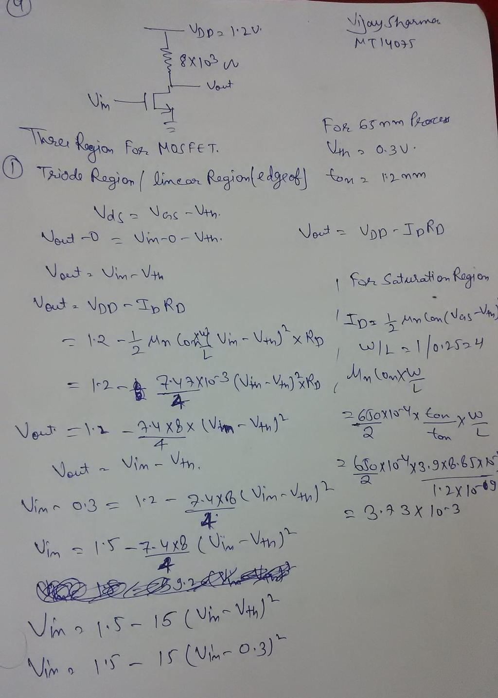
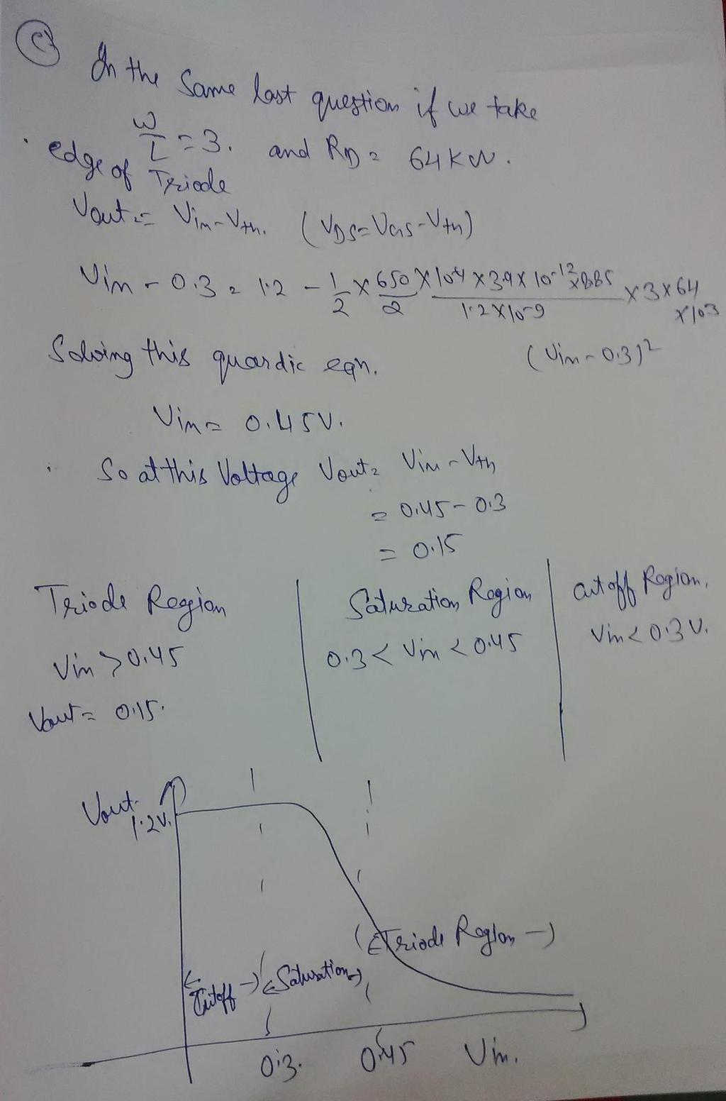
7 Where slope is -1. Voh=Vout = 1.06 V Vil=Vin= Where slope is 1 Vol=Vout=.129 Vin=0.68V Noise margin N low Noise Margin Nhigh 2. (a) Analyze and plot V out vs. V in with Vin varying from 0 to 1.2 volts (use steps of 0.25 V) for the MOS circuit shown below. Consider VDD= 1.2 V. (b) Repeat (a) using Cadence. c) Repeat (a) and (b) using a MOS transistor with (W/L) = 3/1. While doing so, vary the resistance values and report the results for 16K, 32K, and 64K Ohms. Is the discrepancy between manual and computer analysis larger or smaller (perform hand calculations for only resistance 64K)? Explain why. Also plot the voltage transfer characteristics and comment on noise margins. Can this circuit be used as an inverter? Solution: Using Cadence: firstly I do with 8K resistor and draw the transfer characteristics Schematic characteristic:

8 vgs i take Vgs and vds is equal to 1.2V and do simple analysis by which i can get transfer charcterstics of this circuit.

9 Transfer Characteristics for taking V out v/s V in taking Step Size of V in is 0.25: For question (c) change the width ratio by 3/1 mean width of NMOS is multiplied by 3. And take the resistor as a variable and varies it from 8 to 64 by taking times stepping of 2. So we get these types of transfer characteristics graph for 8K, 16K, 32K, 64K ohm resistor. also take Vds is taking in step size of As the resistance increases switching characteristics is decreases mean 64K is most away from its switching characteristics. As the resistance increases graph goes down. No this circuit can t be used as inverter because for 8K ohm resistor Vout does not goes to Zero. As the resistance increases Vout goes towards to zero. But not exact to be zero. So this circuit cannot behave like inverter.

10 (a).manual calculation of a and c part:
11

12 Max value of Vout=1.2V
13
ELEC 2210 EXPERIMENT 12 NMOS Logic
 ELEC 2210 EXPERIMENT 12 NMOS Logic Objectives: The experiments in this laboratory exercise will provide an introduction to NMOS logic. You will use the Bit Bucket breadboarding system to build and test
EE 230 Lab Lab 9. Prior to Lab
 MOS transistor characteristics This week we look at some MOS transistor characteristics and circuits. Most of the measurements will be done with our usual lab equipment, but we will also use the parameter
ECE 2274 MOSFET Voltmeter. Richard Cooper
 ECE 2274 MOSFET Voltmeter Richard Cooper Pre-Lab for MOSFET Voltmeter Voltmeter design: Build a MOSFET (2N7000) voltmeter in LTspice. The MOSFETs in the voltmeter act as switches. To turn on the MOSFET.
Design cycle for MEMS
 Design cycle for MEMS Design cycle for ICs IC Process Selection nmos CMOS BiCMOS ECL for logic for I/O and driver circuit for critical high speed parts of the system The Real Estate of a Wafer MOS Transistor
MOS TRANSISTOR THEORY
 MOS TRANSISTOR THEORY Introduction A MOS transistor is a majority-carrier device, in which the current in a conducting channel between the source and the drain is modulated by a voltage applied to the
ECE520 VLSI Design. Lecture 5: Basic CMOS Inverter. Payman Zarkesh-Ha
 ECE520 VLSI Design Lecture 5: Basic CMOS Inverter Payman Zarkesh-Ha Office: ECE Bldg. 230B Office hours: Wednesday 2:00-3:00PM or by appointment E-mail: pzarkesh@unm.edu Slide: 1 Review of Last Lecture
Learning Outcomes. Spiral 2-6. Current, Voltage, & Resistors DIODES
 26.1 26.2 Learning Outcomes Spiral 26 Semiconductor Material MOS Theory I underst why a diode conducts current under forward bias but does not under reverse bias I underst the three modes of operation
Improved Inverter: Current-Source Pull-Up. MOS Inverter with Current-Source Pull-Up. What else could be connected between the drain and V DD?
 Improved Inverter: Current-Source Pull-Up MOS Inverter with Current-Source Pull-Up What else could be connected between the drain and? Replace resistor with current source I SUP roc i D v IN v OUT Find
ENEE 307 Laboratory#2 (n-mosfet, p-mosfet, and a single n-mosfet amplifier in the common source configuration)
") Revised 2/16/2007 ENEE 307 Laboratory#2 (n-mosfet, p-mosfet, and a single n-mosfet amplifier in the common source configuration) *NOTE: The text mentioned below refers to the Sedra/Smith, 5th edition.
Revised 2/16/2007 ENEE 307 Laboratory#2 (n-mosfet, p-mosfet, and a single n-mosfet amplifier in the common source configuration) *NOTE: The text mentioned below refers to the Sedra/Smith, 5th edition.
EE 2274 MOSFET BASICS
 Pre Lab: Include your CN with prelab. EE 2274 MOSFET BASICS 1. Simulate in LTspice a family of output characteristic curves (cutve tracer) for the 2N7000 NMOS You will need to add the 2N7000 model to LTspice
Reading. Lecture 17: MOS transistors digital. Context. Digital techniques:
 Reading Lecture 17: MOS transistors digital Today we are going to look at the analog characteristics of simple digital devices, 5. 5.4 And following the midterm, we will cover PN diodes again in forward
8. Characteristics of Field Effect Transistor (MOSFET)
") 1 8. Characteristics of Field Effect Transistor (MOSFET) 8.1. Objectives The purpose of this experiment is to measure input and output characteristics of n-channel and p- channel field effect transistors
1 8. Characteristics of Field Effect Transistor (MOSFET) 8.1. Objectives The purpose of this experiment is to measure input and output characteristics of n-channel and p- channel field effect transistors
HW#3 Solution. Dr. Parker. Fall 2015
 HW#3 Solution Dr. Parker Fall 2015 Assume for the problems below that V dd = 1.8 V, V tp0 is -.7 V. and V tn0 is.7 V. V tpbodyeffect is -.9 V. and V tnbodyeffect is.9 V. Assume ß n (k n )= 219.4 W/L µ
EE 330 Laboratory 7 MOSFET Device Experimental Characterization and Basic Applications Spring 2017
 EE 330 Laboratory 7 MOSFET Device Experimental Characterization and Basic Applications Spring 2017 Objective: The objective of this laboratory experiment is to become more familiar with the operation of
HW#3 Solution. Dr. Parker. Fall 2014
 HW#3 Solution Dr. Parker Fall 2014 Assume for the problems below that V dd = 1.8 V, V tp0 is -.7 V. and V tn0 is.7 V. V tpbodyeffect is -.9 V. and V tnbodyeffect is.9 V. lambda=100 nm. Assume ß n (k n
Digital Electronics. Assign 1 and 0 to a range of voltage (or current), with a separation that minimizes a transition region. Positive Logic.
, with a separation that minimizes a transition region. Positive Logic.") Digital Electronics Assign 1 and 0 to a range of voltage (or current), with a separation that minimizes a transition region Positive Logic Logic 1 Negative Logic Logic 0 Voltage Transition Region Transition
Digital Electronics Assign 1 and 0 to a range of voltage (or current), with a separation that minimizes a transition region Positive Logic Logic 1 Negative Logic Logic 0 Voltage Transition Region Transition
Shorthand Notation for NMOS and PMOS Transistors
 Shorthand Notation for NMOS and PMOS Transistors Terminal Voltages Mode of operation depends on V g, V d, V s V gs = V g V s V gd = V g V d V ds = V d V s = V gs - V gd Source and drain are symmetric diffusion
EE5320: Analog IC Design
 EE5320: Analog IC Design Handout 3: MOSFETs Saurabh Saxena & Qadeer Khan Indian Institute of Technology Madras Copyright 2018 by EE6:Integrated Circuits & Systems roup @ IIT Madras Overview Transistors
ENEE307 Lab 7 MOS Transistors 2: Small Signal Amplifiers and Digital Circuits
 ENEE307 Lab 7 MOS Transistors 2: Small Signal Amplifiers and Digital Circuits In this lab, we will be looking at ac signals with MOSFET circuits and digital electronics. The experiments will be performed
EE105 Fall 2015 Microelectronic Devices and Circuits: MOSFET Prof. Ming C. Wu 511 Sutardja Dai Hall (SDH)
") EE105 Fall 2015 Microelectronic Devices and Circuits: MOSFET Prof. Ming C. Wu wu@eecs.berkeley.edu 511 Sutardja Dai Hall (SDH) 7-1 Simplest Model of MOSFET (from EE16B) 7-2 CMOS Inverter 7-3 CMOS NAND
EE105 Fall 2015 Microelectronic Devices and Circuits: MOSFET Prof. Ming C. Wu wu@eecs.berkeley.edu 511 Sutardja Dai Hall (SDH) 7-1 Simplest Model of MOSFET (from EE16B) 7-2 CMOS Inverter 7-3 CMOS NAND
Depletion-mode operation ( 공핍형 ): Using an input gate voltage to effectively decrease the channel size of an FET
: Using an input gate voltage to effectively decrease the channel size of an FET") Ch. 13 MOSFET Metal-Oxide-Semiconductor Field-Effect Transistor : I D D-mode E-mode V g The gate oxide is made of dielectric SiO 2 with e = 3.9 Depletion-mode operation ( 공핍형 ): Using an input gate voltage
Ch. 13 MOSFET Metal-Oxide-Semiconductor Field-Effect Transistor : I D D-mode E-mode V g The gate oxide is made of dielectric SiO 2 with e = 3.9 Depletion-mode operation ( 공핍형 ): Using an input gate voltage
1.2Vdc 1N4002. Anode V+
 ECE 2274 Pre-Lab for MOSFET Night Light and Voltmeter 1. Night Light The purpose of this part of experiment is to use the switching characteristics of the MOSFET to design a Night Light using a LED, MOSFET,
Lecture 16. Complementary metal oxide semiconductor (CMOS) CMOS 1-1
 CMOS 1-1") Lecture 16 Complementary metal oxide semiconductor (CMOS) CMOS 1-1 Outline Complementary metal oxide semiconductor (CMOS) Inverting circuit Properties Operating points Propagation delay Power dissipation
Lecture 16 Complementary metal oxide semiconductor (CMOS) CMOS 1-1 Outline Complementary metal oxide semiconductor (CMOS) Inverting circuit Properties Operating points Propagation delay Power dissipation
4.1 Device Structure and Physical Operation
 10/12/2004 4_1 Device Structure and Physical Operation blank.doc 1/2 4.1 Device Structure and Physical Operation Reading Assignment: pp. 235-248 Chapter 4 covers Field Effect Transistors ( ) Specifically,
Lecture 13 - Digital Circuits (II) MOS Inverter Circuits. October 25, 2005
 MOS Inverter Circuits. October 25, 2005") 6.12 - Microelectronic Devices and Circuits - Fall 25 Lecture 13-1 Lecture 13 - Digital Circuits (II) MOS Inverter Circuits October 25, 25 Contents: 1. NMOS inverter with resistor pull-up (cont.) 2. NMOS
6.12 - Microelectronic Devices and Circuits - Fall 25 Lecture 13-1 Lecture 13 - Digital Circuits (II) MOS Inverter Circuits October 25, 25 Contents: 1. NMOS inverter with resistor pull-up (cont.) 2. NMOS
University of Pittsburgh
 University of Pittsburgh Experiment #4 Lab Report MOSFET Amplifiers and Current Mirrors Submission Date: 07/03/2018 Instructors: Dr. Ahmed Dallal Shangqian Gao Submitted By: Nick Haver & Alex Williams
Basic Circuits. Current Mirror, Gain stage, Source Follower, Cascode, Differential Pair,
 Basic Circuits Current Mirror, Gain stage, Source Follower, Cascode, Differential Pair, CCS - Basic Circuits P. Fischer, ZITI, Uni Heidelberg, Seite 1 Reminder: Effect of Transistor Sizes Very crude classification:
MEASUREMENT AND INSTRUMENTATION STUDY NOTES UNIT-I
 MEASUREMENT AND INSTRUMENTATION STUDY NOTES The MOSFET The MOSFET Metal Oxide FET UNIT-I As well as the Junction Field Effect Transistor (JFET), there is another type of Field Effect Transistor available
ECEN 474/704 Lab 6: Differential Pairs
 ECEN 474/704 Lab 6: Differential Pairs Objective Design, simulate and layout various differential pairs used in different types of differential amplifiers such as operational transconductance amplifiers
UNIT 3: FIELD EFFECT TRANSISTORS
 FIELD EFFECT TRANSISTOR: UNIT 3: FIELD EFFECT TRANSISTORS The field effect transistor is a semiconductor device, which depends for its operation on the control of current by an electric field. There are
55:041 Electronic Circuits
 55:041 Electronic Circuits Mosfet Review Sections of Chapter 3 &4 A. Kruger Mosfet Review, Page-1 Basic Structure of MOS Capacitor Sect. 3.1 Width 1 10-6 m or less Thickness 50 10-9 m or less ` MOS Metal-Oxide-Semiconductor
Field Effect Transistors
 Field Effect Transistors LECTURE NO. - 41 Field Effect Transistors www.mycsvtunotes.in JFET MOSFET CMOS Field Effect transistors - FETs First, why are we using still another transistor? BJTs had a small
0.85V. 2. vs. I W / L
 EE501 Lab3 Exploring Transistor Characteristics and Design Common-Source Amplifiers Lab report due on September 22, 2016 Objectives: 1. Be familiar with characteristics of MOSFET such as gain, speed, power,
EE 501 Lab 1 Exploring Transistor Characteristics
 Objectives: Tasks: EE 501 Lab 1 Exploring Transistor Characteristics Lab report due on Sep 8th, 2011 1. Make sure you have your cadence 6 work properly 2. Familiar with characteristics of MOSFET such as
55:041 Electronic Circuits
 55:041 Electronic Circuits MOSFETs Sections of Chapter 3 &4 A. Kruger MOSFETs, Page-1 Basic Structure of MOS Capacitor Sect. 3.1 Width = 1 10-6 m or less Thickness = 50 10-9 m or less ` MOS Metal-Oxide-Semiconductor
ECEN3250 Lab 9 CMOS Logic Inverter
 Lab 9 CMOS Logic Inverter ECE Department University of Colorado, Boulder 1 Prelab Read Section 4.10 (4th edition Section 5.8), and the Lab procedure Do and turn in Exercise 4.41 (page 342) Do PSpice (.dc)
Field - Effect Transistor
 Page 1 of 6 Field - Effect Transistor Aim :- To draw and study the out put and transfer characteristics of the given FET and to determine its parameters. Apparatus :- FET, two variable power supplies,
3.CMOS Inverter-homework
 3.CMOS Inverter-homework 1. for a CMOS inverter, when the pmos and nmos are long-channel devices,or when the supply voltage is low, velocity does not occur, under these circumstances,vm(vin=vout)=? 2.
ECE520 VLSI Design. Lecture 2: Basic MOS Physics. Payman Zarkesh-Ha
 ECE520 VLSI Design Lecture 2: Basic MOS Physics Payman Zarkesh-Ha Office: ECE Bldg. 230B Office hours: Wednesday 2:00-3:00PM or by appointment E-mail: pzarkesh@unm.edu Slide: 1 Review of Last Lecture Semiconductor
EECS 312: Digital Integrated Circuits Lab Project 2 Extracting Electrical and Physical Parameters from MOSFETs. Teacher: Robert Dick GSI: Shengshuo Lu
 EECS 312: Digital Integrated Circuits Lab Project 2 Extracting Electrical and Physical Parameters from MOSFETs Teacher: Robert Dick GSI: Shengshuo Lu Due 3 October 1 Introduction In this lab project, we
Conduction Characteristics of MOS Transistors (for fixed Vds)! Topic 2. Basic MOS theory & SPICE simulation. MOS Transistor
! Topic 2. Basic MOS theory & SPICE simulation. MOS Transistor") Conduction Characteristics of MOS Transistors (for fixed Vds)! Topic 2 Basic MOS theory & SPICE simulation Peter Cheung Department of Electrical & Electronic Engineering Imperial College London (Weste&Harris,
Conduction Characteristics of MOS Transistors (for fixed Vds)! Topic 2 Basic MOS theory & SPICE simulation Peter Cheung Department of Electrical & Electronic Engineering Imperial College London (Weste&Harris,
Topic 2. Basic MOS theory & SPICE simulation
 Topic 2 Basic MOS theory & SPICE simulation Peter Cheung Department of Electrical & Electronic Engineering Imperial College London (Weste&Harris, Ch 2 & 5.1-5.3 Rabaey, Ch 3) URL: www.ee.ic.ac.uk/pcheung/
Conduction Characteristics of MOS Transistors (for fixed Vds) Topic 2. Basic MOS theory & SPICE simulation. MOS Transistor
 Topic 2. Basic MOS theory & SPICE simulation. MOS Transistor") Conduction Characteristics of MOS Transistors (for fixed Vds) Topic 2 Basic MOS theory & SPICE simulation Peter Cheung Department of Electrical & Electronic Engineering Imperial College London (Weste&Harris,
Conduction Characteristics of MOS Transistors (for fixed Vds) Topic 2 Basic MOS theory & SPICE simulation Peter Cheung Department of Electrical & Electronic Engineering Imperial College London (Weste&Harris,
Lecture 12 - Digital Circuits (I) The inverter. October 20, 2005
 The inverter. October 20, 2005") 6.12 - Microelectronic Devices and Circuits - Fall 25 Lecture 12-1 Lecture 12 - Digital Circuits (I) The inverter October 2, 25 Contents: 1. Introduction to digital electronics: the inverter 2. NMOS inverter
6.12 - Microelectronic Devices and Circuits - Fall 25 Lecture 12-1 Lecture 12 - Digital Circuits (I) The inverter October 2, 25 Contents: 1. Introduction to digital electronics: the inverter 2. NMOS inverter
! PN Junction. ! MOS Transistor Topology. ! Threshold. ! Operating Regions. " Resistive. " Saturation. " Subthreshold (next class)
") ESE370: ircuit-level Modeling, Design, and Optimization for Digital Systems Today! PN Junction! MOS Transistor Topology! Threshold Lec 7: September 16, 2015 MOS Transistor Operating Regions Part 1! Operating
ESE370: ircuit-level Modeling, Design, and Optimization for Digital Systems Today! PN Junction! MOS Transistor Topology! Threshold Lec 7: September 16, 2015 MOS Transistor Operating Regions Part 1! Operating
Three Terminal Devices
 Three Terminal Devices - field effect transistor (FET) - bipolar junction transistor (BJT) - foundation on which modern electronics is built - active devices - devices described completely by considering
EXPERIMENT # 1: REVERSE ENGINEERING OF INTEGRATED CIRCUITS Week of 1/17/05
 EXPERIMENT # 1: REVERSE ENGINEERING OF INTEGRATED CIRCUITS Week of 1/17/5 Experiment #1: Reading: Reverse engineering of integrated circuits Jaeger 9.2: MOS transistor layout and design rules HP4145 basics:
MOS Inverters Dr. Lynn Fuller Webpage:
 ROCHESTER INSTITUTE OF TECHNOLOGY MICROELECTRONIC ENGINEERING MOS Inverters Webpage: http://people.rit.edu/lffeee 82 Lomb Memorial Drive Rochester, NY 14623-5604 Tel (585) 475-2035 Email: Lynn.Fuller@rit.edu
EEC 118 Spring 2010 Lab #1: NMOS and PMOS Transistor Parameters
 EEC 118 Spring 2010 Lab #1: NMOS and PMOS Transistor Parameters Dept. of Electrical and Computer Engineering University of California, Davis March 18, 2010 Reading: Rabaey Chapter 3 [1]. Reference: Kang
Exam Below are two schematics of current sources implemented with MOSFETs. Which current source has the best compliance voltage?
 Exam 2 Name: Score /90 Question 1 Short Takes 1 point each unless noted otherwise. 1. Below are two schematics of current sources implemented with MOSFETs. Which current source has the best compliance
1. The simple, one transistor current source
 1. The simple, one transistor current source The test schematic (srs-simpla-mos.asc): 1. Design the NMOS source for a 40µA output current and the minimum allowed output voltage V omin =50mV. The design
HW#3 Solution. Dr. Parker. Spring 2014
 HW#3 olution r. Parker pring 2014 Assume for the problems below that V dd = 1.8 V, V tp0 is -.7 V. and V tn0 is.7 V. V tpbodyeffect is -.9 V. and V tnbodyeffect is.9 V. Assume ß n (k n )= 219.4 W/L µ A(microamps)/V
Lecture 11 Digital Circuits (I) THE INVERTER
 THE INVERTER") Lecture 11 Digital Circuits (I) THE INVERTER Outline Introduction to digital circuits The inverter NMOS inverter with resistor pull-up Reading Assignment: Howe and Sodini; Chapter 5, Sections 5.1-5.3 6.12
Lecture 11 Digital Circuits (I) THE INVERTER Outline Introduction to digital circuits The inverter NMOS inverter with resistor pull-up Reading Assignment: Howe and Sodini; Chapter 5, Sections 5.1-5.3 6.12
Electronic CAD Practical work. Week 1: Introduction to transistor models. curve tracing of NMOS transfer characteristics
 Electronic CAD Practical work Dr. Martin John Burbidge Lancashire UK Tel: +44 (0)1524 825064 Email: martin@mjb-rfelectronics-synthesis.com Martin Burbidge 2006 Week 1: Introduction to transistor models
ELEC 350L Electronics I Laboratory Fall 2012
 ELEC 350L Electronics I Laboratory Fall 2012 Lab #9: NMOS and CMOS Inverter Circuits Introduction The inverter, or NOT gate, is the fundamental building block of most digital devices. The circuits used
Module 4 : Propagation Delays in MOS Lecture 19 : Analyzing Delay for various Logic Circuits
 Module 4 : Propagation Delays in MOS Lecture 19 : Analyzing Delay for various Logic Circuits Objectives In this lecture you will learn the following Ratioed Logic Pass Transistor Logic Dynamic Logic Circuits
ECE2274 Pre-Lab for MOSFET logic LTspice NAND Gate, NOR Gate, and CMOS Inverter
 ECE2274 Pre-Lab for MOFET logic LTspice NAN ate, NOR ate, and CMO Inverter 1. NMO NAN ate Use Vdd = 9.. For the NMO NAN gate shown below gate, using the 2N7000 MOFET LTspice model such that Vto = 2.0.
Gechstudentszone.wordpress.com
 UNIT 4: Small Signal Analysis of Amplifiers 4.1 Basic FET Amplifiers In the last chapter, we described the operation of the FET, in particular the MOSFET, and analyzed and designed the dc response of circuits
Lecture 11 Circuits numériques (I) L'inverseur
 L'inverseur") Lecture 11 Circuits numériques (I) L'inverseur Outline Introduction to digital circuits The inverter NMOS inverter with resistor pull-up 6.12 Spring 24 Lecture 11 1 1. Introduction to digital circuits:
Lecture 11 Circuits numériques (I) L'inverseur Outline Introduction to digital circuits The inverter NMOS inverter with resistor pull-up 6.12 Spring 24 Lecture 11 1 1. Introduction to digital circuits:
CPE/EE 427, CPE 527 VLSI Design I CMOS Inverter. CMOS Inverter: A First Look
 CPE/EE 427, CPE 527 VLSI Design I CMOS Inverter Department of Electrical and Computer Engineering University of Alabama in Huntsville Aleksandar Milenkovic CMOS Inverter: A First Look C L 9/11/26 VLSI
UNIT-1 Bipolar Junction Transistors. Text Book:, Microelectronic Circuits 6 ed., by Sedra and Smith, Oxford Press
 UNIT-1 Bipolar Junction Transistors Text Book:, Microelectronic Circuits 6 ed., by Sedra and Smith, Oxford Press Figure 6.1 A simplified structure of the npn transistor. Microelectronic Circuits, Sixth
C H A P T E R 5. Amplifier Design
 C H A P T E 5 Amplifier Design The Common-Source Amplifier v 0 = r ( g mvgs )( D 0 ) A v0 = g m r ( D 0 ) Performing the analysis directly on the circuit diagram with the MOSFET model used implicitly.
Short Channel Bandgap Voltage Reference
 Short Channel Bandgap Voltage Reference EE-584 Final Report Authors: Thymour Legba Yugu Yang Chris Magruder Steve Dominick Table of Contents Table of Figures... 3 Abstract... 4 Introduction... 5 Theory
ECE315 / ECE515 Lecture 9 Date:
 Lecture 9 Date: 03.09.2015 Biasing in MOS Amplifier Circuits Biasing using Single Power Supply The general form of a single-supply MOSFET amplifier biasing circuit is: We typically attempt to satisfy three
INTRODUCTION TO ELECTRONICS EHB 222E
 INTRODUCTION TO ELECTRONICS EHB 222E MOS Field Effect Transistors (MOSFETS II) MOSFETS 1/ INTRODUCTION TO ELECTRONICS 1 MOSFETS Amplifiers Cut off when v GS < V t v DS decreases starting point A, once
Lecture 4. MOS transistor theory
 Lecture 4 MOS transistor theory 1.7 Introduction: A MOS transistor is a majority-carrier device, in which the current in a conducting channel between the source and the drain is modulated by a voltage
BJT Amplifier. Superposition principle (linear amplifier)
") BJT Amplifier Two types analysis DC analysis Applied DC voltage source AC analysis Time varying signal source Superposition principle (linear amplifier) The response of a linear amplifier circuit excited
BJT Amplifier Two types analysis DC analysis Applied DC voltage source AC analysis Time varying signal source Superposition principle (linear amplifier) The response of a linear amplifier circuit excited
Metal Oxide Semiconductor Field-Effect Transistors (MOSFETs)
") Metal Oxide Semiconductor Field-Effect Transistors (MOSFETs) Device Structure N-Channel MOSFET Providing electrons Pulling electrons (makes current flow) + + + Apply positive voltage to gate: Drives away
Metal Oxide Semiconductor Field-Effect Transistors (MOSFETs) Device Structure N-Channel MOSFET Providing electrons Pulling electrons (makes current flow) + + + Apply positive voltage to gate: Drives away
Experiment 5 Single-Stage MOS Amplifiers
 Experiment 5 Single-Stage MOS Amplifiers B. Cagdaser, H. Chong, R. Lu, and R. T. Howe UC Berkeley EE 105 Fall 2005 1 Objective This is the first lab dealing with the use of transistors in amplifiers. We
Chapter 6 DIFFERENT TYPES OF LOGIC GATES
 Chapter 6 DIFFERENT TYPES OF LOGIC GATES Lesson 9 CMOS gates Ch06L9-"Digital Principles and Design", Raj Kamal, Pearson Education, 2006 2 Outline CMOS (n-channel based MOSFETs based circuit) CMOS Features
Bring your textbook to lab.
 Bring your textbook to lab. Electrical & Computer Engineering Department ECE 2100 Experiment No. 11 Introduction to MOSFET Transistors A. Stolp, 4/3/01 rev,4/6/03 Minimum required points = 46 Recommend
ECE4902 C2012 Lab 3. Qualitative MOSFET V-I Characteristic SPICE Parameter Extraction using MOSFET Current Mirror
 ECE4902 C2012 Lab 3 Qualitative MOSFET VI Characteristic SPICE Parameter Extraction using MOSFET Current Mirror The purpose of this lab is for you to make both qualitative observations and quantitative
ECE/CoE 0132: FETs and Gates
 ECE/CoE 0132: FETs and Gates Kartik Mohanram September 6, 2017 1 Physical properties of gates Over the next 2 lectures, we will discuss some of the physical characteristics of integrated circuits. We will
Submission date: Wednesday 21/3/2018
 Faculty of Information Engineering & Technology Electrical & Electronics Department Course: Microelectronics Lab ELCT605 Spring 2018 Dr. Eman Azab Eng. Samar Shukry Analog Report 1, 2 DC, TRANSIENT, AND
EE 42/100 Lecture 23: CMOS Transistors and Logic Gates. Rev A 4/15/2012 (10:39 AM) Prof. Ali M. Niknejad
 Prof. Ali M. Niknejad") A. M. Niknejad University of California, Berkeley EE 100 / 42 Lecture 23 p. 1/16 EE 42/100 Lecture 23: CMOS Transistors and Logic Gates ELECTRONICS Rev A 4/15/2012 (10:39 AM) Prof. Ali M. Niknejad University
A. M. Niknejad University of California, Berkeley EE 100 / 42 Lecture 23 p. 1/16 EE 42/100 Lecture 23: CMOS Transistors and Logic Gates ELECTRONICS Rev A 4/15/2012 (10:39 AM) Prof. Ali M. Niknejad University
Chapter 6 DIFFERENT TYPES OF LOGIC GATES
 Chapter 6 DIFFERENT TYPES OF LOGIC GATES Lesson 8 NMOS gates Ch06L8-"Digital Principles and Design", Raj Kamal, Pearson Education, 2006 2 Outline NMOS (n-channel based MOSFETs based circuit) NMOS Features
Introduction to Electronic Devices
 Introduction to Electronic Devices (Course Number 300331) Fall 2006 Dr. Dietmar Knipp Assistant Professor of Electrical Engineering Information: http://www.faculty.iubremen.de/dknipp/ Source: Apple Ref.:
Study of Differential Amplifier using CMOS
 Study of Differential Amplifier using CMOS Mr. Bhushan Bangadkar PG Scholar Mr. Amit Lamba Assistant Professor Mr. Vipin Bhure Assistant Professor Electronics and Communication Electronics and Communication
CHAPTER 8 FIELD EFFECT TRANSISTOR (FETs)
") CHAPTER 8 FIELD EFFECT TRANSISTOR (FETs) INTRODUCTION - FETs are voltage controlled devices as opposed to BJT which are current controlled. - There are two types of FETs. o Junction FET (JFET) o Metal
CHAPTER 8 FIELD EFFECT TRANSISTOR (FETs) INTRODUCTION - FETs are voltage controlled devices as opposed to BJT which are current controlled. - There are two types of FETs. o Junction FET (JFET) o Metal
ECEN 474/704 Lab 5: Frequency Response of Inverting Amplifiers
 ECEN 474/704 Lab 5: Frequency Response of Inverting Amplifiers Objective Design, simulate and layout various inverting amplifiers. Introduction Inverting amplifiers are fundamental building blocks of electronic
CMOS Transistor and Circuits. Jan 2015 CMOS Transistor 1
 CMOS Transistor and Circuits Jan 2015 CMOS Transistor 1 Latchup in CMOS Circuits Jan 2015 CMOS Transistor 2 Parasitic bipolar transistors are formed by substrate and source / drain devices Latchup occurs
Solution HW4 Dr. Parker EE477
 Solution HW4 Dr. Parker EE477 Assume for the problems below that V dd = 1.8 v, V tp0 is -.7 v. and V tn0 is.7 V. V tpbodyeffect is -.9 v. and V tnbodyeffect is.9 V. Assume ß n (k n )= 219.4 W/L µ A(microamps)/V
444 Index. F Fermi potential, 146 FGMOS transistor, 20 23, 57, 83, 84, 98, 205, 208, 213, 215, 216, 241, 242, 251, 280, 311, 318, 332, 354, 407
 Index A Accuracy active resistor structures, 46, 323, 328, 329, 341, 344, 360 computational circuits, 171 differential amplifiers, 30, 31 exponential circuits, 285, 291, 292 multifunctional structures,
Microelectronics Circuit Analysis and Design. MOS Capacitor Under Bias: Electric Field and Charge. Basic Structure of MOS Capacitor 9/25/2013
 Microelectronics Circuit Analysis and Design Donald A. Neamen Chapter 3 The Field Effect Transistor In this chapter, we will: Study and understand the operation and characteristics of the various types
Common-Source Amplifiers
 Lab 2: Common-Source Amplifiers Introduction The common-source stage is the most basic amplifier stage encountered in CMOS analog circuits. Because of its very high input impedance, moderate-to-high gain,
Laboratory #9 MOSFET Biasing and Current Mirror
 Laboratory #9 MOSFET Biasing and Current Mirror. Objectives 1. Review the MOSFET characteristics and transfer function. 2. Understand the relationship between the bias, the input signal and the output
Curve Tracer Laboratory Assistant Using the Analog Discovery Module as A Curve Tracer
 Curve Tracer Laboratory Assistant Using the Analog Discovery Module as A Curve Tracer The objective of this lab is to become familiar with methods to measure the dc current-voltage (IV) behavior of diodes
Homework Assignment 07
 Homework Assignment 07 Question 1 (Short Takes). 2 points each unless otherwise noted. 1. A single-pole op-amp has an open-loop low-frequency gain of A = 10 5 and an open loop, 3-dB frequency of 4 Hz.
ECE380 Digital Logic. Logic values as voltage levels
 ECE380 Digital Logic Implementation Technology: NMOS and PMOS Transistors, CMOS logic gates Dr. D. J. Jackson Lecture 13-1 Logic values as voltage levels V ss is the minimum voltage that can exist in the
ECE 546 Lecture 12 Integrated Circuits
 ECE 546 Lecture 12 Integrated Circuits Spring 2018 Jose E. Schutt-Aine Electrical & Computer Engineering University of Illinois jesa@illinois.edu ECE 546 Jose Schutt Aine 1 Integrated Circuits IC Requirements
Microelectronics, BSc course
 Microelectronics, BSc course MOS inverters http://www.eet.bme.hu/~poppe/miel/en/13-mosfet2.pptx http://www.eet.bme.hu Overview of MSOFET types 13-11-2014 Microelectronics BSc course, MOS inverters András
Design and Simulation of Low Voltage Operational Amplifier
 Design and Simulation of Low Voltage Operational Amplifier Zach Nelson Department of Electrical Engineering, University of Nevada, Las Vegas 4505 S Maryland Pkwy, Las Vegas, NV 89154 United States of America
Week 9a OUTLINE. MOSFET I D vs. V GS characteristic Circuit models for the MOSFET. Reading. resistive switch model small-signal model
 Week 9a OUTLINE MOSFET I vs. V GS characteristic Circuit models for the MOSFET resistive switch model small-signal model Reading Rabaey et al.: Chapter 3.3.2 Hambley: Chapter 12 (through 12.5); Section
EECE 481. MOS Basics Lecture 2
 EECE 481 MOS Basics Lecture 2 Reza Molavi Dept. of ECE University of British Columbia reza@ece.ubc.ca Slides Courtesy : Dr. Res Saleh (UBC), Dr. D. Sengupta (AMD), Dr. B. Razavi (UCLA) 1 PN Junction and
Lecture 13 - Digital Circuits (II) MOS Inverter Circuits. March 22, 2001
 MOS Inverter Circuits. March 22, 2001") 6.12 - Microelectronic Devices and Circuits - Spring 21 Lecture 13-1 Lecture 13 - Digital Circuits (II) MOS Inverter Circuits March 22, 21 Contents: 1. NMOS inverter with resistor pull-up (cont.) 2. NMOS
6.12 - Microelectronic Devices and Circuits - Spring 21 Lecture 13-1 Lecture 13 - Digital Circuits (II) MOS Inverter Circuits March 22, 21 Contents: 1. NMOS inverter with resistor pull-up (cont.) 2. NMOS
Electronic Circuits for Mechatronics ELCT 609 Lecture 6: MOS-FET Transistor
 Electronic Circuits for Mechatronics ELCT 609 Lecture 6: MOS-FET Transistor Assistant Professor Office: C3.315 E-mail: eman.azab@guc.edu.eg 1 Introduction Why we call it Transistor? The name came as an
Chapter 5: Field Effect Transistors
 Chapter 5: Field Effect Transistors Slide 1 FET FET s (Field Effect Transistors) are much like BJT s (Bipolar Junction Transistors). Similarities: Amplifiers Switching devices Impedance matching circuits
Field Effect Transistors (FET s) University of Connecticut 136
 University of Connecticut 136") Field Effect Transistors (FET s) University of Connecticut 136 Field Effect Transistors (FET s) FET s are classified three ways: by conduction type n-channel - conduction by electrons p-channel - conduction
Field Effect Transistors (FET s) University of Connecticut 136 Field Effect Transistors (FET s) FET s are classified three ways: by conduction type n-channel - conduction by electrons p-channel - conduction
A COMPARATIVE ANALYSIS OF 180 NM PROCESS CMOS INVERTER
 A COMPARATIVE ANALYSIS OF 180 NM PROCESS CMOS INVERTER Amresh Kumar Lenka Department of Electronics and Communication Engineering Centre for Advance Post Graduate Studies, Rourkela Ananya Dastidar Biju
! Review: MOS IV Curves and Switch Model. ! MOS Device Layout. ! Inverter Layout. ! Gate Layout and Stick Diagrams. ! Design Rules. !
 ESE 570: Digital Integrated Circuits and VLSI Fundamentals Lec 3: January 21, 2016 MOS Fabrication pt. 2: Design Rules and Layout Lecture Outline! Review: MOS IV Curves and Switch Model! MOS Device Layout!