WIDE-RANGE 7-SWITCH FLYING CAPACITOR BASED DC-DC CONVERTER FOR POINT-OF-LOAD APPLICATIONS
|
|
|
- Edmund Wood
- 5 years ago
- Views:
Transcription
1 WIDE-RANGE 7-SWITCH FLYING CAPACITOR BASED DC-DC CONVERTER FOR POINT-OF-LOAD APPLICATIONS By Parh Jain A hesis submied in conformiy wih he requiremens for he degree of Maser of Applied Science Graduae Deparmen of Elecrical and Compuer Engineering Universiy of Torono Copyrigh by Parh Jain 2015
2 WIDE-RANGE 7-SWITCH DC-DC CONVERTER FOR POINT-OF-LOAD APPLICATIONS Parh Jain Maser of Applied Science Graduae Deparmen of Elecrical and Compuer Engineering Universiy of Torono 2015 ABSTRACT In his hesis a dc-dc converer referred o as he 7-swich flying capacior (7SFC) based muli-level buck converer inended for poin-of-load applicaions is presened. The 7SFC operaes wih he principle of ransformabiliy which allows i o run in several swiching modes when paired wih a digial conroller. The mode is seleced based on inpu and oupu condiions by esimaing he highes efficiency mode. The 7SFC converer uilizes a flying capacior, which for cerain modes allows for a large reducion in swiching losses, especially when he converer is operaed wih highinpu volages. Compared o he convenional 2-phase inerleaved buck converer, he 7SFC is able o reduce he size of he oupu inducors and capacior by 33%. The 7SFC discree prooype is able o achieve efficiencies greaer han 90% over he majoriy of he operaing range. ii
3 ACKNOWLEDGEMENTS I would firs like o offer my graiude o he Universiy of Torono and he saff and faculy of he Deparmen of Elecrical and Engineering for providing a comforable and friendly environmen o perform my research over he pas wo years. I would also like o hank Alex Gerfer and Marin Haug of Wurh Elekronik for financially supporing my degree and providing useful feedback hrough he compleion of my projec. Mos of all, I would like o sincerely hank Prof. Aleksandar Prodic for his compassionae suppor hrough boh my undergraduae and graduae sudies. Prof. Prodic has gone beyond he call of duy on many occasions o provide me wih opporuniies o shine in he discipline and perform valuable research. Also, I would like o hank him for he many meaningful personal and professional connecions he has provided me wih. Finally, I would like o hank all of my lab maes who I have had he greaes pleasures of working wih over he course of my degree. Special hanks go ou o: Nenad Vukadinovic, Tim McRae, SM Ahsannuzaman, Behzad Mahdavikkah, Mahmoud Shousha, Amr Amin, Adrian Sraka, Jordan Kis, Jusin Blackman, Maryam Amouzandeh, Shadi Dashmiz and anyone who I have forgoen o menion here. Wihou heir company and suppor he lab environmen would no have been he same. iii
4 TABLE OF CONTENTS Chaper 1: Inroducion Poin-of-Load Converers Thesis Objecive Thesis Ouline... 3 Chaper 2: Prior Ar in Non-Isolaed Poin-of-Load Conversion Non-Isolaed Poin-of-Load Converer Topologies Phase Inerleaved Buck Converer Double Sep-Down Buck Converer Phase 3-Level Buck Digial Conrol Chaper 3: Novel Flying Capacior Based Dc-dc Topology Principle of Operaion SFC: 2-Phase Inerleaved Buck Mode Operaion SFC: High Sep-Down Mode Operaion SFC: 3-Level Buck Mode Operaion Digial Conroller for he 7SFC Converer Loss Breakdown Conducion Losses Swiching Losses MOSFET Oupu Capacior Losses Gae Drive Losses Reverse Recovery Losses Inducor Core Loss Volume Esimaion Phase Shedding iv
5 3.5 Gae Driving Chaper 4: Experimenal Resuls and Comparison Reacive Componen Selecion and Volume Comparison Inducor Selecion Oupu Capacior Selecion Volume Comparison Power Loss Breakdown High Sep-Down Raio Loss Breakdown Medium Sep-Down Raio Loss Breakdown Loss Breakdown for Sep Down Raio Close o SFC Seady-Sae Operaion SFC: High Sep-Down Mode Waveforms SFC: Inerleaved Buck Mode Waveforms SFC: 3-Level Buck Mode Waveforms Convenional Inerleaved Buck Converer Waveforms Efficiency Resuls and Comparison Chaper 5: Conclusions and Fuure Work Major Accomplishmens Fuure Work References Appendix A: A. 2-Phase 3-Level Buck Converer Operaion for M > Appendix B: B. 7SFC Converer Conducion Losses B.1 Inerleaved Buck Mode B.2 High Sep-Down Mode v
6 B.3 3-Level Buck Mode Appendix C: C. Adding RMS Currens Appendix D: D. 2-Phase Inerleaved Buck Converer Loss Breakdown D.1 Conducion Losses D.2 Swiching Losses D.3 MOSFET Oupu Capacior Losses D.4 Gae Drive Losses D.5 Reverse Recovery Losses D.6 Inducor Core Loss Appendix E: E. Addiional Experimenal Seady-Sae Waveforms E.1 7SFC: High Sep-Down Mode Waveforms E.2 7SFC: Inerleaved Buck Mode E.3 7SFC 3-level buck mode E.4 Convenional Inerleaved Buck Converer Appendix F: F. Addiional Experimenal Efficiency Resuls vi
7 LIST OF TABLES Table 1. Experimenal Prooype Componens Table 2. Oupu capacior selecion based on oupu volage ripple Table 3. Oupu capacior selecion based on oupu volage deviaion Table 4. Toal silicon area comparison based on maximum inpu volage, V in,max vii
8 LIST OF FIGURES Figure 1-1: Inermediae bus power archiecure for poin-of-load applicaions... 2 Figure 2-1: Prior ar in non-isolaed poin-of-load conversion. a) Inerleaved buck converer, b) Double sep-down buck converer, c) 2-phase 3-level buck converer... 6 Figure 2-2: Swiching sequence and inducor waveforms for he inerleaved buck converer for D< Figure 2-3: Swiching sequence and inducor waveforms for he double sep-down buck converer.. 9 Figure 2-4: DC equivalen circui for he double sep-down buck converer Figure 2-5: Swiching sequence and inducor waveforms for he 2-phase 3-level buck converer operaing in he M<0.5 mode Figure 3-1: Four quadrans of he operaing range Figure 3-2: Prior ar caegorized ino he four quadrans of he operaing range Figure 3-3: Novel 7-swich flying capacior (7SFC) based muli-level buck converer Figure 3-4: Swiching sequence and inducor waveforms for he inerleaved buck mode of he 7SFC converer operaing wih D< Figure 3-5: Swiching sequence and inducor waveforms for he inerleaved buck mode of he 7SFC converer operaing wih D> Figure 3-6: Swiching sequence and inducor waveforms for he high sep-down mode of he 7SFC converer Figure 3-7: Swiching sequence and inducor waveforms for he 3-level buck mode of he 7SFC converer Figure 3-8: Volage mode conroller for he 7SFC converer viii
9 Figure 3-9: Oupu capacior posiive charge for oupu volage ripple calculaion Figure 3-10: Swiching sequence and inducor waveforms for he single-phase inerleaved buck operaion of he 7SFC converer Figure 3-11: Swiching sequence and inducor waveforms for he single-phase 3-level buck operaion of he 7SFC converer Figure 3-12: Gae driving implemenaion of he 7SFC converer, a) charging of SW 5 boosrap circui, b) charging of SW 1 and SW 4 boosrap circuis Figure 4-1: Image of he op view of he experimenal prooype. The op PCB consiss of he power sage and he boom PCB is he conrol board wih sensing, ADCs and DACs Figure 4-2: Power loss breakdown for Vin=24V & Vou=1V, a) inerleaved buck converer, b) 7SFC converer Figure 4-3: Power loss breakdown for V in =7V & V ou =1V, a) inerleaved buck converer, b) 7SFC converer Figure 4-4: Power loss breakdown for V in =12V & V ou =5V, a) inerleaved buck converer, b) 7SFC converer, 3-level buck mode, c) 7SFC converer, inerleaved buck mode Figure 4-5: Experimenal waveforms for he 7SFC converer operaing in he high sep-down mode wih V in =12V & V ou =1V, a) displaying swiching nodes v x1 and v x2, b) displaying swiching node v x1 and oupu volage v ou Figure 4-6: Experimenal waveforms for he 7SFC converer operaing in he inerleaved buck mode wih V in =24V & V ou =12V, a) displaying swiching nodes v x1 and v x2, b) displaying swiching node v x1 and oupu volage v ou Figure 4-7: Experimenal waveforms for he 7SFC converer operaing in he 3-level buck mode wih V in =36V & V ou =12V, displaying swiching node v x and oupu volage v ou ix
10 Figure 4-8: Experimenal waveforms for he convenional inerleaved buck converer wih V in =12V & V ou =1V, a) displaying swiching nodes v x1 and v x2, b) displaying swiching node v x1 and oupu volage v ou Figure 4-9: Experimenal waveforms for he convenional inerleaved buck converer wih V in =36V & V ou =12V, a) displaying swiching nodes v x1 and v x2, b) displaying swiching node v x1 and oupu volage v ou Figure 4-10: Efficiency curves for V in =12V &V ou =1V for, a) convenional inerleaved buck converer, b) 7SFC converer Figure 4-11: Efficiency curves for V in =12V & V ou =5V for, a) inerleaved buck converer, b) 7SFC converer Figure 4-12: Efficiency curves for V in =15V & V ou =12V for, a) inerleaved buck converer, b) 7SFC converer Figure 5-1: Modes of he 7SFC converer caegorized based on he operaing range Figure A-1: Swiching sequence and inducor waveforms for he 2-phase 3-level buck converer operaing in he M>0.5 mode Figure B-1: Swiching sequence and inducor waveforms for he inerleaved buck mode of he 7SFC converer for a) D<0.5 and b) D> Figure B-2: Swiching sequence and inducor waveforms for he high sep-down mode of he 7SFC converer Figure B-3: Curren division during synchronous recificaion for he high sep-down mode of he 7SFC converer Figure B-4: Inducor and swich currens for he 3-level buck mode of he 7SFC converer Figure C-1: Typical inducor curren waveform Figure D-1: Inducor and swich currens for he inerleaved buck converer x
11 Figure E-1: Experimenal waveforms for he high sep-down mode of he 7SFC converer wih V in =48V & V ou =3.3V Figure E-2: Experimenal waveforms for he high sep-down mode of he 7SFC converer wih V in =48V & V ou =11V Figure E-3: Experimenal waveforms for he inerleaved buck mode of he 7SFC converer wih V in =15V & V ou =12V Figure E-4: Experimenal waveforms for he inerleaved buck mode of he 7SFC converer wih V in =6V & V ou =5V Figure E-5: Experimenal waveforms for he 3-level buck mode of he 7SFC converer wih V in =48V & V ou =12V Figure E-6: Experimenal waveforms for he 3-level buck mode of he 7SFC converer wih V in =5V & V ou =3.3V Figure E-7: Experimenal waveforms for he convenional inerleaved buck converer wih V in =48V & V ou =3.3V Figure E-8: Experimenal waveforms for he convenional inerleaved buck converer wih V in =48V & V ou =12V Figure E-9: Experimenal waveforms for he convenional inerleaved buck converer wih V in =24V & V ou =12V Figure E-10: Experimenal waveforms for he convenional inerleaved buck converer wih V in =15V & V ou =12V Figure E-11: Experimenal waveforms for he convenional inerleaved buck converer wih V in =6V & V ou =5V Figure E-12: Experimenal waveforms for he convenional inerleaved buck converer wih V in =15V & V ou =3.3V Figure F-1: Efficiency curves for he 7SFC converer wih V ou =1V xi
12 Figure F-2: Efficiency curves for he 7SFC converer wih Vou=3.3V Figure F-3: Efficiency curves for he 7SFC converer wih V ou =5V Figure F-4: Efficiency curves for he 7SFC converer wih V ou =12V xii
13 1 CHAPTER 1: 1. INTRODUCTION In almos all elecronics oday, poin-of-load (PoL) dc-dc converers are needed o provide regulaed dc volages o various funcional blocks in a sysem. Generally, hese funcional blocks require differen volage and power levels and, herefore, dedicaed PoL converers are used for each block. For hese sysems, cusom designs of he buck converer are almos exclusively used as he PoL of choice. The use of cusom PoL designs allows he designer o maximize efficiency and minimize volume for each converer, and opimize he full sysem performance. However, his increases sysem-level design complexiy, could influence reliabiliy, and increases manufacuring cos [1]. For example, o design, verify and implemen up o 10 dedicaed PoLs would heavily burden he designer and increase he ime-o-marke significanly. For hese reasons, i is beneficial o have a sand-alone wide-range universal converer ha can provide a large range of volages and power levels suiable for all applicaions, raher han specific ones. For many applicaions he success of a PoL is deermined by is abiliy o provide a regulaed volage and power wih high power processing efficiency, low volume, and good dynamic performance. The main objecive of his hesis is o propose a opology ha will ac as he aforemenioned universal converer and mee he necessary requiremens for wide-range PoL applicaions. 1.1 Poin-of-Load Converers Poin-of-load converers are used expansively in elecronic sysems o efficienly disribue power o all of he necessary loads, from communicaions and compuer applicaions o medical and miliary areas. PoLs are dc-dc converers ha are placed close o he loads hey are supplying power o, and provide conversion, regulaion and in some cases isolaion [2]. A diagram of he inermediae bus power archiecure is presened in Figure 1-1. In his sysem, an ac-dc fron-end converer is uilized o provide basic isolaion and conversion o a high-volage bus (generally 48V o 380V). Following his, an isolaed dc-dc converer is used o supply an inermediae bus a a lower volage (ypically 3.3V o 48V) from which he PoLs operae. This power archiecure
14 2 has gained populariy over he las fifeen years and is he main archiecure for poin-of-load sysems [3]. Inermediae bus volages are heavily ied o paricular applicaions: 8V or 12V for he communicaions segmen, 12V and 24V for compuer sysems, 3.3V, 5V, 12V and 48V for medical, and volages even higher for miliary and aerospace applicaions [4]. Since isolaion is already provided by he previous conversion sages, he PoLs can be non-isolaed. AC Power ( 90V o 265V ) AC-DC Fron-End Converer High Volage Bus ( 48V o 380V ) Isolaed Inermediae Bus Converer Inermediae Bus ( 3.3V o 48V ) Non-Isolaed POL Non-Isolaed POL Non-Isolaed POL Non-Isolaed POL 1V 3.3V 5V 12V Figure 1-1: Inermediae bus power archiecure for poin-of-load applicaions According o marke research performed by Darnell [4,5], he oal marke revenue for dc-dc converer modules in 2016 is expeced o be $4.3 billion and, for dc-dc converer IC soluions, he marke sales are expeced o be 32 billion unis; boh being rapidly growing markes. Paricular aenion in he sudies is given o he non-isolaed PoL applicaion segmen where he inermediae bus power archiecure has gained populariy due o increased sysem performance. The growh of his marke segmen relies on he improvemens of PoL converers compared o he convenional buck soluion. By increasing power processing efficiency, lowering cos, reducing size, and improving configurabiliy, he use of he PoL can be expanded. In a convenional PoL sysem each non-isolaed PoL block in Figure 1-1 would be a cusom buck converer designed based on he inermediae bus volage and required oupu volage and power. In a large sysem, he design complexiy increases direcly wih he number of required PoLs.
15 3 Anoher drawback of he convenional buck soluion is he dependence of sysem performance on he inpu and oupu operaing condiions. For high inermediae bus volages, he power processing efficiency of he buck converer significanly degrades. Due o hese limiaions, he focus of his hesis will be on he design of a novel non-isolaed PoL converer ha can operae for a wide range of operaing condiions wih high power processing efficiency and low volume compared o he convenional buck converer. 1.2 Thesis Objecive The objecive of his hesis is o analyze he limiaions of exising PoL soluions and o propose a new soluion ha can improve on hem. The specific limiaions ha are being addressed are wide-range conversion, overall volume and power processing efficiency. This is done by inroducing a novel non-isolaed opology ha uilizes specific advanages of several pre-exising opologies and combining hem ino a single low-volume high-efficiency converer. Compared o he convenionally used 2-phase inerleaved buck converer, his new opology improves in he following ways: Taking advanage of muli-level dc-dc conversion Muli-mode converer operaion for efficiency opimizaion Significan reducion in reacive componen volume Reducing silicon area needed for implemenaion 1.3 Thesis Ouline The maerial of his hesis is presened in he following sequence: In Chaper 2 pre-exising opologies for non-isolaed PoL applicaions are presened. These opologies include he convenional 2-phase inerleaved buck converer, as well as previously proposed alernaives, he double sep-down buck [6] and he 3-level buck converer [7]. The opology limiaions are discussed, clearly saing specific areas of improvemen, which are addressed in Chaper 3 wih he inroducion of he new opology. Following his discussion, prior ar for conrol is presened including digial conrol echniques for dc-dc converers.
16 4 Chaper 3 begins by oulining he design sraegy used o come up wih he novel 7-swich flying capacior (7SFC) based muli-level buck converer. Then, he principle of operaion and full analyses of converer losses and volume esimaions are presened. Conrol echniques are discussed for he 7SFC converer and he conroller complexiy is analyzed. In Chaper 4 an experimenal prooype ha was designed, buil and esed is inroduced wih he following specificaions: 3V < V in < 48V, 1V < V ou < 12V, I load < 6A. Power loss breakdowns for he 7SFC converer and he convenional inerleaved buck converer are compared over his operaing range. Efficiency resuls for he 7SFC muli-level buck are presened for many operaing poins. The volume comparison for reacive componens is verified hrough inducor curren ripple and ransien comparisons. The hesis conclusion as well as possible fuure work wih regards o he 7SFC muli-level buck converer is presened in Chaper 5.
17 5 CHAPTER 2: 2. PRIOR ART IN NON-ISOLATED POINT-OF-LOAD CONVERSION This secion is a review of he convenional and previously proposed echnologies for nonisolaed poin-of-load conversion in erms of boh opologies and complemenary conrol mehods. Single-sage opologies are preferred for his applicaion due o he design simpliciy, and he efficiency improvemens by neglecing a fron-end conversion sage. Firs, hree opologies will be examined as background in non-isolaed PoL opologies, he 2-phase inerleaved buck converer, he double sep-down buck converer [6], and he 2-phase 3-level buck converer [7]. In he second par of his secion digial conrol mehods are discussed as a means of conrolling PoLs. 2.1 Non-Isolaed Poin-of-Load Converer Topologies The buck converer opology is he mos widely used opology for non-isolaed PoLs due o he exensive research wih regards o is design and conrol [8]. Also, o improve on he buck converer s performance, many opologies and conrol mehods have been derived o opimize efficiency for paricular applicaions of PoLs [9-13]. In hese opologies, he rade-off for design simpliciy over flexibiliy for a wide range of conversion raios is made. Muli-level converers have also been adoped for high-power converers [7], and recenly proposed for low-power applicaions as well [14]. Muli-level opologies have gained aenion over recen years due o heir improvemens in efficiency and volume over convenional buck opologies a he cos of added design complexiy. Three opologies will be discussed in his secion as a review of prior ar in non-isolaed PoL conversion, 1) he 2-phase inerleaved buck, 2) he double sep-down buck proposed by Nishijima [6] and 3) he 2-phase 3-level buck converer, whose single-phase counerpar was proposed by Meynard [7]. The hree opologies are shown in Figure 2-1.
18 6 SW 1 L 1 i L1 () V in SW 2 SW 3 SW 4 V x1 V x2 L 2 i L2 () C R V ou V in SW 1 V Cfly L 1 C fly SW V x1 2 SW 3 SW 4 V x2 L 2 i L1 () i L2 () C R V ou SW 2 SW 3 V Cfly1 SW 1 L 1 C fly1 SW 4 V x1 SW 6 SW 5 V Cfly2 SW 7 L 2 C fly2 SW 8 i L1 () C R V ou V in V x2 i L2 () Figure 2-1: Prior ar in non-isolaed poin-of-load conversion. a) Inerleaved buck converer, b) Double sep-down buck converer, c) 2-phase 3-level buck converer Phase Inerleaved Buck Converer Along wih is single-phase counerpar, he 2-phase inerleaved buck converer of Figure 2-1a) is a popular choice for power modules and wide-range sep-down conversion. The buck converer is very well undersood, and a plehora of research has been done modeling is losses and conrol [8]. This makes i an aracive, simple soluion for many designers. However, i has significan drawbacks when i comes o high sep-down conversions, which is required in a large number of applicaions. For he sake of convenience he swiching sequence and inducor waveforms for he 2-phase inerleaved buck converer operaing wih a duy raio of D < 0.5 is shown in Figure 2-2. The conversion raio for his converer is M(D)=D, and i can operae from 0 < D < 1.
19 7 The firs limiaion of he buck converer for high sep-down conversion raios is in he range of duy raio values. Since he conversion raio is direcly relaed o he duy raio, he highes possible sep-down conversion depends on he lowes duy raio possible in he converer. In high-frequency converers, which are common for low-volume applicaions, low duy raio values become more difficul o produce. Sae 1: 0 < < DT s Sae 2 (& 4): DT s < < T s /2 (T s /2+DT s < < T s ) SW 1 L 1 SW 1 L 1 V in V L1 SW 2 i L1 () SW i L1 () 2 SW L 2 3 C SW L 2 3 C R V ou R V V ou SW L2 i L2 () V L2 i L2 () 4 V in SW 4 V L1 V in Sae 3: T s /2 < < DT s +T s /2 SW 1 SW 2 SW 3 SW 4 L 1 V L1 L 2 V L2 i L1 () C i L2 () R V ou V L1 () i L1 () V L2 () i L2 () 0 Sae 1 Sae 2 Sae 3 Sae 4 V in -V ou -V ou V in -V ou -V ou DT s T s /2 (½+D)T s T s Figure 2-2: Swiching sequence and inducor waveforms for he inerleaved buck converer for D<0.5 Oher disadvanages of he buck converer relae o he power densiy and volume limiaions of he opology. The buck converer swiches mus all be raed o block he full inpu volage of he converer which impacs he silicon area aken up by he swiches. Along wih his, he swiching losses of he converer are direcly relaed o he volage across he swiches. For high inpu volages he swiching losses dominae he oal losses of he converer, hus reducing he efficiency and power densiy. For dc-dc converers wih swiching frequencies in he hundreds of
20 8 kiloherz, as argeed in his hesis, he reacive componens ake up he majoriy of he volume. Generally, he inducor is chosen o achieve a paricular curren ripple specificaion, as shown in Eq. (2-1) for he 2-phase inerleaved buck converer where V in is he inpu volage, V ou is he oupu volage, I load,max is he maximum load curren of he converer, Δi L is he desired peakpeak curren ripple, and f s is he swiching frequency. L = Vou (1 ) V V ou I load,max in 2 i f s ( L ) I load,max. (2-1) The volume of he inducor is relaed o he energy sorage requiremen [15] based on Eq. (2-2), Inducor Volume L (i) 2, (2-2) where L is he chosen inducance value from (1) and i is he maximum curren in he inducor. For high inpu volages, and conversion raios close o M(D)=0.5, he required inducance value will be large, hus presening a major conribuion o he overall converer volume Double Sep-Down Buck Converer The double sep-down buck converer of Figure 2-1,b) was proposed by Nishijima e al. [6] as an alernaive o he 2-phase inerleaved buck converer inended for high sep-down raios. Since i incorporaes a flying capacior, C fly, i is able o reduce he swiching losses and volage raings of he swiches wihou increasing he number of swiches. This converer has been analyzed in deail in previous work [16] and has been shown o achieve higher efficiencies han he 2-phase inerleaved buck converer over is operaing range. The conversion raio for his opology is M(D)=D/2 and i operaes over he range of duy raios of 0<D<0.5. For compleeness, he swiching sequence and relevan inducor waveforms for he double sep-down buck are provided in Figure 2-3. When operaing in seady-sae, he flying capacior has approximaely half of he inpu volage across i.
21 9 Sae 1: 0 < < DT s Sae 2 (& 4): DT s < < T s /2 (T s /2+DT s < < T s ) SW 1 V Cfly C fly SW 2 L 1 V L1 i L1 () SW 1 V Cfly L 1 C fly SW 2 V L1 i L1 () V in SW 3 SW 4 L 2 V L2 i L2 () C R V ou V in SW 3 SW 4 L 2 V L2 i L2 () C R V ou V in Sae 3: T s /2 < < DT s +T s /2 SW 1 V Cfly C fly SW 3 SW 4 SW 2 L 1 V L1 L 2 V L2 i L1 () C i L2 () R V ou Sae 1 Sae 2 Sae 3 Sae 4 V L1 () V in -V Cfly -V ou i L1 () V L2 () i L2 () 0 -V ou V Cfly -V ou -V ou -V ou DT s T s /2 (1/2+D)T s T s Figure 2-3: Swiching sequence and inducor waveforms for he double sep-down buck converer. As can be seen from Figure 2-3, hree ou of four of he swiches, all excep for SW 3, are only required o block half of he full inpu volage. This will significanly reduce he silicon area requiremen for his opology compared o he 2-phase inerleaved buck. In erms of power densiy, all four of he swiches experience swiching losses proporional o half of he inpu volage, as opposed o he full inpu volage in he convenional buck converer. This explains he efficiency and power densiy improvemens of he double sep-down buck. Furhermore, he oupu inducors can be reduced in size compared o he inerleaved buck converer for he same curren ripple requiremen. The equaion for he selecion of inducance for he double sep-down buck converer is shown in Eq. (2-3), L = 2 Vou (1 ) V V ou I load,max in 2 i f s ( L ) I load,max, (2-3) where V in is he inpu volage, V ou is he oupu volage, I load,max is he maximum load curren, Δi L is he desired peak-peak curren ripple, and f s is he swiching frequency.
22 10 The main limiaion of he opology is a much reduced operaing range compared o he 2-phase inerleaved buck converer. Given he duy raio range of 0<D<0.5, he converer can only provide conversion raios up o ¼. Thus, for a wide-range converer which requires volage conversion above ¼, he double sep-down buck is no suiable as a full soluion. The double sep-down buck converer also has he advanage of inheren inducor curren balancing. Observing he dc equivalen circui of he converer shown in Figure 2-4, i can be seen ha he inducor currens, I L1 and I L2, are forced equal if he duy raios for Sae 1 and Sae 3 are he same. Also, if we assume he equivalen phase resisances for L 1 and L 2, R eq1 and R eq2, are close, hen he flying capacior, C fly, will also be approximaely half of he inpu volage wihou he need for addiional conrol. D V in R eq1 I L1 V Cfly V in D I L1 D V Cfly R eq2 I L2 D V Cfly C R Vou C fly D I L1 D I L2 Figure 2-4: DC equivalen circui for he double sep-down buck converer Phase 3-Level Buck The 2-phase 3-level buck converer shown in Figure 2-1c) and is single-phase counerpar are less convenional opologies for low o medium power levels of PoL conversion. The original research on he 3-level buck converer was performed by Meynard and Foch [7] where hey model several variaions of he mulilevel converer. The 3-level buck was originally proposed as a high volage inverer since he high volage across he power swiches in his applicaion was a serious reliabiliy issue [17]. As shown in [7], wih he addiion of a single flying capacior he convenional buck converer becomes a 3-level converer ha can be used for sep-down dc-dc conversion. As a resul, he blocking volage requiremen for all of he swiches is reduced by
23 11 half, and hus reduces swiching losses for each swich as well. The 3-level buck can be operaed wih wo disinc swiching sequences o achieve conversion for all sep-down cases. The firs sequence achieves a conversion raio of M(D)=D wih a duy raio range of 0<D<0.5 and he second sequence achieves a conversion raio of M(D)=½+D wih he same duy raio range. In his hesis we are ineresed in 2-phase converers so he swiching sequence and relevan inducor waveforms for he 2-phase 3-level buck is provided in Figure 2-5 for M<0.5. The swiching sequence and inducor waveforms for he M>0.5 case has been referred o Appendix A. The 2-phase 3-level buck converer has wo flying capaciors, C fly1 and C fly2, which have approximaely half of he inpu volage across hem in seady-sae. The main advanage of he 2-phase 3-level buck is he reducion in oupu inducor volume based on he curren ripple requiremen. The inducor selecion for he 2-phase 3-level buck based on he curren ripple requiremen is shown in Eq. (2-4), L = (1 2 Vou ) V V ou I load,max in 2 i f s ( L ) I load,max, (2-4) where V in is he inpu volage, V ou is he oupu volage, I load,max is he maximum load curren, Δi L is he desired peak-peak curren ripple, and f s is he swiching frequency. Compared o he 2- phase inerleaved buck converer he oupu inducors can be reduced by more han half, and compared o he double sep-down buck converer he inducors are halved, using Eq. (2-2) for inducor energy sorage capaciy. Since he reacive componens are he major conribuors for volume in dc-dc converers operaing in he hundreds of kiloherz, his reducion is a significan benefi of he 2-phase 3-level buck converer. A he same ime, however, core losses for each inducor are doubled due o he increased apparen frequency in he inducor. The drawbacks for he 2-phase 3-level buck converer appear mainly due o he increased number of swiches i requires o operae. The swiching losses for each swich is reduced, however, he fac ha eigh swiches are operaed in every swiching cycle, as opposed o four in he inerleaved buck converer, diminishes his advanage significanly. The resul is an overall efficiency ha is comparable o he inerleaved buck converer, wih he clear advanage of significanly reduced volume as menioned earlier. Along wih he addiional swiches, he 2-
24 12 phase 3-level buck requires wo flying capaciors, increasing volume furher. Unlike he double sep-down buck converer, he 2-phase 3-level buck does no have inheren curren balancing. Sae 1: 0 < < DTs SW2 Sae 2: DTs < < Ts/4 SW2 Vin SW1 SW5 VCfly1 Cfly1 SW6 VCfly2 Cfly2 SW8 SW3 SW4 SW7 L1 VL1 L2 VL2 il1() C il2() R Vou Vin SW1 SW5 VCfly1 Cfly1 SW6 SW4 VCfly2 Cfly2 SW8 SW3 SW7 L1 VL1 L2 VL2 il1() C il2() R Vou Sae 3: Ts/4 < < Ts (D+¼) SW2 Sae 4: Ts (D+¼) < < Ts/2 SW2 SW1 VCfly1 SW3 L1 SW1 VCfly1 SW3 L1 Vin SW5 Cfly1 SW4 SW6 VCfly2 Cfly2 SW7 SW8 VL1 L2 VL2 il1() C il2() R Vou Vin SW5 Cfly1 SW6 SW4 VCfly2 Cfly2 SW8 SW7 VL1 L2 VL2 il1() C il2() R Vou Sae 5: Ts/2 < < Ts (D+½) SW2 Sae 6: Ts (D+½) < < Ts 3/4 SW2 Vin SW1 SW5 VCfly1 Cfly1 SW6 SW4 VCfly2 Cfly2 SW8 SW3 SW7 L1 VL1 L2 VL2 il1() C il2() R Vou Vin SW1 SW5 VCfly1 Cfly1 SW6 SW4 VCfly2 Cfly2 SW8 SW3 SW7 L1 VL1 L2 VL2 il1() C il2() R Vou Sae 7: Ts 3/4 < < Ts (D+¾) SW2 Sae 8: Ts (D+¾) < < Ts SW2 Vin SW1 SW5 VCfly1 Cfly1 SW6 SW4 VCfly2 Cfly2 SW8 SW3 SW7 L1 VL1 L2 VL2 il1() C il2() R Vou Vin SW1 SW5 VCfly1 Cfly1 SW6 SW4 VCfly2 Cfly2 SW8 SW3 SW7 L1 VL1 L2 VL2 il1() C il2() R Vou Sae 1 Sae 3 Sae 5 Sae 7 Sae 2 Sae 4 Sae 6 Sae 8 VL1() il1() il2() 0 Vin-VCfly-Vou -Vou -Vou Vin-VCfly-Vou VCfly-Vou -Vou -Vou VCfly-Vou -Vou Iload/2 Iload/2 DTs Ts/4 Ts/2 Ts 3/4 Ts Ts/4+DTs Ts/2+DTs Ts 3/4+DTs Figure 2-5: Swiching sequence and inducor waveforms for he 2-phase 3-level buck converer operaing in he M<0.5 mode
25 13 This implies ha he flying capaciors are no guaraneed o be balanced a half of he inpu volage. Some previous work has been done ha suggess he flying capaciors can be moniored, and conrolled o achieve he desired volage [18,19], however, his increases he conroller complexiy for his opology. 2.2 Digial Conrol Digial conrol has gained increasing aenion over he las en years for low-cos volumesensiive applicaions. In mos cases a digial conroller can be fully inegraed on-chip and consume a fracion of he volume and power of he converer iself [20-21]. Compared o is analog alernaive, a digial conroller does no require large capaciors and resisors o make up he conrol feedback nework. Anoher advanage of digial conrol is he increase in flexibiliy for he conroller compared o an analog conroller. In a digial conroller, since he compensaor is implemened using digial arihmeic, wih he change of a single number he compensaor design can be adjused. In an analog implemenaion, his degree of flexibiliy would require a large bank of capacior and resisor values, and addiional circuiry o selec desired values, which would increase he conroller volume. This makes digial conrol an aracive soluion for a wide-range converer ha has varying inpu volage, oupu volage and load curren. To deal wih sudden changes in he load curren, a frequen occurrence for PoLs, several digial conrol mehods exis. The mos convenional mehod is by uning he PID coefficiens in he digial compensaor o achieve a good ransien response. This, however, has limiaions when dealing wih a wide range of inpu volages, oupu volages and load currens since he PID can only be opimized for a cerain range. Time-opimal conrol [22] is a non-linear soluion o he issue of ransiens ha can funcion for any variaion of inpu volage, oupu volage and load curren. In a ime-opimal conroller, when a load ransien occurs, he PID is bypassed and he inducor curren is eiher ramped up or ramped down unil he charge in he oupu capacior is recovered and has seled o he desired oupu volage. Once his has compleed, he PID is reiniialized and resumes operaion. The advanages of a ime-opimal conrol oher han flexibiliy for converer parameers are a fas dynamic response, in one swiching cycle, and reduced oupu volage deviaion compared o a uned PID conroller. This allows for a reducion in he oupu
26 14 capaciance, one of he mos spacious elemens of he converer. This mehod is used as he benchmark for ransien conrol in Chaper 3 for oupu capacior sizing. CHAPTER 3:
27 15 3. A NOVEL FLYING CAPACITOR BASED DC-DC TOPOLOGY This secion proposes a novel dc-dc converer as a soluion o he wide-range universal dc-dc converer issue. To address he design issue of a novel dc-dc converer for a wide-range applicaion he operaing range was divided ino four caegories: 1) high volage, low curren, 2) high volage, high curren, 3) low volage, low curren, and 4) low volage high curren, as shown in Figure 3-1, where he volage is he inpu volage V in and he oupu curren is I load. For high inpu volages swiching loss should be avoided, and for high oupu currens swich conducion loss is miigaed. For low volage and low oupu curren condiions, gae drive losses are avoided and specialized conrol echniques such as phase shedding can be used. High Inpu Volage, Low Oupu Curren - Trade-off swiching loss wih conducion loss Low Inpu Volage, Low Oupu Curren - Low gae drive losses - Conrol echniques High Inpu Volage, High Oupu Curren - Low swiching loss and low conducion loss Low Inpu Volage, High Oupu Curren - Low conducion loss where here can be swiching loss Figure 3-1: Four quadrans of he operaing range By looking a he problem in his way, differen opologies, such as he ones in Chaper 2, could be caegorized o achieve high efficiency in one caegory bu no he ohers. For example, he inerleaved buck converer has good efficiency for low inpu volages where swiching losses are less dominan, and he double sep-down buck converer has high efficiency for high sep-down cases. A summary of he prior ar of Chaper 2 caegorized ino he four quadrans of he operaing range is shown in Figure 3-2.
28 16 High Inpu Volage, Low Oupu Curren High Inpu Volage, High Oupu Curren - 2-phase, 3-level buck - Double sep-down buck - 2-phase 3-level buck Low Inpu Volage, Low Oupu Curren - Single-phase buck - Single-phase, 3-level buck Low Inpu Volage, High Oupu Curren - Inerleaved buck Figure 3-2: Prior ar caegorized ino he four quadrans of he operaing range The new opology, referred o as he 7-swich flying capacior muli-level buck converer, or 7SFC, is shown in Figure 3-3. As he name suggess, i has an increased number of swiches compared o he convenional inerleaved buck converer and double sep-down converer. Paired wih a digial conroller, he added benefis of he 7SFC converer are manifold in erms of efficiency, volume, and flexibiliy. V in V Cfly SW 1 SW 3 L 1 C fly SW SW 7 2 V x1 SW 4 SW 5 SW 6 V x2 L 2 C R V ou Figure 3-3: Novel 7-swich flying capacior (7SFC) based muli-level buck converer I uilizes specific advanages from he prior ar, such as he wide conversion range of he inerleaved buck converer, he high sep-down advanages of he double sep-down buck, and he reduced swich raings and swiching volages of he 3-level converer, o form a complee soluion ha can provide high efficiency and high power densiy for a wide range of conversion raios. The principle of operaion is discussed nex, followed by a complee loss breakdown for each mode, converer volume esimaion and some implemenaion deails. The conroller is hen discussed and general conrol issues are summarized.
29 Principle of Operaion The 7-swich flying capacior (7SFC) muli-level buck converer operaes on he principle of ransformabiliy, which refers o is abiliy o choose is mode of operaion based on operaing condiions. This mode changing characerisic is faciliaed by a complemenary digial conroller. The hree modes of operaion being presened here are: 1) inerleaved buck mode, 2) high sep-down mode, and 3) 3-level buck mode. The inerleaved buck mode is derived from he 2-phase inerleaved buck converer, he high sep-down mode from he double sep-down buck converer and he 3-level buck mode from he 3-level buck. To mainain he reduced swich raings of half of he maximum inpu volage across all of he swiches, an advanage of he double sep-down buck and 3-level buck, he modes mus be operaed accordingly. The mode wih he highes efficiency is seleced by he digial conroller based on a look-up able. The following sub-secions presen he swich operaion and paricular deails of each of he modes of he 7SFC based muli-level buck converer followed by a descripion of he digial conroller implemenaion SFC: 2-Phase Inerleaved Buck Mode Operaion In he 7SFC based muli-level buck converer he inerleaved buck mode can only be used for a reduced inpu volage range. This is due o he fac ha we require ha all of he swiches are raed for a maximum blocking volage of V in,max /2, where V in,max is he highes inpu volage of he operaing range. In he inerleaved buck mode of operaion all of he swiches are exposed o he full inpu volage so he maximum inpu volage o operae his mode would be V in,max /2. The inerleaved buck mode is mainly used for conversion raios close o and greaer han 0.5, and i is he only mode ha can provide a conversion raio greaer han 0.5. The conversion raio for he inerleaved buck mode is shown in Eq. (3-1), M(D) = D, (3-1) where M(D) is he conversion raio and D is he duy raio for he mode.
30 18 The swiching sequence for he 7SFC inerleaved buck mode wih D > 0.5 is shown in Figure 3-4. SW 1, SW 2 and SW 4 remain ON which holds he inermediae capacior volage, V Cfly, a he inpu volage. This mode operaes he same as a convenional inerleaved buck converer, where SW 7 and SW 5 ac as he main swiches, and SW 3 and SW 6 ac as he synchronous recifiers, for he L 1 and L 2 phases respecively. One difference incurred from uilizing he inerleaved buck converer mode in he 7SFC which is no presen in he convenional inerleaved buck converer is he increased curren in SW 1, and SW 4 during Sae 1. In his sae he swiches mus conduc he full load curren, which increases conducion losses in hese ransisors. Sae 1 (& 3): 0 < < (D-½)T s (T s /2 < < T s /2+(D-½)T s ) Sae 2: (D-½)T s < < T s /2 V in V Cfly SW 1 SW L 1 3 C fly V SW L1 2 SW 7 SW4 SW 5 SW 6 i L1 () SW 1 SW L 1 3 C fly SW 2 L 2 C V SW4 L 2 V L2 i L2 () R in C V ou SW 5 V L2 i L2 () R V ou V Cfly SW 7 V L1 SW 6 i L1 () Sae 4: V in T s /2+(D-½)T s < < T s V Cfly SW 1 SW L 1 3 C fly SW 2 SW 7 SW4 SW 5 V L1 L 2 V L2 SW 6 i L1 () i L2 () C R V ou V L1 () i L1 () V L2 () i L2 () 0 Sae 1 Sae 2 Sae 3 Sae 4 V in -V ou V in -V ou V in -V ou -V ou (D-½)T s T s /2 DT s -V ou T s Figure 3-4: Swiching sequence and inducor waveforms for he inerleaved buck mode of he 7SFC converer operaing wih D<0.5
31 19 The swiching sequence for D < 0.5 is shown in Figure 3-5 where he swiches have he same funcions as for he D > 0.5 case, however, SW 1 and SW 4 do no conduc increased curren a any poin during he swiching cycle. V in Sae 1: 0 < < DT s V Cfly SW 1 SW L 1 3 C fly SW 7 SW4 SW 2 SW 5 V L1 SW 2 L 2 C V L2 i L2 () R V SW4 L 2 in C V ou SW 5 V L2 i L2 () R V ou SW 6 i L1 () Sae 2 (& 4): DT s < < T s /2 (T s /2+DT s < < T s ) V Cfly SW 1 SW L 1 3 C fly SW 7 VL1 SW 6 i L1 () Sae 3: T s /2 < < DT s +T s /2 V in V Cfly SW 1 SW L 1 3 C fly V L1 SW 7 SW4 SW 2 SW 5 L 2 V L2 SW 6 i L1 () i L2 () C R V ou V L1 () i L1 () V L2 () i L2 () 0 Sae 1 Sae 2 Sae 3 Sae 4 V in -V ou -V ou V in -V ou (D-½)T s T s /2 DT s -V ou T s Figure 3-5: Swiching sequence and inducor waveforms for he inerleaved buck mode of he 7SFC converer operaing wih D>0.5 The inducor curren ripple for he inerleaved buck mode is represened by Δi L-IB, and shown in Eq. (3-2), i L IB = (V in V ou ) ( Vou ) T V s in, (3-2) L where V in is he inpu volage, V ou is he oupu volage, T s is he swiching period and L is he inducance value SFC: High Sep-Down Mode Operaion
32 20 The high sep-down mode of he 7SFC is derived from he double sep-down buck converer presened in Chaper 2, and provides he highes efficiency for high sep-down cases, as he name suggess. Like he double sep-down buck, his mode of operaion has a limied range of operaion of 0<D<0.5 and conversion raio shown in (3-3), M(D) = D 2, (3-3) where M(D) is he conversion raio, and D is he duy raio. The main advanage of he high sepdown mode of he 7SFC from he double sep-down buck converer is ha wih he addiion of wo swiches, SW 7 and SW 5, all 7 of he swiches in he 7SFC can be raed a half of he full inpu volage. The benefi of a lower volage raing for a swich is a reduced volume and figure of meri compared o a higher volage swich [23]. Figure of meri is a measure of he qualiy of a specific semiconducor device, used o compare differen devices. The swiching sequence for he 7SFC operaing in he high sep-down mode is shown in Figure 3-6. V in Sae 1: 0 < < DT s V Cfly SW 1 SW L 1 3 C fly SW 7 SW4 SW 2 SW 5 V L1 i L1() V L1 SW 2 i SW L1 () L 7 2 L C 2 V L2 i L2 () R V SW4 in C V ou SW 5 V L2 i L2 () R V ou SW 6 Sae 2 (& 4): DT s < < T s /2 (T s /2+DT s < < T s ) V Cfly SW 1 SW L 1 3 C fly SW 6 V in Sae 3: T s /2 < < DT s +T s /2 V Cfly SW 1 SW L 1 3 C fly V L1 SW 7 SW4 SW 2 SW 5 L 2 V L2 SW 6 i L2() i L1 () C R V ou Sae 1 Sae 2 Sae 3 Sae 4 V L1 () V in -V Cfly -V ou i L1 () V L2 () i L2 () 0 -V ou V Cfly -V ou -V ou -V ou DT s T s /2 T s /2+DT s T s Figure 3-6: Swiching sequence and inducor waveforms for he high sep-down mode of he 7SFC converer
33 21 Observing he swiching sequence i can be seen ha anoher difference from he double sepdown converer of Chaper 2 is he curren division during Sae 2 and 4. In hese synchronous recificaion saes he inducor currens are divided amongs SW 2, SW 3, SW 5, SW 6 and SW 7 based on heir on-resisances. This disribues he curren amongs he swiches o achieve lowes power losses naurally compared o if SW 5 and SW 7 were no presen. The inducor curren ripple for he high sep-down mode is represened by Δi L-HSD, and shown in Eq. (3-4), i L HSD = (Vin 2 V ou) ( 2 V ou) T V s in L, (3-4) where V in is he inpu volage, V ou is he oupu volage, T s is he swiching period and L is he inducance value SFC: 3-Level Buck Mode Operaion The 3-level buck mode of he 7SFC converer is a simplified version of he wo-phase 3-level buck inroduced in Chaper 2. This mode is operaed wih boh inducors in parallel by keeping SW 5 and SW 7 on over he full swiching cycle. This allows he load curren o be spli beween he wo inducors, reducing he volume requiremen and losses of he inducors, as would be seen in any 2-phase opology. This mode operaes wih a duy raio range of 0<D<0.5 and a conversion raio of M(D) = D, where M(D) is he conversion raio, and D is he duy raio. Similar o he high sep-down mode he swiches are swiched a half of he inpu volage, reducing swiching losses as well. The 3-level buck mode has many poenial savings in erms of efficiency however here are also several conrol issues, such as inermediae capacior balancing and inducor curren balancing, which make i more difficul o use. The swiching sequence and inducor volage and curren waveforms for he 3-level buck mode are shown in Figure 3-7. The curren division during synchronous recificaion is similar o ha of he high sep-down mode as well since several swiches are presen in he conducion pah.
34 22 V in Sae 1: 0 < < DT s V Cfly SW 1 SW L 1 3 C fly V L1 SW 7 SW4 SW 2 SW 5 SW 2 L 2 C V L2 i L2 () R V SW4 L 2 in C V ou SW 5 V L2 i L2 () R V ou SW 6 i L1 () Sae 2 (& 4): DT s < < T s /2 (T s /2+DT s < < T s ) V Cfly SW 1 SW L 1 3 C fly V L1 SW 7 SW 6 i L1 () V in Sae 3: T s /2 < < DT s +T s /2 V Cfly SW 1 SW L 1 3 C fly V L1 SW 7 SW4 SW 2 SW 5 L 2 V L2 SW 6 i L2 () i L1 () C R V ou Sae 1 Sae 2 V L1 () V in -V Cfly -V ou Sae 3 V Cfly -V ou Sae 4 -V ou -V ou i L1 () V L2 () V in -V Cfly -V ou V Cfly -V ou i L2 () 0 -V ou -V ou DT s T s /2 T s /2+DT s T s Figure 3-7: Swiching sequence and inducor waveforms for he 3-level buck mode of he 7SFC converer For his mode of operaion, since he inducors are in parallel, he advanages of inerleaved operaion from he 2-phase 3-level buck of Chaper 2 are los. The consequence of his is an increased oupu capacior value for he same oupu volage ripple compared o ha opology. Also, some of he swiches, such as SW 1, SW 2, SW 3 and SW 4, are exposed o he full load curren during cerain periods of he swiching cycle, hus increasing conducion losses compared o he 2-phase 3-level buck converer. The inducor curren ripple for he 3-level buck mode is represened by Δi L-3LB, and shown in Eq. (3-5), i L 3LB = (Vin 2 V ou) ( V ou) T V s in, (3-5) L where V in is he inpu volage, V ou is he oupu volage, T s is he swiching period and L is he inducance value Digial Conroller for he 7SFC Converer
35 23 A digial conroller was chosen for he 7SFC based muli-level buck converer since i easily allows for he conrol of muliple modes of operaion, where he swiches are operaed differenly for each mode. Compared o convenional conrollers he conrol sysem for he 7SFC converer requires addiional feaures. The full conrol sysem for a volage mode conroller is shown in Figure 3-8. The oupu volage regulaion conrol loop consiss of an oupu volage sensor, whose gain is represened by H(s), followed by an analog-o-digial converer (ADC) o ranslae he oupu volage ino he digial domain. In he digial volage conroller he sensed oupu volage, Vou[n], is compared o a desired oupu volage, or reference, Vref[n], o produce an error signal, error[n], which is sen o he digial compensaor. The digial volage compensaor produces a duy raio command, D[n], based on curren and previous error values and previous duy raios, o be modulaed by he digial pulse widh modulaor (DPWM) o conrol he swiches of he dc-dc converer. This is a ypical volage mode conrol loop for dc-dc converers. V in V Cfly SW 1 SW 3 L 1 C fly SW 2 SW 7 SW 5 L 2 SW 4 SW 6 C R V ou H(s) ADC Vin[n] Mode Digial Pulse Widh Modulaor Mode Selec D[n] Digial Volage Conroller Digial Volage Compensaor Gae Signals Figure 3-8: Volage mode conroller for he 7SFC converer error[n] Vref[n] Iref[n] Vou[n] The imporan blocks of he digial conroller, designed for he 7SFC converer, are he DPWM and he Mode Selec blocks. The Mode Selec block akes he inpu volage V in, desired oupu volage V ref, and informaion abou he required oupu curren I ref, o deermine he operaing mode. In a final produc for a power module he user should be able o selec he operaing condiions, so his informaion is assumed o be available o he conroller. The Mode Selec H(s) ADC
36 24 block conains a look-up able ha sores which modes have he highes efficiency for specific operaing condiions, and herefore he highes efficiency mode can always be seleced. The Mode Selec block sends he required mode of operaion, Mode, o he DPWM which conains swiching sequences for each mode. Using he duy raio, D[n], from he compensaor, and he Mode inpu from he Mode Selec block, he DPWM modulaes he swiches accordingly. 3.2 Loss Breakdown A loss breakdown for all of he modes of he 7SFC based muli-level buck converer is provided in he following secions. Once he losses have all been modeled, numerical comparisons can be made o he alernaive opologies presened in Chaper Conducion Losses The conducion losses in he converer are governed by he resisive losses in he MOSFETs and he inducors. The equivalen series resisance (ESR) of he oupu capacior and he flying capacior is considered negligible and ignored in his analysis. The equaion for conducion loss, represened by P cond, is well undersood [8] and shown in Eq. (3-6), P cond = i 2 RMS R, (3-6) where i RMS is he RMS curren hrough a resisor, and R is he resisor value. This mehod applies for all of he resisive elemens of he converer, and since he analysis is repeiive, he full conducion loss breakdown for each mode of he 7SFC converer is referred o Appendix B. Deails wih regards o adding RMS currens is provided in Appendix C Swiching Losses The swiching losses are caused by he curren-volage overlap during he swiching ransiions of he MOSFETs. For a urn-on ransiion, as he inpu capaciance of he MOSFET is charged, he drain curren will rise and he volage across he MOSFET will fall. Similarly, for a urn-off ransiion, he inpu capaciance is discharged and he curren reduces as he drain-source volage rises. This is known as a hard swiching ransiion. A sof ransiion, which does no cause swiching losses, uilizes he body-diode of he MOSFET o conduc prior o a swiching
37 25 ransiion. This causes he volage o be equal o he diode forward volage drop, which is considered negligible here, as he curren rises or falls in he MOSFET. For he inerleaved buck mode of operaion he only wo swiches experiencing hard swiching ransiions are SW 7 and SW 5. The remaining swiches do no demonsrae his caegory of loss because SW 1, SW 2 and SW 4 are always on, and SW 3 and SW 6 have sof-swiching ransiions. The equaions for urn-on swiching losses for SW 7 and SW 5, i.e. P SW7,ON-IB and P SW5,ON-IB, are shown in Eq. (3-7), P SW5,ON IB = P SW7,ON IB = 1 2 V in ( I load 2 i L IB ) f 2 s on, (3-7) where V in is he inpu volage, I load is he load curren, Δi L-IB is he inducor curren ripple for he inerleaved buck mode, f s is he swiching frequency, and on is he overlap ime of he volage and curren during he urn-on ransiion. The urn-off swiching losses, P SW7,OFF-IB and P SW5,OFF- IB are shown in Eq. (3-8), P SW5,OFF IB = P SW7,OFF IB = 1 2 V in ( I load 2 + i L IB ) f 2 s off, (3-8) where off is he overlap ime of he volage and curren in he MOSFET during he urn-off ransiion. The swiching loss analysis for he high sep-down mode of operaion is more involved han he inerleaved buck mode, considering six ou of seven of he swiches are operaed in one swiching cycle. As expeced SW 3 will no experience any swiching losses since i remains on hrough he whole cycle. The analysis is performed by observing he ransiion beween each sae, saring wih Sae 1 o Sae 2. For his ransiion SW 1 experiences a hard urn-off and o mainain he coninuous curren in he inducor he body diodes of SW 2 and SW 5 are forced o conduc. Therefore he urn-on ransiion for SW 2 and SW 5 is sof, and will no incur swiching losses. The ransiion beween Sae 2 and Sae 3 begins wih he urn-off of SW 6 and SW 7. Once again, o mainain he coninuous curren in each inducor heir body diodes will begin conducing producing sof urn-off ransiions. Then, SW 4 is urned on wih a hard ransiion o sar ramping up he inducor curren, producing urn-on swiching losses. The ransiion o Sae 4 has he opposie effec, wih SW 4 urning off wih a hard ransiion, followed by he sof urn-on
38 26 of SW 7 and SW 6. The final ransiion back o Sae 1 consiss of he sof urn-off ransiion of SW 2 and SW 5 followed by he hard urn-on of SW 1. The relevan swiching losses for SW 1 and SW 4, he only hard-swiched swiches, i.e. P SW1,ON-HSD, P SW4,ON-HSD and P SW1,OFF-HSD, P SW4,OFF-HSD, are shown in Eqs. (3-9,3-10), P SW1,ON HSD = P SW4,ON HSD = 1 2 (V in ) 2 (I load 2 i L HSD ) f 2 s on, (3-9) P SW1,OFF HSD = P SW4,OFF HSD = 1 2 (V in ) 2 (I load 2 where Δi L-HSD is he inducor curren ripple for he high sep-down mode. + i L HSD ) f 2 s off, (3-10) The swiching loss breakdown for he 3-level buck mode of operaion follows ha of he high sep-down buck closely, however, here are fewer swiching elemens. SW 5 and SW 7 remain on hrough he whole swiching cycle connecing boh inducors in parallel. The only swiches experiencing hard swiching ransiions are SW 1 and SW 4 once again, where he remaining swiches have sof-swiching characerisics for boh urn-on and urn-off. The swiching losses for SW 1 and SW 4, i.e. P SW1,ON-3LB, P SW4,ON-3LB and P SW1,OFF-3LB, P SW4,OFF-3LB, are shown in Eqs. (3-11,3-12), P SW1,ON 3LB = P SW4,ON 3LB = 1 2 (V in ) 2 (I load 2 i L 3LB ) f 2 s on, (3-11) P SW1,OFF 3LB = P SW4,OFF 3LB = 1 2 (V in ) 2 (I load 2 where Δi L-3LB is he inducor curren ripple for he 3-level buck mode MOSFET Oupu Capacior Losses + i L 3LB ) f 2 s off, (3-12) The MOSFET oupu capacior losses are incurred from he charging and discharging of he oupu capacior of he MOSFET, C oss, during swiching ransiions. The oupu capacior losses for each mode are derived based on he assumpion ha he inducor curren remains posiive over he swiching period. For he inerleaved buck mode of operaion, all four swiches ha are operaed, i.e. SW 7, SW 3, SW 5, and SW 6, experience oupu capacior losses, P Coss-IB, as shown in Eq. (3-13),
39 27 P Coss IB = 1 2 C oss V in 2 f s, (3-13) where V in is he inpu volage and f s is he swiching frequency. For he high sep-down mode he oupu capacior losses are much lower due o he lower blocking volages of he swiches. Since SW 3 remains on i does no experience hese losses. The oupu capaciance loss in each of he remaining six swiches, P Coss-HSD, is represened by Eq. (3-14), P Coss HSD = 1 2 C oss ( V in 2 )2 f s. (3-14) The oupu capacior losses for he 3-level buck mode of operaion are expeced o be higher han ha of he high sep-down mode bu lower han he inerleaved buck mode. Even hough SW 5 and SW 7 do no experience any losses of his ype, he oupu capaciors of SW 3 and SW 6 are charged and discharged o V in /2 a wice he frequency of he oher swiches, hus doubling heir respecive oupu capacior loss. The remaining swiches, however, experience loss a he swiching frequency according o he high sep-down mode equaion given in Eq. (3-14). The equaion for he oupu capacior loss for SW 3 and SW 6, P Coss-3LB, is shown in Eq. (3-15), Gae Drive Losses P Coss 3LB = 1 2 C oss ( V in 2 )2 (2 f s ). (3-15) The gae drive losses for he swiches come from charging and discharging he inpu capaciance of a swich o urn i on. The gae drive loss of a swich, P gae, can be calculaed uilizing he gae charge, Q g, gae drive volage, V drive, and swiching frequency, f s, as shown in Eq. (3-16), P gae = Q g V drive f s. (3-16) I is assumed ha hese parameers are consisen for all hree modes, so he losses are compared based on he number of swiches being operaed. I is clear ha he inerleaved buck mode would have he lowes gae drive losses, since only four swiches are operaed. The high sep-down mode has a higher gae drive loss since here are six operaing swiches.
40 28 The 3-level buck mode can be operaed in wo ways depending on he efficiency rade-off due o he double swiching of SW 6. A low currens, where gae drive losses become more dominan, we can choose o gae SW 6 eiher once during he swiching cycle or o no gae i a all, o save on gae drive losses. The resul would be higher curren flowing in SW 5 and SW 7 bu a low currens his effec should no be a large facor. Therefore, if we choose o gae SW 6 wice during he swiching period hen he gae drive losses would be equivalen o ha of he high sep-down mode, and if we were o no gae SW 6 a all he losses would be equivalen o he inerleaved buck mode Reverse Recovery Losses Reverse recovery losses are caused during he urn-off swiching ransiion of a conducing body diode when anoher swich begins conducing he inducor curren [8]. These losses come from he removal of charge from he body diode, where he recovered charge is represened by Q rr. Reverse recovery loss informaion is highly influenced by he es condiions and for differen condiions his informaion can vary significanly. Knowing his, we can assume he reverse recovery loss calculaion is simply a basic esimaion ha we can use o compare opologies on a basic level. The reverse recovery losses in he inerleaved buck mode come from he main-swich urn-on, SW 7 or SW 5, while he body diode of he low-side swich, SW 3 or SW 6 respecively, is conducing. The resuling reverse recovery loss corresponding o SW 3 and SW 6, i.e. P rr-ib, is shown in Eq. (3-17), P rr IB = Q rr V in f s, (3-17) Where V in is he inpu volage and f s is he swiching frequency. The reverse recovery losses for he high sep-down mode are higher han he oher modes of operaion. This is due o he fac ha here are more swiches whose body diodes conduc in one swiching cycle. When he SW 1 urn-on ransiion occurs, boh SW 2 and SW 5 experience reverse recovery losses. Similarly, when SW 4 urns on, boh SW 6 and SW 7 experience reverse recovery loss. The equaion for reverse recovery loss in he high sep-down mode, P rr-hsd is given in Eq. (3-18),
41 29 P rr HSD = Q rr ( V in 2 ) f s. (3-18) For he 3-level buck mode of operaion we will look a he case where SW 6 is operaed wice in one swiching cycle. Therefore, for he urn-on ransiion of SW 1, SW 2 and SW 6 experience reverse recovery losses, and for he urn-on ransiion of SW 4, SW 3 and SW 6 experience reverse recovery losses. The equaion for reverse recovery loss in he 3-level buck mode, P rr-3lb, is he same as he high sep-down mode, and shown in Eq. (3-19), The specific reverse recovery loss for SW 6 is equal o 2 P rr-3lb Inducor Core Loss P rr 3LB = Q rr ( V in 2 ) f s. (3-19) Inducor core losses are based on magneic losses dependen on he frequency and magniude of he inducor curren ripple. The equaion ha defines he core loss, P core, in an inducor is shown in Eq. (3-20), P core = K (f ind ) α ( i) β, (3-20) where f ind is he effecive frequency of he curren in he inducor, Δi is he curren ripple magniude, and K, α, and β are inducor design consans specific o each inducor. For he inerleaved buck mode he inducor curren frequency is equal o he swiching frequency, and he curren ripple has a magniude previously defined in Eq. (3-2). Thus he equaion for core loss, P core-ib, becomes ha of Eq. (3-21), V in ) T s P core IB = K (f s ) α ( (V in V ou ) ( Vou L ) β, (3-21) where V in is he inpu volage, V ou is he oupu volage, T s is he swiching period, f s is he swiching frequency and L is he inducance value.
42 30 In he high sep-down mode he inducor frequency is also equal o he swiching frequency, and by subsiuing he equaion for inducor curren ripple from Eq. (3-4), he core loss equaion, P core-hsd, becomes ha of Eq. (3-22), P core HSD = K (f s ) α ( (Vin 2 V ou) ( 2 V ou) T V s in L ) β. (3-22) The core losses for he 3-level buck mode are higher han he oher modes due o he higher effecive frequency of he curren in each inducor. Given he curren ripple of Eq. (3-5), he core loss for his mode, P core-3lb, is shown in Eq. (3-23), P core,3lb = K (2 f s ) α ( ( V in 2 V ou) ( V ou L V in ) T s ) β. (3-23) 3.3 Volume Esimaion The volume esimaion for he 7SFC based muli-level buck converer is done by observing he wors case inducor curren ripple, he blocking volages of he swiches, and he wors case oupu capacior volage ripple and volage deviaion in response o a ransien. Inducor volume is governed by he relaion shown in Eq. (3-24), Inducor Volume L i raed 2 (3-24) where L is he inducance value, and i raed is he inducor raed curren. I is clear ha he inducor volume is proporional o he inducance value direcly and he curren raing wih a squared relaion [15]. Since all of he opologies have he same inducor curren raings we can use he inducance value o compare he volumes. Similar o he inducor volume equaion, he oupu capacior volume is governed by he relaion of Eq. (3-25), 2 Capacior Volume C v raed (3-25)
43 31 where C is he capacior value, and v raed is he volage raing for he capacior [15]. Here we noice he volume is proporional o he capacior value direcly, and he volage raing wih a squared relaion. The wors case inducor curren ripple analysis is done by observing he wors case curren ripple for each mode, given he specific operaing range of he mode. Depending on he specificaions of he power module being designed, he analysis can help deermine how he inducor should be sized. For he inerleaved buck converer he inducor curren ripple is proporional o he inpu and oupu volages according o Eq. (3-26), IB curren ripple (V in V ou ) ( V ou V in ) (3-26) where V in is he inpu volage and V ou is he oupu volage. Thus he wors case inducor curren ripple for he inerleaved buck mode is for he highes inpu volage, V in =V in,max /2 and for a conversion raio of V ou /V in =0.5, where V in,max is he highes inpu volage in he operaing range. For he high sep-down mode of operaion he inducor curren ripple depends on he inpu and oupu volages hrough he equaion of Eq. (3-27), HSD curren ripple ( V in 2 V ou) ( 2 V ou V in ). (3-27) For his mode he highes curren ripple occurs for he highes inpu volage, which in his case is V in =V in,max, and for a conversion raio of V ou /V in =0.25 since his is he conversion raio limi. For he 3-level buck mode he inducor ripple is defined by Eq. (3-28), 3LB curren ripple ( V in 2 V ou) ( V ou V in ). (3-28) The wors case curren ripple occurs for he highes inpu volage, V in =V in,max and conversion raio V ou /V in =0.5.
44 32 For he analysis of MOSFET silicon area usage we will simply look a he maximum blocking volage for each swich and oal number of swiches. In [23] i is saed ha he on-resisance for a MOSFET per uni silicon area, R on /(uni silicon area), is defined by Eq. (3-29), R on uni silicon area = γ (V B) 2, (3-29) where R on is he on-resisance of he MOSFET, γ is a echnology dependen facor, and V B is he MOSFET breakdown volage. Using his principle, he MOSFET on-resisance increases wih a squared relaion o he blocking volage, for a fixed silicon area specificaion. From his relaion i can be inferred ha, by increasing he silicon area, he on-resisance can be normalized, allowing for a silicon area evaluaion of muliple converers. For example, by increasing he silicon area in a squared proporion o he blocking volage, he on-resisance is held consan. To deermine he oal silicon area used by he MOSFETs in he 7SFC converer we observe he necessary blocking volages for all of he swiches. Since he swiches are all raed for V in,max /2, he oal silicon area for he 7SFC can be approximaed by Eq. (3-30), Toal Silicon Area (7SFC) 7 4 (V in,max) 2. (3-30) This is equivalen o he double sep-down buck converer and less han he inerleaved buck converer and 2-phase 3-level buck converer from Chaper 2. The oupu capacior selecion was performed by observing he wo specificaions below and selecing he larger capaciance value requiremen, saisfying boh condiions: 1) Maximum oupu volage ripple, Δv ou, as a fracion of he dc oupu volage, V ou 2) Maximum oupu volage deviaion, V ou,dev, o a maximum load ransien of I ran,max This mehod was proposed in [24] assuming ime-opimal conrol was used o conrol ransiens. For he oupu volage ripple specificaion he posiive curren of he capacior is inegraed o find he added charge, ΔQ C, in he oupu capacior in one swiching cycle, shown in Figure 3-9.
45 33 i C () ΔQ C 0 DT s T s /2 T s /2+DT s T s Figure 3-9: Oupu capacior posiive charge for oupu volage ripple calculaion The oupu capacior value, C, based on his specificaion, is found using Eq. (3-31), C Q C V ou ( v ou V ou ). (3-31) To find he oupu capacior value according o oupu volage deviaion specificaion we observe he oupu volage deviaion in response o sep-up and sep-down ransiens. The required oupu capacior, C, for a sep-down ransien is found using Eq. (3-32), C L (I ran,max+( i 2 )2 ) 2 V ou V ou,dev, (3-32) where L is he inducance value and Δi is he inducor curren ripple. For a sep-up ransien he capacior value is seleced using Eq. (3-33), where M is he conversion raio. C L (I ran,max+( i 2 )2 ) M, (3-33) 2 V ou V ou,dev 1 M In Chaper 4 a volume comparison is performed beween he inerleaved buck converer of Chaper 2 and he 7SFC converer for a real prooype. Here we are able o compare real componen values and compuaionally verify he wors case condiions given a specific converer operaing range. 3.4 Phase Shedding
46 34 Similar o he inerleaved buck converer and he 2-phase 3-level buck converer of Chaper 2, he 7SFC converer has he abiliy o perform phase shedding o furher increase efficiency a low currens. This can be done for he inerleaved buck mode and he 3-level buck mode of he 7SFC. The swiching sequence and corresponding inducor waveforms for he single phase buck mode is provided in Figure V in Sae 1: Sae 2: 0 < < DT s DT s < < T s V Cfly SW 1 SW L 1 3 C fly V L1 SW 2 SW 7 SW4 SW 5 SW 6 i L1 () SW 1 SW L 1 3 C fly V L1 SW 7 SW 2 L 2 C V SW4 L 2 V L2 R in C V ou SW 5 V L2 R V ou V Cfly SW 6 i L1 () V L1 () i L1 () 0 Sae 1 Sae 2 V in -V ou T s /2 DT s -V ou T s Figure 3-10: Swiching sequence and inducor waveforms for he single-phase inerleaved buck operaion of he 7SFC converer The same for he single-phase 3-level buck mode is provided in Figure 3-11.
47 35 V in Sae 1: 0 < < DT s V Cfly SW 1 SW L 1 3 C fly SW 7 SW4 SW 2 SW 5 V L1 SW 2 L 2 C V L2 R V SW4 L 2 in C V ou SW 5 V L2 R V ou SW 6 i L1 () Sae 2 (& 4): DT s < < T s /2 (T s /2+DT s < < T s ) V Cfly SW 1 SW L 1 3 C fly SW 7 V L1 SW 6 i L1 () V in Sae 3: T s /2 < < DT s +T s /2 V Cfly SW 1 SW L 1 3 C fly SW 2 SW 7 SW4 SW 5 V L1 L 2 V L2 SW 6 i L1 () C R V ou Sae 1 Sae 2 Sae 3 Sae 4 V L1 () V in -V Cfly -V ou V Cfly -V ou i L1 () 0 -V ou -V ou DT s T s /2 T s /2+DT s T s Figure 3-11: Swiching sequence and inducor waveforms for he single-phase 3-level buck operaion of he 7SFC converer 3.5 Gae Driving The gae driving sraegy for he 7SFC based muli-level buck converer follows wo schemes ha have been previously proposed. The firs is he convenional boosrapping scheme for highside swiches, mainly used for he buck converer [25], and he second is a gae driving scheme proposed for he double sep-down buck converer by Nishijima [26]. These wo mehods are used accordingly o drive he MOSFETs in all of he modes of operaion in he 7SFC converer. The full gae drive seup is as follows. SW 2 and SW 6 are driven wih low-side gae drivers supplied by he gae drive volage, V drive. SW 3 and SW 7 uilize he convenional boosrapping echnique from he drain node of SW 2 wih high-side gae drivers, and SW 5 has he same gae driving echnique boosrapped off of he drain node of SW 6. Lasly SW 4 and SW 1 uilize he second gae driving echnique where here boosrap capaciors are charged from he boosrap capacior of SW 5 when heir source nodes are conneced. The wo gae driving echniques will be described by example by analyzing he high sep-down mode of operaion of he 7SFC converer. As described in Secion 3.1.2, in Sae 1 of he high sep-down buck mode inducor L 1 is charging wih V in -V Cfly -V ou and L2 is discharging wih V ou. The gae driving analysis for Sae 1
48 36 is shown in Figure 3-12a). In his sae he boosrap capacior of SW 5, C b5, is able o charge since he source node of SW 5 is grounded by he SW 6 urn-on. The boosrap capaciors of SW 4 and SW 1 are no charged during his sae. The nex porion of he gae driving scheme occurs during Sae 3, shown in Figure 3-12b). In his sae when SW 5 is urned on he source nodes of SW 4 and SW 5 are conneced. This allows he boosrap capacior C b4 o be charged off of he SW 5 boosrap capacior C b5. Then SW 4 is able o urn-on, hus connecing he source nodes of SW 4 and SW 1 allowing he boosrap capacior of SW 1, C b1, o be charged as well. This shows ha all of he swiches are able o be driven given his gae driving scheme.
49 37 C SW fly 1 SW 3 L 1 SW 7 V in SW 1 Driver SW 2 SW4 V in /2 SW 5 C b1 D b1 SW 4 Driver C b4 D b4 SW 6 0V L 2 SW 5 Driver C C b5 D b5 R V ou V dr C SW fly 1 SW 3 L 1 SW 7 V in SW 1 Driver SW 2 SW4 V in /2 SW 5 C b1 D b1 SW 4 Driver C b4 D b4 SW 6 L 2 SW 5 Driver C C b5 D b5 R V ou V dr Figure 3-12: Gae driving implemenaion of he 7SFC converer, a) charging of SW 5 boosrap circui, b) charging of SW 1 and SW 4 boosrap circuis

50 38 CHAPTER 4: 4. EXPERIMENTAL RESULTS AND COMPARISON This secion of he hesis deails he experimenal prooype ha was buil o verify he novel 7SFC based muli-level buck converer as well as compare o convenional and alernaive opologies. Using he same prooype, he convenional inerleaved buck converer of Chaper 2 was also buil o compare resuls. A wide range of operaing condiions was esed o fully characerize he 7SFC converer s advanages. The prooype was buil o operae wih inpu volages of 3V < V in < 48V and oupu volages of 1V < V ou < 12V, wih only sep-down operaion. The load curren range he prooype was designed for is I load < 6A. The prooype was designed and esed for a swiching frequency of f s =800kHz. Figure 4-1: Image of he op view of he experimenal prooype. The op PCB consiss of he power sage and he boom PCB is he conrol board wih sensing, ADCs and DACs
51 39 The componens used in he power sage of he 7SFC converer as well as he convenional inerleaved buck converer are provided in Table 1. The prooype was buil on a 4-layer PCB board and separaed ino a power sage board (op) and conrol board (boom). An image of he prooype is provided in Figure 4-1. Table 1. Experimenal Prooype Componens Par Role CSD88539 MOSFET 7SFC: SW 1, SW 4, SW 5, SW 7 Inerleaved Buck: SW 1, SW 3 AO4264 MOSFET 7SFC: SW 2, SW 3, SW 6 Inerleaved Buck: SW 2, SW 4 MCP1407 low-side gae driver 7SFC: SW 2, SW 6 Inerleaved Buck: SW 2, SW 4 LTC4440 high-side gae driver 7SFC: SW 1, SW 3, SW 4, SW 5, SW 7 Inerleaved Buck: SW 1, SW 2 Wurh 1uH inducor: Wurh 1.5uH inducor: x10uF ceramic capacior 2x100uF ceramic capacior 7SFC inducors Inerleaved buck inducors C fly for 7SFC C for boh converers (oupu capacior) Curren sense wire for L 1 phase: 15mΩ Curren sense wire for L 2 phase: 14mΩ
52 40 The following subsecions discuss he experimenal verificaion of he 7SFC based muli-level converer and is comparisons o convenional opologies. The double sep-down buck converer is negleced here since i canno funcion as a full soluion given he operaing range. Firs he inducor and capacior selecion for he 7SFC is performed given he operaing condiions. From his we can compare he volume of he 7SFC wih he inerleaved buck converer and 2-phase 3- level buck converer. Nex, a power loss breakdown is shown for he convenional inerleaved buck converer and compared o he power loss of he 7SFC converer for several operaing poins. In he final secions experimenal waveforms are shown for he prooype and efficiency resuls are discussed. 4.1 Reacive Componen Selecion and Volume Comparison Based on he operaing range of he prooype we are able o choose and compare he inducors and capaciors for he 7SFC based muli-level buck, he convenional 2-phase inerleaved buck and he 2-phase 3-level buck opologies. Along wih his, he oal silicon area of he swiches is considered for each opology. Using his informaion, a oal converer volume comparison is made for he hree opologies Inducor Selecion Since his hesis arges low-volume PoL applicaions, he 7SFC converer inducors were chosen o have values of 1uH each. This value is chosen because wih curren inducor echnology, inducors in his range sar o be considered for inegraed applicaions. Given he 1uH inducor selecion we can solve for he wors case curren ripple for he 7SFC converer, which is equal for he high sep-down mode and he inerleaved buck mode. The equaion for wors case inducor ripple of he 7SFC is shown in Eq. (4-1), i 7SFC,wors = (48V 2 12V) (2 12V 48V ) = 7.5A, (4-1) 1uH 800kHz by subsiuing he parameers for he wors case, i.e. inpu volage of V in =48V, oupu volage of V ou= 12V as well as converer parameers, inducance of L=1uH and swiching frequency of f s =800kHz, ino Eq. (3-4) for he high sep-down mode.
53 41 Using he 1uH inducance of he 7SFC as a benchmark we can solve for he necessary inducance value for he convenional inerleaved buck converer and 2-phase 3-level buck converer o achieve he same wors case inducor curren ripple. For he convenional inerleaved buck converer we can solve for he inducance value by subsiuing he benchmark curren ripple of 7.5A and swiching frequency of f s =800kHz, as well as he wors case curren ripple condiions of V in =48V and V ou =12V ino Eq. (3-2), o ge he inducance value L IB of Eq. (4-2): L IB = (48V 12V) (12V 48V ) = 1.5uH. (4-2) 7.5A 800kHz I is clearly shown ha for his operaing range he inerleaved buck converer requires 1.5 imes larger inducors o achieve he same wors case curren ripple as he 7SFC converer. For he 2-phase 3-level buck converer, he chosen inducor is represened by L 2Ph-3LB and shown in Eq. (4-3), L 2Ph 3LB = (48V 2 12V) (12V 48V ) = 0.5uH, (4-3) 7.5A 800kHz where he wors case curren ripple is 7.5A, he swiching frequency is f s =800kHz, and he wors case operaing condiions are V in =48V and V ou =12V. As expeced, he 2-phase 3-level buck converer only requires half of he inducance of he 7SFC converer o achieve he same curren ripple specificaion as he 7SFC converer Oupu Capacior Selecion The pracical oupu capacior selecion for each converer was found using he wo specificaions below and selecing he larger capaciance value requiremen: 1) Oupu volage ripple of 1% of he oupu volage, i.e. v ou V ou = ) Oupu volage deviaion of V ou,dev =50mV o a maximum load ransien of I ran,max =3A To find he wors case condiions for each specificaion for he hree opologies, a MATLAB scrip was wrien. In he analyses he inducor values derived in he previous secion were uilized for he corresponding opologies.
54 42 The oupu capacior value, C, based on he firs specificaion, is found using Eq. (4-4), C Q C V ou 0.01, (4-4) where he 0.01 facor appears from he 1% oupu volage ripple requiremen. Table 2 oulines he resuls for he convenional inerleaved buck converer, 2-phase 3-level buck converer and he 7SFC converer based on he oupu volage ripple specificaion. Clearly shown in he resuls, he 7SFC converer requires a larger oupu capacior value by approximaely 43% compared o he convenional inerleaved buck opology for he wors case condiions. Compared o he 2- phase 3-level buck converer he required oupu capacior is wice as large o mainain he same oupu volage ripple. Table 2. Oupu capacior selecion based on oupu volage ripple Topology Operaing Condiions Capacior Value Convenional Inerleaved Buck Converer V in = 48V, V ou = 1V 6.239uF 2-Phase 3-Level Buck Converer V in = 48V, V ou = 1V 4.476uF 7SFC based Muli-level Buck Converer High Sep-Down Mode V in = 48V, V ou = 1V 8.952uF For he oupu volage deviaion specificaion, he resuls are oulined in Table 3, for sep-down and sep-up ransiens, uilizing Eq. (4-5) and Eq. (4-6) respecively, C L (3A+( i 2 )2 ) 2 V ou 50mV, (4-5) C L (3A+( i 2 )2 ) M, (4-6) 2 V ou 50mV 1 M
55 43 where L is he inducance value and Δi is he inducor curren ripple depending on he converer being analyzed. For he sep-up ransiens, we assume he maximum seady-sae conversion raio is 96% or else he inducor slope would be zero and he ransien would no be possible. We can see for he ransien specificaion he requiremens for oupu capacior value are much larger o achieve a 50mV volage deviaion wih a maximum load ransien of 3A. Therefore, for a PoL applicaion his specificaion will be he dominan one. The 7SFC converer is able o achieve a 33% reducion in oupu capaciance compared o he convenional inerleaved buck, furher improving on he volume. Compared o he 2-phase 3-level buck, however, he 7SFC converer will require an oupu capacior of wice he value, hus having a larger volume. Table 3. Oupu capacior selecion based on oupu volage deviaion Topology Transien Type Operaing Condiions Capacior Value Convenional Inerleaved Buck Converer 2-Phase 3-Level Buck Converer Sep-Down V in = 48V, V ou = 1V 71.81uF Sep-Up V in = 3V, V ou = 2.875V 544uF Sep-Down V in = 48V, V ou = 1V 24.57uF Sep-Up V in = 3V, V ou = 2.875V 182uF 7SFC based Muli-level Sep-Down High Sep-Down Mode V in = 48V, V ou = 1V 49.15uF Buck Converer Sep-Up Inerleaved Buck Mode V in = 3V, V ou = 2.875V 364uF Volume Comparison Using he inducor and capacior values from he previous secion as well as he MOSFET silicon area analyses from Chaper 3, he volume of he various opologies can be compared. Referring back o Eq. (3-24), i is clear he 7SFC converer will have a 33% smaller inducor volume han he inerleaved buck converer bu a he same ime double he inducor volume of
56 44 he 2-phase 3-level buck converer. Similar o he inducor volume resuls, observing Eq. (3-25) shows ha he 7SFC converer can have a 33% reducion in oupu capacior volume as well compared o he inerleaved buck converer bu requires wice he volume of oupu capacior when compared o he 2-phase 3-level buck converer. Uilizing he silicon area analysis of Chaper 3 for he 7SFC converer on he inerleaved buck converer and he 2-phase 3-level buck converer, he oal silicon area for he hree opologies can be compared, as shown in Table 4. The resuls show ha he 7SFC converer uilizes less han half of he silicon area of he inerleaved buck converer and has a 1/8 reducion of silicon area compared o he 2-phase 3-level buck converer. Table 4. Toal silicon area comparison based on maximum inpu volage, V in,max Topology Toal Silicon Area Represenaion Convenional Inerleaved Buck Converer 4 (V in,max ) 2 2-Phase 3-Level Buck Converer 7SFC based Muli-level Buck Converer 2 (V in,max ) (V in,max) 2 Thus, in general, he oal volume savings of he 7SFC based muli-level converer make i an aracive soluion compared o alernaive ones as long as he efficiency resuls agree. 4.2 Power Loss Breakdown In his secion power loss breakdowns are provided for specific operaing poins for he inerleaved buck converer and he 7SFC converer. The loss breakdown for he 7SFC converer was presened in Chaper 3, and he loss breakdown for he convenional 2-phase inerleaved buck converer is provided in Appendix D. By doing his i is easy o observe where he 7SFC converer provides savings in erms of specific loss elemens. The operaing poins ha will be
57 45 analyzed are a high sep-down conversion wih inpu volage, V in =24V, and oupu volage, V ou =1V, a medium sep-down conversion wih lower inpu volage of V in =7V o V ou =1V and a sep-down raio close o 0.5 of V in =12V o V ou =5V. We will no show a comparison of sepdown raios of M > 0.5 because he 7SFC converer always operaes in he inerleaved buck mode in his operaing range, hus having similar losses and performance High Sep-Down Raio Loss Breakdown The power loss breakdown for he inerleaved buck converer and he 7SFC converer for V in =24V and V ou =1V is provided in Figure 4-2a) and b). A major difference ha is clearly noiceable for his operaing poin is he large difference in swiching losses for he wo converers. The inerleaved buck converer has approximaely double he swiching losses over he enire load curren range due o he swiching ransiions wih he full inpu volage, V in, which in his case is very high (24V). A his operaing poin he conducion losses are lower because of he low inducor curren ripple. Anoher difference beween he wo converers is he slighly larger swich conducion losses for he 7SFC converer. This is due o he increased number of swiches, which also explains he increased gae drive losses. The inducor core loss is negligible for boh converers.
58 Power Loss (W) Power Loss (W) 46 2 Inerleaved Buck Converer Power Loss Breakdown for V in = 24V & V ou = 1V 2 7SFC: High Sep-Down Mode Power Loss Breakdown for V in = 24V & V ou = 1V Swich Conducion Loss Swiching Loss Oupu Capacior Loss Inducor Conducion Loss Inducor Core Loss Gae Loss Swich Conducion Loss Swiching Loss Oupu Capacior Loss Inducor Conducion Loss Inducor Core Loss Gae Loss Oupu Curren (A) Oupu Curren (A) Figure 4-2: Power loss breakdown for Vin=24V & Vou=1V, a) inerleaved buck converer, b) 7SFC converer Medium Sep-Down Raio Loss Breakdown The power loss breakdown for a medium sep-down raio wih V in =7V and V ou =1V for he inerleaved buck converer and he 7SFC converer is provided in Figure 4-3a) and b). For he inerleaved buck converer we can see ha even for his operaing poin he swiching losses are dominan, along wih he gae drive losses. For he 7SFC converer, however, since he swiching losses are basically halved, hey are comparable o he conducion losses of he swiches and inducors. The gae drive losses for he 7SFC converer remain high a he operaing poin. Core losses are negligible for boh opologies once again. We can once again see he main advanage of inroducing he high sep-down mode of operaion for he 7SFC converer, he large reducion in swiching losses and is effeciveness for conversion raios less han 0.25.
59 Power Loss (W) Power Loss (W) Inerleaved Buck Converer Power Loss Breakdown for V in = 7V & V ou = 1V Swich Conducion Loss Swiching Loss Oupu Capacior Loss Inducor Conducion Loss Inducor Core Loss Gae Loss SFC: High Sep-Down Mode Power Loss Breakdown for V in = 7V & V ou = 1V Swich Conducion Loss Swiching Loss Oupu Capacior Loss Inducor Conducion Loss Inducor Core Loss Gae Loss Oupu Curren (A) Oupu Curren (A) Figure 4-3: Power loss breakdown for V in =7V & V ou =1V, a) inerleaved buck converer, b) 7SFC converer Loss Breakdown for Sep Down Raio Close o 0.5 The loss breakdown for he inerleaved buck converer and he 7SFC converer for he operaing poin of V in =12V and V ou =5V is shown in Figure 4-4a), b) and c). A his operaing poin he 7SFC converer can operae in he inerleaved buck mode and 3-level buck mode, so loss breakdowns for boh modes are shown. A his operaing poin he inerleaved buck converer and he 7SFC converer operaing in he 3-level buck mode have differen dominan losses alogeher. For he inerleaved buck converer, i is no surprising o see ha he swiching loss is he larges componen. For he 7SFC converer operaing in he 3-level buck mode he swich conducion losses become very subsanial a high currens. This is also expeced, since cerain swiches in he 3-level buck mode are exposed o he full load curren, and he number of swiches has increased. Along wih he reducion in swiching losses for he 3-level buck mode, inducor conducion losses are significanly reduced compared o he inerleaved buck converer due o he decrease in inducor curren ripple. For he 7SFC converer operaing in he inerleaved buck mode we noice mos of he losses are very similar o he inerleaved buck converer, excep for he swich conducion losses. This is again due o he increased number of swiches from 4 in he inerleaved buck converer o 7 in he 7SFC converer.
60 Power Loss (W) Power Loss (W) Power Loss (W) Inerleaved Buck Converer Power Loss Breakdown for V in = 12V & V ou = 5V Swich Conducion Loss Swiching Loss Oupu Capacior Loss Inducor Conducion Loss Inducor Core Loss Gae Loss SFC: 3-Level Buck Mode Power Loss Breakdown for V in = 12V & V ou = 5V Swich Conducion Loss Swiching Loss Oupu Capacior Loss Inducor Conducion Loss Inducor Core Loss Gae Loss Oupu Curren (A) Oupu Curren (A) SFC: Inerleaved Buck Mode Power Loss Breakdown for V in = 12V & V ou = 5V Swich Conducion Loss Swiching Loss Oupu Capacior Loss Inducor Conducion Loss Inducor Core Loss Gae Loss Oupu Curren (A) Figure 4-4: Power loss breakdown for V in =12V & V ou =5V, a) inerleaved buck converer, b) 7SFC converer, 3-level buck mode, c) 7SFC converer, inerleaved buck mode 4.3 7SFC Seady-Sae Operaion In his secion operaing waveforms of he 7SFC converer are provided o demonsrae is funcionaliy for several operaing poins on he experimenal prooype. For each mode, one operaing poin is seleced ha he specific mode is designed for. Since he convenional inerleaved buck converer was also esed using he same prooype, operaing waveforms for his opology are also shown. Waveforms for several oher operaing poins for boh he 7SFC converer and he convenional inerleaved buck converer are provided in Appendix E SFC: High Sep-Down Mode Waveforms
 shows ha he volage a he swiching nodes, v x1 and v x2, are alernaing beween 6V and 0V, as expeced for he high sep-down mode.")
61 49 The waveforms shown in Figure 4-5a) and b) are for he swiching nodes, v x1 and v x2, inducor currens, i L1 and i L2, and he oupu volage, v ou, for he operaing poin of inpu volage, V in =12V, oupu volage, V ou =1V and load curren, I load =1A. Figure 4-5a) shows ha he volage a he swiching nodes, v x1 and v x2, are alernaing beween 6V and 0V, as expeced for he high sep-down mode. We also noice ha he inducor currens are balanced and since he volages a he v x1 and v x2 nodes are close, i means he flying capacior C fly is approximaely equal o V in /2. The oupu volage shown in Figure 4-5b) confirms ha we are operaing wih a conversion raio of 12V-o-1V. Figure 4-5: Experimenal waveforms for he 7SFC converer operaing in he high sep-down mode wih V in =12V & V ou =1V, a) displaying swiching nodes v x1 and v x2, b) displaying swiching node v x1 and oupu volage v ou SFC: Inerleaved Buck Mode Waveforms Waveforms for he inerleaved buck mode of he 7SFC converer are shown in Figure 4-6a) and b). for he operaing poin of inpu volage, V in =24V, oupu volage, V ou =12V and load curren, I load =1A. We noice ha he swiching nodes v x1 and v x2 swich a 24V, or he full inpu volage. We can also expec he proper conversion raio by observing he duy raio of approximaely 0.5 in Fig. 36.a. Fig. 36.b. confirms he oupu volage of V ou =12V is achieved.


62 50 Figure 4-6: Experimenal waveforms for he 7SFC converer operaing in he inerleaved buck mode wih V in =24V & V ou =12V, a) displaying swiching nodes v x1 and v x2, b) displaying swiching node v x1 and oupu volage v ou SFC: 3-Level Buck Mode Waveforms Waveforms for he 7SFC converer operaing in he 3-level buck mode are shown in Figure 4-7 for inpu volage, V in =36V, oupu volage, V ou =12V and load curren, I load =1A. Since he inducors are conneced in parallel only one swiching node is displayed, which is referred o as v x for his mode. The v x node swiches beween approximaely 18V and 0V which implies he flying capacior C fly volage is balanced a V in /2. There is a sligh curren imbalance for he curren waveforms, i L1 and i L2. Unlike he high sep-down mode here is no inheren loop mainaining balance beween he inducor currens for he 3-level buck mode of he 7SFC converer. The oupu volage signal, v ou, a he op of he Figure confirms ha he 7SFC is operaing wih V ou =12V. v v i i

63 51 Figure 4-7: Experimenal waveforms for he 7SFC converer operaing in he 3-level buck mode wih V in =36V & V ou =12V, displaying swiching node v x and oupu volage v ou Convenional Inerleaved Buck Converer Waveforms Two operaing poins are seleced o demonsrae he inerleaved buck converer operaion, 1) inpu volage, V in =12V, oupu volage, V ou =1V and load curren, I load =1A and 2) V in =36V, V ou =12V and I load =1A. The convenional inerleaved buck converer was operaed wih an increased inducor value of 1.5uH according o he inducor selecion of Secion 4.1. Figures for he wo operaing poins described are shown in Figure 4-8 and Figure 4-9. For he 12V-o-1V operaing poin he required duy raio for he convenional inerleaved buck converer is half of ha of he 7SFC high sep-down mode. The resul is increased volage spiking. The fac ha he swiching node is beween he full inpu volage of 12V and 0V confirms he inerleaved buck converer operaion. The oupu volage in Figure 4-8b) confirms he operaing poin of V ou =1V. v x2 v i i v v i i Figure 4-8: Experimenal waveforms for he convenional inerleaved buck converer wih V in =12V & V ou =1V, a) displaying swiching nodes v x1 and v x2, b) displaying swiching node v x1 and oupu volage v ou For he second operaing poin he swiching nodes, v x1 and v x2, are swiching beween approximaely 36V and 0V. The currens are slighly imbalanced since here is no inheren curren balancing wih a volage mode conroller. Comparing he inducor curren ripple o he 3- level buck mode of he 7SFC converer of he previous secion shows ha he inducor curren ripple is approximaely hree imes he magniude, which is a major loss conribuion of he
 displaying swiching nodes v x1 and v x2, b) displaying swiching node v x1 and oupu volage v")
64 52 inerleaved buck converer a his operaing poin. Finally, he oupu volage can be confirmed in Figure 4-9b) as V ou =12V. Figure 4-9: Experimenal waveforms for he convenional inerleaved buck converer wih V in =36V & V ou =12V, a) displaying swiching nodes v x1 and v x2, b) displaying swiching node v x1 and oupu volage v ou 4.4 Efficiency Resuls and Comparison To verify he expeced efficiency improvemens of he 7SFC based muli-level converer over he convenional inerleaved buck converer, efficiency measuremens were aken for boh converers a various operaing poins. In his secion, efficiency resuls for hree operaing poins are presened and compared beween he wo converers, 1) inpu volage, V in =12V, oupu volage, V ou =1V, 2) V in =12V, V ou =5V and 3) V in =15V, V ou =12V. Addiional efficiency curves are provided in Appendix F. In he firs operaing poin he benefi of he high-sep down mode of he 7SFC converer, whose purpose is o achieve highes efficiency for high sep-down raios, is demonsraed. Efficiency curves for he convenional inerleaved buck converer and he 7SFC converer operaing in he high sep-down mode are presened in Figure 4-10 for his operaing poin. A his operaing poin he 7SFC converer improves on he efficiency of he inerleaved buck converer for he enire range of load currens. The previously shown loss breakdown clearly demonsraed ha swiching losses are he major componen ha is reduced by moving o he high sep-down mode of he 7SFC converer. Thus, for his operaing poin, he 7SFC converer is a very aracive opion.
65 Efficiency (%) Efficiency (%) Efficiency (%) Efficiency (%) 53 90% Inerleaved Buck Converer Experimenal Efficiency for V in = 12V & V ou = 1V 90% 7SFC: Experimenal Efficiency Resuls wih V in = 12V & V ou = 1V 85% 85% 80% 80% 75% 75% 70% 70% 65% 60% Vin = 12V 65% 60% Vin = 12V (HSD Mode) 55% Oupu Curren (A) 55% Oupu Curren (A) Figure 4-10: Efficiency curves for V in =12V &V ou =1V for, a) convenional inerleaved buck converer, b) 7SFC converer Efficiency curves for he second operaing poin are presened in Figure For his operaing poin we can see how he highes efficiency mode of he 7SFC converer depends on load curren. 100% 95% 90% 85% 80% 75% 70% 65% 60% 55% 50% 45% 40% Inerleaved Buck Converer Experimenal Efficiency for V in = 12V & V ou = 5V Vin = 12V 35% Oupu Curren (A) 100% 95% 90% 85% 80% 75% 70% 65% 60% 55% 50% 45% 40% 7SFC: Experimenal Efficiency Resuls wih V in = 12V & V ou = 5V Vin = 12V (3LB Mode) Vin = 12V (IB Mode) 35% Oupu Curren (A) Figure 4-11: Efficiency curves for V in =12V & V ou =5V for, a) inerleaved buck converer, b) 7SFC converer A he low end of currens, up o approximaely 3A, he 3-level buck mode has significanly higher efficiency. Even when compared o he convenional inerleaved buck converer he
66 Efficiency (%) Efficiency (%) 54 efficiency is much improved. As he load curren is increased pas 3A he inerleaved buck mode becomes he highes efficiency mode. For his segmen of he efficiency curve he 7SFC converer achieves almos equivalen efficiency compared o he convenional inerleaved buck. The higher conducion losses of he inerleaved buck mode of he 7SFC compared o he inerleaved buck converer are wha cause he efficiency o be slighly reduced. The hird operaing poin is a direc comparison beween he inerleaved buck converer and he inerleaved buck mode of he 7SFC converer as shown in Figure Here, over he full operaing range, he inerleaved buck converer has slighly higher efficiency, peaking a 97% where he inerleaved buck mode of he 7SFC only reaches 96.5% wih a higher efficiency dropoff a high currens. However, he benefis gained by inroducing he oher modes of he converer for oher operaing poins make he radeoff very worhwhile. 100% Inerleaved Buck Converer Experimenal Efficiency for V in = 15V & V ou = 12V 100% 7SFC: Experimenal Efficiency Resuls wih V in = 15V & V ou = 12V 95% 95% 90% 90% 85% 85% 80% 80% 75% 75% 70% Vin = 15V 70% Vin = 15V (IB Mode) 65% Oupu Curren (A) 65% Oupu Curren (A) Figure 4-12: Efficiency curves for V in =15V & V ou =12V for, a) inerleaved buck converer, b) 7SFC converer
67 55 CHAPTER 5: 5. CONCLUSIONS AND FUTURE WORK This hesis presened a novel soluion for a wide-range dc-dc converer, he 7-swich flying capacior (7SFC) based muli-level buck converer, ha improves on he convenional soluion, he 2-phase inerleaved buck converer, in several ways. The meris of he 7SFC converer were evaluaed in erms of efficiency, volume, and conroller complexiy. The major accomplishmens of his work and fuure research are provided in he following secions. 5.1 Major Accomplishmens This work was able o show ha he 7SFC based muli-level converer is a suiable alernaive o he convenional 2-phase inerleaved buck converer in erms of efficiency and volume over he majoriy of he operaing range for a wide-range converer. The increased number of swiches in he converer, for he cos of no addiional volume, and paired wih a digial conroller, provides flexibiliy ha is no presen in convenional opologies. The following lis summarizes he advanages of he 7SFC converer: Muli-mode swich operaion faciliaed by a digial conroller Operaing poin based efficiency opimizaion High-sep down raio efficiency significanly improved over he convenional inerleaved buck by significanly reducing swiching losses Reduced volume inducor volume requiremen by 33% Reduced oupu capacior requiremen by 33% Less han 50% of he silicon area for he MOSFETs compared o he inerleaved buck The modes of operaion of he 7SFC converer are caegorized ino operaing range based on Figure 5-1.
68 56 High Inpu Volage, Low Oupu Curren - High sep-down mode - 3-level buck mode Low Inpu Volage, Low Oupu Curren - Single-phase buck mode - Single-phase, 3-level buck mode High Inpu Volage, High Oupu Curren - High sep-down mode - 3-level buck mode Low Inpu Volage, High Oupu Curren - High sep-down mode - Inerleaved buck mode Figure 5-1: Modes of he 7SFC converer caegorized based on he operaing range. 5.2 Fuure Work The fuure work for he 7SFC based muli-level buck converer relaes mainly wih puing all of he conrol feaures ogeher. This hesis has shown ha he swich configuraion can be used o operae in many modes, bu selecing modes and changing modes during he converer operaion can presen a new se of design challenges. For example, in response o a load ransien, i becomes complicaed o move beween he inerleaved buck mode and he 3-level buck mode while mainaining balanced inducor currens and no allowing a large oupu volage deviaion. Specialized conrol wih regards o he flying capacior should be addressed o make he mode changing possible. In general, load ransiens should be esed for his converer o confirm he heoreical claims made here wih regards o he oupu capacior selecion. Furhermore, some conrol issues peraining o he specific operaing modes haven been solved in previous research. For example, for he 3-level buck mode, he capacior balancing issue remains a challenge for a wide range converer. REFERENCES
69 57 [1] Mifakhudinov, R., Improving Sysem Efficiency wih a New Inermediae-Bus Archiecure, Texas Insrumens Inc. Seminar, 2009 [2] Culberson, L., The Modern Disrbued Power Archiecure, Mouser Elecronics [3] D. Morrison, Disribued power moves o inermediae-bus volage, Elecronic Design, pp , Sep. 16, 2002 [4] Darnell. (2014), Worldwide DC-DC Converer Module Forecass: Power Archiecures, Produc Types, Volage Trends and Applicaions, Feb [5] Darnell. (2011), Worldwide DC-DC Converer IC Forecass: Applicaions, Amperages and Emerging Applicaions Elevenh Ediion,April [6] Nishijima, K.; Harada, K.; Nakano, T.; Nabeshima, T.; Sao, T., "Analysis of Double Sep-Down Two-Phase Buck Converer for VRM," Telecommunicaions Conference, INTELEC '05. Tweny-Sevenh Inernaional, pp.497,502, Sep [7] Meynard, T.A.; Foch, H., "Muli-level conversion: high volage choppers and volagesource inverers," Power Elecronics Specialiss Conference, PESC '92 Record., 23rd Annual IEEE, pp.397,403 vol.1, 29 Jun-3 Jul [8] Erickson, Rober W., and Dragan Maksimovic. Fundamenals of power elecronics. Springer Science & Business Media, [9] David Reusch, High Frequency, High Power Densiy Inegraed Poin of Load and Bus Converers, Ph.D. Disseraion, Virginia Tech, 2012 [10] Cosabeber, A.; Maavelli, P.; Saggini, S., "Digial Time-Opimal Phase Shedding in Muliphase Buck Converers," Power Elecronics, IEEE Transacions on, vol.25, no.9, pp.2242,2247, Sep [11] Wang, J.; Ng, K.; Kawashima, T.; Sasaki, M.; Nishio, H.; Prodic, A.; Ng, W.T., "A digially conrolled inegraed DC-DC converer wih ransien suppression," Power
70 58 Semiconducor Devices & IC's (ISPSD), nd Inernaional Symposium on, pp.277,280, 6-10 June 2010 [12] Reusch, D.; Lee, F.C.; Gilham, D.; Yipeng Su, "Opimizaion of a high densiy gallium niride based non-isolaed poin of load module," Energy Conversion Congress and Exposiion (ECCE), 2012 IEEE, pp.2914,2920, Sep [13] Shirazi, M.; Zane, R.; Maksimovic, D.; Corradini, L.; Maavelli, P., "Auouning echniques for digially-conrolled poin-of-load converers wih wide range of capaciive loads," Applied Power Elecronics Conference, APEC Tweny Second Annual IEEE, pp.14,20, Feb March [14] Lei, Y.; Liu,W-C.; Pilawa-Podgurski, R., An Analyical Mehod o Evaluae Flying Capacior Mulilevel Converers and Hybrid Swiched-Capacior Converors for Large Volage Conversion Raios, COMPEL, 2015 [15] M. D. Seeman, A Design Mehodology for Swiched-Capacior DC-DC Converers, Ph.D. Disseraion, Universiy of California a Berkeley, 2009 [16] Shenoy, P.S.; Amaro, M.; Freeman, D.; Morroni, J., "Comparison of a 12V, 10A, 3MHz buck converer and a series capacior buck converer," Applied Power Elecronics Conference and Exposiion (APEC), 2015 IEEE, vol., no., pp.461,468, March 2015 [17] Villar-Pique, G., & Alarcón, E. (2011). CMOS inegraed swiching power converers. [18] Reshma, PS.; Jose,R., "Three level buck converer wih improved dynamic performance using linear-non linear conrol," Inernaional Journal of Innovaive Research in Elecrical, Elecronics, Insrumenaion and Conrol Engineering, vol. 2, Issue 3, March 2014, pp [19] Reusch, D.; Lee, F.C.; Ming Xu, "Three level buck converer wih conrol and sof sarup," Energy Conversion Congress and Exposiion, ECCE IEEE, pp.31,35, Sep. 2009
71 59 [20] Prodic, A.; Maksimovic, D.; Erickson, R.W., "Design and implemenaion of a digial PWM conroller for a high-frequency swiching DC-DC power converer," in Indusrial Elecronics Sociey, IECON '01. The 27h Annual Conference of he IEEE, vol.2, no., pp vol.2, 2001 [21] A. Radic, Pracical Volume-Reducion Sraegies for Low-Power High-Frequency Swich Mode Power Supplies. PhD hesis, Universiy of Torono, Canada, [22] Cosabeber, A.; Corradini, L.; Maavelli, P.; Saggini, S., "Time opimal, parameersinsensiive digial conroller for DC-DC buck converers," in Power Elecronics Specialiss Conference, PESC IEEE, vol., no., pp , June 2008 [23] Baliga, B. Jayan. Fundamenals of power semiconducor devices. Springer Science & Business Media, [24] Bjeleic, A.; Corradini, L.; Maksimovic, D.; Zane, R., "Specificaions-driven design space boundaries for Poin-of-Load converers," Applied Power Elecronics Conference and Exposiion (APEC), 2011 Tweny-Sixh Annual IEEE, pp.1166,1173, 6-11 March 2011 [25] Bazine, J. P., & O'connor, J. A. (1997). U.S. Paen No. 5,627,460. Washingon, DC: U.S. Paen and Trademark Office. [26] Abe, K.; Nishijima, K.; Harada, K.; Nakano, T.; Nabeshima, T.; Sao, T., "A Novel Three-Phase Buck Converer wih Boosrap Driver Circui," in Power Elecronics Specialiss Conference, PESC IEEE, vol., no., pp , June 2007 APPENDICES
72 60 APPENDIX A: A. 2-PHASE 3-LEVEL BUCK CONVERTER OPERATION FOR M > 0.5 The swiching sequence and inducor volage and curren waveforms for he 2-phase 3-level buck converer for conversion raio, M > 0.5, is shown in Figure A-1. Sae 1: 0 < < DTs SW2 Sae 2: DTs < < Ts/4 SW2 Vin SW1 SW5 VCfly1 Cfly1 SW6 VCfly2 Cfly2 SW8 SW3 SW4 SW7 L1 VL1 L2 VL2 il1() C il2() R Vou Vin SW1 SW5 VCfly1 Cfly1 SW6 SW4 VCfly2 Cfly2 SW8 SW3 SW7 L1 VL1 L2 VL2 il1() C il2() R Vou Sae 3: Ts/4 < < Ts (D+¼) SW2 Sae 4: Ts (D+¼) < < Ts/2 SW2 Vin SW1 SW5 VCfly1 Cfly1 SW4 SW6 VCfly2 Cfly2 SW3 SW7 SW8 L1 VL1 L2 VL2 il1() C il2() R Vou Vin SW1 SW5 VCfly1 Cfly1 SW6 SW4 VCfly2 Cfly2 SW8 SW3 SW7 L1 VL1 L2 VL2 il1() C il2() R Vou Sae 5: Ts/2 < < Ts (D+½) SW2 Sae 6: Ts (D+½) < < Ts 3/4 SW2 Vin SW1 SW5 VCfly1 Cfly1 SW4 SW6 VCfly2 Cfly2 SW8 SW3 SW7 L1 VL1 L2 VL2 il1() C il2() R Vou Vin SW1 SW5 VCfly1 Cfly1 SW6 SW4 VCfly2 Cfly2 SW8 SW3 SW7 L1 VL1 L2 VL2 il1() C il2() R Vou Sae 7: Ts 3/4 < < Ts (D+¾) SW2 Sae 8: Ts (D+¾) < < Ts SW2 Vin SW1 SW5 VCfly1 Cfly1 SW6 SW4 VCfly2 Cfly2 SW8 SW3 SW7 L1 VL1 L2 VL2 il1() C il2() R Vou Vin SW1 SW5 VCfly1 Cfly1 SW6 SW4 VCfly2 Cfly2 SW8 SW3 SW7 L1 VL1 L2 VL2 il1() C il2() R Vou Sae 1 Sae 3 Sae 5 Sae 7 Sae 2 Sae 4 Sae 6 Sae 8 VL1() Vin-Vou Vin-Vou il1() il2() 0 VCfly-Vou Vin-VCfly-Vou Vin-Vou Vin-VCfly-Vou VCfly-Vou Vin-Vou Iload/2 Iload/2 DTs Ts/4 Ts/2 Ts 3/4 Ts Ts/4+DTs Ts/2+DTs Ts 3/4+DTs VCfly-Vou
73 61 Figure A-1: Swiching sequence and inducor waveforms for he 2-phase 3-level buck converer operaing in he M>0.5 mode APPENDIX B:
74 62 B. 7SFC CONVERTER CONDUCTION LOSSES This Appendix deails he conducion losses for each mode of he 7SFC based muli-level buck converer. B.1 Inerleaved Buck Mode The inducor and swich currens for he inerleaved buck mode for boh D < 0.5 and D > 0.5 are shown in Fig. 22.a. and b. respecively. For he D < 0.5 case of Fig. 22.a. he RMS currens for boh inducors, i L1,RMS and i L2,RMS as well as all of he swiches i SW1,RMS, i SW4,RMS, i SW2,RMS, i SW3,RMS, i SW6,RMS, i SW5,RMS and i SW7,RMS are shown in Eqs. (B-1 o B-4), i L1,RMS = i L2,RMS = I load ( i L IB I load ) 2, (B-1) i SW1,RMS = i SW4,RMS = I load 2 2 D ( i L IB I load ) 2, (B-2) i SW2,RMS = i SW3,RMS = i SW6,RMS = I load 2 (1 D) ( i L IB I load ) 2, (B-3) i SW5,RMS = i SW7,RMS = I load 2 D ( i L IB I load ) 2, (B-4) where I load is he load curren, Δi L-IB is he inducor curren ripple from Eq. (3-2), and D is he duy raio. In he D > 0.5 case he RMS curren value for SW 1 is found by looking a wo porions of he swiching cycle, for Sae 1 (or Sae 3) and Sae 2 (or Sae 4). For his mode of operaion SW 4 and SW 1 have he same curren, so o simplify we will look a he curren hrough SW 1.
75 63 V in i SW1 () SW 1 C fly i SW3 () SW3 L 1 i L1 () i SW2 () i SW SW7 () 2 SW 7 SW 5 L 2 SW 4 i SW4 () i SW5 () isw6 () i L2 () C R V ou SW 6 i L1 () Sae 1 Sae 2 Sae 3 Sae 4 Δi i L2 () Δi i SW1 () Δi i SW2 () Δi i SW3 () Δi i SW4 () Δi i SW5 () Δi i SW6 () Δi i SW7 () Δi 0 DT s T s /2 T s /2+DT s T s i L1 () i L2 () i SW1 () i SW2 () i SW3 () i SW4 () i SW5 () i SW6 () Sae 1 Sae 2 Sae 3 Sae 4 Δi Δi Δi SW1a Δi SW1b Δi Δi Δi SW4a Δi SW4b Δi Δi i SW7 () Δi 0 DT s T s /2 T s /2+DT s T s I load I load Figure B-1: Swiching sequence and inducor waveforms for he inerleaved buck mode of he 7SFC converer for a) D<0.5 and b) D>0.5 In Sae 1 he average curren hrough SW 1 is I load and wih a curren ripple of Δi SW1a. The value of Δi SW1a is shown in Eq. (B-5), i SW1a = i SW4a = 2 (V in V ou ) (D 1 2 ) T s L, (B-5)
76 64 where V in is he inpu volage, V ou is he oupu volage, T s is he swiching period and L is he inducance value. In Sae 2 he average curren hrough SW 1 and SW 4 is wih a curren ripple of Δi SW1b shown in Eq. (B-6), i SW1b = i SW4b = (V in V ou ) (1 D) T s L. (B-6) The oal RMS curren of SW 1 and SW4, i.e. i SW1,RMS and i SW4,RMS, is provided in Eq. (B-7), i SW1,RMS = i SW4,RMS = 2 [ (D 1 2 )2 I load 2 ( ( i SW1a 2 I load ) 2 ) + + (1 D) 2 ( I load 2 )2 ( ( i SW1b I load ) 2 ) ]. (B-7) For a more deailed explanaion of adding RMS values proceed o Appendix C. The RMS currens for he remaining swiches for he inerleaved buck mode operaing wih D > 0.5 are he same as for he D < 0.5 case and have been provided in Eqs. (B-1, B-3, B-4) previously. B.2 High Sep-Down Mode The inducor and swich currens for he 7SFC converer operaing in he high sep-down mode of operaion are shown in Fig. 23. The RMS curren values for he inducors, i.e. i L1,RMS and i L2,RMS, are shown in Eq. (B-8), i L1,RMS = i L2,RMS = I load ( i L HSD I load ) 2, (B-8) where I load is he load curren and Δi L-HSD is he inducor curren ripple from Eq. (3-4). The RMS currens for SW 1 and SW 4, i.e. i SW1,RMS and i SW4,RMS, where he effec of curren division is no a conribuing facor, are provided in Eq. (B-9), i SW1,RMS = i SW4,RMS = I load 2 D ( i I load ) 2, (B-9)
77 65 where D is he duy raio. The RMS currens for he res of he swiches are found using he mehod in Appendix C. The curren ripple for he swiches where only one phase is in synchronous recificaion, i.e. SW 2 and SW 3 during Sae 3, and SW 6 during Sae 1, is given in Eq. (B-10) and denoed by Δi sr,γ : i sr,γ = (V ou ) D T s L, (B-10) Where V ou is he oupu volage, T s is he swiching period and L is he inducance value.
78 66 V in i SW1 () SW 1 C fly i SW3 () SW3 L 1 i L1 () i SW2 () i SW SW7 () 2 SW 7 SW 5 L 2 SW 4 i SW4 () i SW5 () isw6 () i L2 () C R V ou SW 6 i L1 () i L2 () i SW1 () i SW2 () i SW3 () i SW4 () i SW5 () i SW6 () i SW7 () Δi Sae 1 Sae 2 Sae 3 Sae 4 Δi Δi Δi Δi SW2,sr Δi SW3,sr Δi SW5,sr Δi SW6,sr Δi sr,γ Δi SW7,sr I SW2,srα I SW3,srα I SW5,srα I SW6,srα I SW7,srα Δi sr,γ Δi sr,γ Δi Δi 0 DT s T s /2 T s /2+DT s T s I SW2,srβ I SW3,srβ I SW5,srβ I SW6,srβ I SW7,srβ Figure B-2: Swiching sequence and inducor waveforms for he high sep-down mode of he 7SFC converer
79 67 To complee he RMS curren calculaions he curren division during he synchronous recificaion saes, Sae 2 and Sae 4, are analyzed. The simplified curren division circui considering he on-resisances of he swiches ha are involved is shown in Fig. 24. I should be noed ha he averages of he inducor currens i L1 () and i L2 () during each synchronous recificaion sae are differen. R on3 i L1 () R on2 I SW5,sr i L2 () R on5 R on7 R on6 I SW2,sr I SW6,sr I load Figure B-3: Curren division during synchronous recificaion for he high sep-down mode of he 7SFC converer The average currens during he firs synchronous recificaion sae, Sae 2, are denoed wih he subscrip srα and for he second one, Sae 4, wih he subscrip srβ. These average currens and heir respecive curren ripples over he sae are shown in Eqs. (B-11 o B-23): I L1,srα = I load (V ou T s ), (B-11) L I L2,srα = I load (V ou T s ), (B-12) L I SW2,srα = I SW3,srα = I L1,srα (R on7 +R on5 )+I load R on6 R on2 +R on3 +R on5 +R on6 +R on7, (B-13) I SW5,srα = I SW7,srα = I load R on6 I L1,srα (R on2 +R on3 +R on6 ) R on2 +R on3 +R on5 +R on6 +R on7, (B-14) I SW6,srα = I load (R on2 +R on3 +R on5 +R on7 ) I L1,srα (R on5 +R on7 ) R on2 +R on3 +R on5 +R on6 +R on7, (B-15) I L1,srβ = I load (V ou T s ), (B-16) L
80 68 I L2,srβ = I load (V ou T s ), (B-17) L I SW2,srβ = I SW3,srβ = I L1,srβ (R on7 +R on5 )+I load R on6 R on2 +R on3 +R on5 +R on6 +R on7, (B-18) I SW5,srβ = I SW7,srβ = I load R on6 I L1,srβ (R on2 +R on3 +R on6 ) R on2 +R on3 +R on5 +R on6 +R on7, (B-19) I SW6,srβ = I load (R on2 +R on3 +R on5 +R on7 ) I L1,srβ (R on5 +R on7 ) R on2 +R on3 +R on5 +R on6 +R on7, (B-20) i SW2,sr = i SW3,sr = (V ou ) (1 2 D) T s L R on5 +2 R on6 +R on7 ( ), R on2 +R on3 +R on5 +R on6 +R on7 (B-21) i SW5,sr = i SW7,sr = (V ou ) (1 2 D) T s L R on2 +R on3 R on6 ( ), R on2 +R on3 +R on5 +R on6 +R on7 (B-22) i SW6,sr = (V ou ) (1 2 D) T s L ( 2 (R on2+r on3 )+R on5 +R on7 R on2 +R on3 +R on5 +R on6 +R on7 ), (B-23) wih he labelling corresponding o Figure B-3. The curren ripples for boh synchronous recificaion saes are equal. The RMS currens for he remaining swiches, i.e. i SW2,RMS, i SW3,RMS, i SW5,RMS, i SW6,RMS, i SW7,RMS, are hen calculaed and given in Eqs. (B-24 o B-28), 2 ) 2 I SW2,srα ( 1 2 D)2 I 2 SW2,srα (1 + 1 ( i SW2,sr 3 i SW2,RMS = ) + ( 1 2 D)2 I 2 SW2,srβ, (B-24) (1 + 1 ( i 2 SW2,sr ) ) + D 2 ( I load 3 2 I SW2,srβ 2 )2 ( ( i sr,γ ) 2 ) I load i SW3,RMS = ( 1 2 D)2 I 2 SW3,srα (1 + 1 ( i 2 SW3,sr ) ) + ( I SW3,srα 2 D)2 I 2 SW3,srβ ( ( i SW3,sr 2 I SW3,srβ ) 2 ) + D 2 ( I load 2 )2 (2 + 1 i (( ) 2 + ( i sr,γ ) 2 ) ) 3 I load I load, (B- 25)
81 69 2 ) 2 I SW5,srα ( 1 2 D)2 I 2 SW5,srα (1 + 1 ( i SW5,sr 3 i SW5,RMS = ) + ( 1 2 D)2 I 2 SW5,srβ, (B-26) (1 + 1 ( i 2 SW5,sr ) ) + D 2 ( I load 3 2 I SW5,srβ 2 )2 (1 + 1 ( i ) 2 ) 3 I load 2 ) 2 I SW6,srα ( 1 2 D)2 I 2 SW6,srα (1 + 1 ( i SW6,sr 3 i SW6,RMS = ) + ( 1 2 D)2 I 2 SW6,srβ, (B-27) (1 + 1 ( i 2 SW6,sr ) ) + D 2 ( I load 3 2 I SW6,srβ 2 )2 ( ( i sr,γ ) 2 ) I load ( 1 2 D)2 I 2 SW7,srα (1 + 1 ( i 2 SW7,sr ) ) + ( I SW7,srα 2 D)2 I 2 SW7,srβ i SW7,RMS =. (B-28) (1 + 1 ( i 2 SW7,sr ) ) 3 2 I SW7,srβ B.3 3-Level Buck Mode The 3-level buck mode of operaion of he 7SFC converer demonsraes higher conducion losses han he oher modes of operaion due o he fac ha some of he swiches experience he full load curren over a porion of he swiching cycle. The waveforms for he currens of he inducors and swiches are shown in Fig. 25. The RMS currens for each inducor, i L1,RMS and i L2,RMS, as well as SW 1 and SW 4, i SW1,RMS and i SW2,RMS, are simply calculaed in Eq. (B-29) and (B- 30), i L1,RMS = i L2,RMS = I load ( i L 3LB I load ) 2, (B-29) i SW1,RMS = i SW4,RMS = I load 2 D ( i L 3LB I load ) 2, (B-30) where I load is he load curren, Δi L-3LB is he inducor curren ripple for he 3-level buck mode from Eq. (3-5), and D is he duy raio. The RMS curren calculaions for he oher swiches are more cumbersome. For hese swiches he curren is divided during he synchronous recificaion saes, Sae 2 and Sae 4. The curren division circui is he same as ha of he high sep-down case shown previously in Figure B-4, bu he inducor currens when enering synchronous
82 70 recificaion have changed. Assuming he flying capacior, C fly, is balanced a half of he inpu volage, we can assume he average currens and curren ripple for each individual swich is equal beween boh synchronous recificaion saes. These currens are denoed wih he subscrip srσ and are shown in Eqs. (B-31 o B-37):
83 71 V in i SW1 () SW 1 C fly i SW3 () SW3 L 1 i L1 () i SW2 () i SW SW7 () 2 SW 7 SW 5 L 2 SW 4 i SW4 () i SW5 () isw6 () i L2 () C R V ou SW 6 i L1 () i L2 () i SW1 () i SW2 () Sae 1 Sae 2 Sae 3 Sae 4 Δi Δi 2 Δi I load i SW3 () Δi SW2,srσ 2 Δi I load I SW2,srσ i SW4 () 2 Δi Δi SW3,srσ I load I SW3,srσ 2 Δi I load i SW5 () i SW6 () Δi SW5,srσ Δi I SW5,srσ i SW7 () Δi SW6,srσ Δi SW7,srσ 0 DT s T s /2 Δi T s /2+DT s T s I SW6,srσ I SW7,srσ Figure B-4: Inducor and swich currens for he 3-level buck mode of he 7SFC converer I L1,sr = I L2,sr = I load 2, (B-31)
84 72 I SW2,srσ = I SW3,srσ = I load ( R on7+r on5 )+R 2 on6, R on2 +R on3 +R on5 +R on6 +R on7 (B-32) I SW5,srσ = I SW7,srσ = I load ( R on2+ron3 Ron6 ) 2, R on2 +R on3 +R on5 +R on6 +R on7 (B-33) I SW6,srσ = I load R on2 +R on3 +( R on5 +R on7 ) 2, R on2 +R on3 +R on5 +R on6 +R on7 (B-34) i SW2,srσ = i SW3,srσ = (V ou ) (1 2 D) T s L R on5 +2 R on6 +R on7 ( ), R on2 +R on3 +R on5 +R on6 +R on7 (B-35) i SW5,srσ = i SW7,srσ = (V ou ) (1 2 D) T s L R on2 +R on3 R on6 ( ), R on2 +R on3 +R on5 +R on6 +R on7 (B-36) i SW6,srσ = (V ou ) (1 2 D) T s L ( 2 (R on2+r on3 )+R on5 +R on7 R on2 +R on3 +R on5 +R on6 +R on7 ), (B-37) where he curren and on-resisance labels are presen in Fig. X and X. respecively. Using he RMS curren adding mehod of Appendix C, he RMS currens for he remaining swiches, i SW2,RMS, i SW3,RMS, i SW5,RMS, i SW7,RMS, i SW6,RMS, are calculaed wih Eqs. (B-38 o B-40): D 2 I 2 load (1 + 1 ( i ) 2 ) + 2 ( 1 3 I load 2 D)2 I 2 SW2,srσ i SW2,RMS = i SW3,RMS = (1 + 1 ( i 2 SW2,srσ ) ) 3 2 I SW2,srσ, (B-38) 2 D 2 ( I load 2 )2 (1 + 1 ( i ) 2 ) + 2 ( 1 3 I load 2 D)2 I 2 SW5,srσ i SW5,RMS = i SW7,RMS = (1 + 1 ( i 2 SW5,srσ ) ) 3 2 I SW5,srσ, (B- 39) APPENDIX C: i SW6,RMS = 2 ( 1 2 D)2 I 2 SW6,srσ (1 + 1 ( i 2 SW6,srσ ) ). (B-40) 3 2 I SW6,srσ
85 73 C. ADDING RMS CURRENTS This Appendix oulines he general echnique for adding RMS currens. A ypical inducor curren waveform is provided in Fig. 45. To find he oal RMS curren of i() he period is separaed ino hree porions: 1) 0<<DT s, 2) DT s <<T s /2, and 3) (1/2+D)T s <<T s, where D is he duy raio, and T s is he swiching period. The oal RMS curren can be found by performing a weighed sum of he squared RMS currens of each porion, followed by a square roo operaion as in Eq. (C-1). i() Δi I ave 0 DT s T s /2 (½ + D)T s T s Figure C-1: Typical inducor curren waveform I RMS,oal = D I RMS,1 2 + ( 1 2 D) I RMS,2 2 + ( 1 2 D) I RMS,3 2 (C-1) I is simple o find he RMS values of each individual porion, I RMS,1, I RMS,2, and I RMS,3, as shown in Eqs. (C-2 o C-3): I RMS,1 = I ave D ( i 2 I ave ) 2, (C-2) I RMS,2 = I RMS,3 = I ave ( 1 2 D) ( i 2 I ave ) 2, (C-3) Thus, he oal RMS curren, I RMS,oal is calculaed wih Eq. (C-4), I RMS,oal = D 2 I ave 2 ( ( i 2 I ave ) 2 ) + 2 ( 1 2 D)2 I ave 2 ( ( i 2 I ave ) 2 ). (C-4) APPENDIX D:
86 74 D. 2-PHASE INTERLEAVED BUCK CONVERTER LOSS BREAKDOWN This Appendix presens a breakdown of he major loss conribuions for he convenional 2- phase inerleaved buck converer. D.1 Conducion Losses The inducor curren ripple for he inerleaved buck, Δi L, is shown in Eq. (D-1), i L = (V in V ou ) D T s L, (D-1) where V in is he inpu volage, V ou is he oupu volage, D is he duy raio, T s is he swiching period, and L is he inducance value. The RMS curren values for each inducor, i L1,RMS and i L2,RMS, are found using Eq. (D-2), i L1,RMS = i L2,RMS = I load ( i L I load ) 2, (D-2) where I load is he load curren. The RMS curren values for he swiches, i SW1,RMS, i SW3,RMS, i SW2,RMS, and i SW4,RMS, are provided in Eqs. (D-3,D-4), i SW1,RMS = i SW3,RMS = I load 2 D ( i I load ) 2, (D-3) D.2 Swiching Losses i SW2,RMS = i SW4,RMS = I load 2 (1 D) ( i I load ) 2. (D-4)
87 75 In he inerleaved buck opology, only he wo high-side swiches, i.e. SW 1 and SW 3, experience hard-swiching ransiions. The low-side swiches, SW 2 and SW 4, have sof ransiions due o he body diode conducion which resuls in no losses in his caegory. i SW1 () L 1 i L1 () V in SW 1 SW 2 i SW3 () SW 3 SW 4 i SW2 () i SW4 () L 2 i L2 () C R V ou i L1 () i SW1 () i SW2 () i L2 () i SW3 () i SW4 () 0 Sae 1 Sae 2 Sae 3 Sae 4 Δi Δi Δi Δi Δi Δi DT s T s /2 (½ + D)T s T s Figure D-1: Inducor and swich currens for he inerleaved buck converer.
88 76 The equaions for urn-on and urn-off swiching losses for SW 1 and SW 3, i.e. P SW1,ON, P SW3,ON, P SW1,OFF and P SW3,OFF, are shown in Eq. (D-5) and (D-6), P SW1,ON = P SW3,ON = 1 2 V in ( I load 2 i L 2 ) f s on, (D-5) P SW1,OFF = P SW3,OFF = 1 2 V in ( I load 2 + i L 2 ) f s off, (D-6) where V in is he inpu volage, I load is he load curren, Δi L is he inducor curren ripple for he convenional inerleaved buck converer, f s is he swiching frequency, on is he curren and volage overlap during a urn-on ransiion, and off is he overlap during a urn-off ransiion. Equaions (D-5) and (D-6) show ha swiching losses presen a significan drawback for he inerleaved buck converer. This converer has he full inpu volage, V in, frequenly appearing across he MOSFETs, and a high inpu volages, as will be seen in Chaper 4, he majoriy of he losses of his converer come from swiching losses. D.3 MOSFET Oupu Capacior Losses Assuming a posiive inducor curren over he full swiching period, each of he four swiches of he inerleaved buck converer will experience oupu capacior losses. The equaion for oupu capacior loss, P Coss, is shown in Eq. (D-7), P Coss = 1 2 C oss V in 2 f s, (D-7) where C oss is he oupu capaciance, V in is he inpu volage and f s is he swiching frequency. Once again, for he inerleaved buck converer, he oupu capacior losses will be very significan a high inpu volages due o he V 2 in facor. D.4 Gae Drive Losses
89 77 The gae drive losses, P gae, are found uilizing he gae charge, Q g, gae drive volage, V drive, and swiching frequency, f s, as shown in Eq. (D-8). P gae = Q g V drive f s (D-8) Wih four swiches, he gae drive losses are fairly low in he inerleaved buck for a wo-phase opology. D.5 Reverse Recovery Losses The reverse recovery losses in he inerleaved buck come from he main-swich urn-on (SW 1 or SW 3 ) while he body diode of he low-side swich (SW 2 or SW 4 ) is conducing. The reverse recovery losses, P rr, are calculaed using Eq. (D-9), P rr = Q rr V in f s, (D-9) where Q rr is he recovered charge from he low-side diode, V in is he inpu volage, and f s is he swiching frequency. D.6 Inducor Core Loss For he inerleaved buck converer he inducor curren frequency is equal o he swiching frequency, and he curren ripple has a magniude previously defined in Eq. (D-1). By subsiuing he swiching frequency, f s, as he inducor frequency, and curren ripple, Δi L, ino Eq. (3-20), he core loss equaion becomes Eq. (D-10), P core = K (f s ) α ( (V in V ou ) D T s ) β. (D-10) L APPENDIX E:


90 78 E. ADDITIONAL EXPERIMENTAL STEADY-STATE WAVEFORMS This Appendix simply conains addiional seady-sae operaion waveforms for boh he 7SFC based muli-level buck converer and he convenional inerleaved buck converer. E.1 7SFC: High Sep-Down Mode Waveforms v x2 v i i v v i i Figure E-1: Experimenal waveforms for he high sep-down mode of he 7SFC converer wih V in =48V & V ou =3.3V v x2 v i i v v i i Figure E-2: Experimenal waveforms for he high sep-down mode of he 7SFC converer wih V in =48V & V ou =11V


91 79 E.2 7SFC: Inerleaved Buck Mode v x2 v i i v v i i Figure E-3: Experimenal waveforms for he inerleaved buck mode of he 7SFC converer wih V in =15V & V ou =12V v x2 v i i v v i i Figure E-4: Experimenal waveforms for he inerleaved buck mode of he 7SFC converer wih V in =6V & V ou =5V


92 80 E.3 7SFC 3-level buck mode v v i i Figure E-5: Experimenal waveforms for he 3-level buck mode of he 7SFC converer wih V in =48V & V ou =12V Figure E-6: Experimenal waveforms for he 3-level buck mode of he 7SFC converer wih V in =5V & V ou =3.3V v v i i


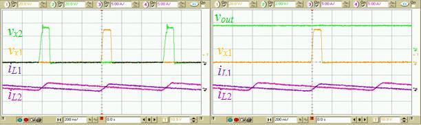
93 81 E.4 Convenional Inerleaved Buck Converer Figure E-7: Experimenal waveforms for he convenional inerleaved buck converer wih V in =48V & V ou =3.3V Figure E-8: Experimenal waveforms for he convenional inerleaved buck converer wih V in =48V & V ou =12V Figure E-9: Experimenal waveforms for he convenional inerleaved buck converer wih V in =24V & V ou =12V


94 82 Figure E-10: Experimenal waveforms for he convenional inerleaved buck converer wih V in =15V & V ou =12V v v x2 v i i v i i Figure E-11: Experimenal waveforms for he convenional inerleaved buck converer wih V in =6V & V ou =5V v x2 v i i v v i i Figure E-12: Experimenal waveforms for he convenional inerleaved buck converer wih V in =15V & V ou =3.3V
Investigation and Simulation Model Results of High Density Wireless Power Harvesting and Transfer Method
 Invesigaion and Simulaion Model Resuls of High Densiy Wireless Power Harvesing and Transfer Mehod Jaber A. Abu Qahouq, Senior Member, IEEE, and Zhigang Dang The Universiy of Alabama Deparmen of Elecrical
M2 3 Introduction to Switching Regulators. 1. What is a switching power supply? 2. What types of switchers are available?
 M2 3 Inroducion o Swiching Regulaors Objecive is o answerhe following quesions: 1. Wha is a swiching power supply? 2. Wha ypes of swichers are available? 3. Why is a swicher needed? 4. How does a swicher
Lecture 5: DC-DC Conversion
 1 / 31 Lecure 5: DC-DC Conversion ELEC-E845 Elecric Drives (5 ECTS) Mikko Rouimo (lecurer), Marko Hinkkanen (slides) Auumn 217 2 / 31 Learning Oucomes Afer his lecure and exercises you will be able o:
P. Bruschi: Project guidelines PSM Project guidelines.
 Projec guidelines. 1. Rules for he execuion of he projecs Projecs are opional. Their aim is o improve he sudens knowledge of he basic full-cusom design flow. The final score of he exam is no affeced by
Pulse Train Controlled PCCM Buck-Boost Converter Ming Qina, Fangfang Lib
 5h Inernaional Conference on Environmen, Maerials, Chemisry and Power Elecronics (EMCPE 016 Pulse Train Conrolled PCCM Buck-Boos Converer Ming Qina, Fangfang ib School of Elecrical Engineering, Zhengzhou
An Improved Zero-Voltage-Transition Technique in a Single-Phase Active Power Factor Correction Circuit
 An Improved Zero-lage-Transiion Technique in a Single-Phase Acive Power Facor Correcion Circui Suriya Kaewarsa School of Elecrical Engineering, Rajamangala Universiy of Technology Isan Sakon Nakhon Campus,
Table of Contents. 3.0 SMPS Topologies. For Further Research. 3.1 Basic Components. 3.2 Buck (Step Down) 3.3 Boost (Step Up) 3.4 Inverter (Buck/Boost)
 3.3 Boost (Step Up) 3.4 Inverter (Buck/Boost)") Table of Conens 3.0 SMPS Topologies 3.1 Basic Componens 3.2 Buck (Sep Down) 3.3 Boos (Sep Up) 3.4 nverer (Buck/Boos) 3.5 Flyback Converer 3.6 Curren Boosed Boos 3.7 Curren Boosed Buck 3.8 Forward Converer
Table of Conens 3.0 SMPS Topologies 3.1 Basic Componens 3.2 Buck (Sep Down) 3.3 Boos (Sep Up) 3.4 nverer (Buck/Boos) 3.5 Flyback Converer 3.6 Curren Boosed Boos 3.7 Curren Boosed Buck 3.8 Forward Converer
= f 8 f 2 L C. i C. 8 f C. Q1 open Q2 close (1+D)T DT 2. i C = i L. Figure 2: Typical Waveforms of a Step-Down Converter.
T DT 2. i C = i L. Figure 2: Typical Waveforms of a Step-Down Converter.") Inroducion Oupu Volage ipple in Sep-Down and Sep-Up Swiching egulaors Oupu volage ripple is always an imporan performance parameer wih DC-DC converers. For inducor-based swiching regulaors, several key
Inroducion Oupu Volage ipple in Sep-Down and Sep-Up Swiching egulaors Oupu volage ripple is always an imporan performance parameer wih DC-DC converers. For inducor-based swiching regulaors, several key
ISSCC 2007 / SESSION 29 / ANALOG AND POWER MANAGEMENT TECHNIQUES / 29.8
 ISSCC 27 / SESSION 29 / ANALOG AND POWER MANAGEMENT TECHNIQUES / 29.8 29.8 A 3GHz Swiching DC-DC Converer Using Clock- Tree Charge-Recycling in 9nm CMOS wih Inegraed Oupu Filer Mehdi Alimadadi, Samad Sheikhaei,
ORDER INFORMATION TO pin 320 ~ 340mV AMC7150DLF
 www.addmek.com DESCRIPTI is a PWM power ED driver IC. The driving curren from few milliamps up o 1.5A. I allows high brighness power ED operaing a high efficiency from 4Vdc o 40Vdc. Up o 200KHz exernal
Solid State Modulators for PIII Applications
 Solid Sae Modulaors for P Applicaions Dr. Marcel P.J. Gaudreau, P.E., Dr. Jeffrey A. Casey, Timohy J. Hawkey, Michael A. Kempkes, J. Michael Mulvaney; Diversified Technologies, nc. Absrac One of he key
Multiple Load-Source Integration in a Multilevel Modular Capacitor Clamped DC-DC Converter Featuring Fault Tolerant Capability
 Muliple Load-Source Inegraion in a Mulilevel Modular Capacior Clamped DC-DC Converer Feauring Faul Toleran Capabiliy Faisal H. Khan, Leon M. Tolber The Universiy of Tennessee Elecrical and Compuer Engineering
A New Voltage Sag and Swell Compensator Switched by Hysteresis Voltage Control Method
 Proceedings of he 8h WSEAS Inernaional Conference on ELECTRIC POWER SYSTEMS, HIGH VOLTAGES, ELECTRIC MACHINES (POWER '8) A New Volage Sag and Swell Compensaor Swiched by Hyseresis Volage Conrol Mehod AMIR
Family of Single-Inductor Multi-Output DC-DC Converters
 PEDS009 Family of Single-Inducor Muli-Oupu DC-DC Converers Ray-ee in Naional Cheng Kung Universiy No., a-hseuh Road ainan Ciy, aiwan rayleelin@ee.ncku.edu.w Chi-Rung Pan Naional Cheng Kung Universiy No.,
A Control Technique for 120Hz DC Output Ripple-Voltage Suppression Using BIFRED with a Small-Sized Energy Storage Capacitor
 90 Journal of Power Elecronics, Vol. 5, No. 3, July 005 JPE 5-3-3 A Conrol Technique for 0Hz DC Oupu Ripple-Volage Suppression Using BIFRED wih a Small-Sized Energy Sorage Capacior Jung-Bum Kim, Nam-Ju
University of Alberta
 Universiy of Albera Mulilevel Space Vecor PWM for Mulilevel Coupled Inducor Inverers by Behzad Vafakhah A hesis submied o he Faculy of Graduae Sudies and Research in parial fulfillmen of he requiremens
Proceedings of International Conference on Mechanical, Electrical and Medical Intelligent System 2017
 on Mechanical, Elecrical and Medical Inelligen Sysem 7 Consan On-ime Conrolled Four-phase Buck Converer via Saw-oohwave Circui and is Elemen Sensiiviy Yi Xiong a, Koyo Asaishi b, Nasuko Miki c, Yifei Sun
A1 K. 12V rms. 230V rms. 2 Full Wave Rectifier. Fig. 2.1: FWR with Transformer. Fig. 2.2: Transformer. Aim: To Design and setup a full wave rectifier.
 2 Full Wave Recifier Aim: To Design and seup a full wave recifier. Componens Required: Diode(1N4001)(4),Resisor 10k,Capacior 56uF,Breadboard,Power Supplies and CRO and ransformer 230V-12V RMS. + A1 K B1
Primary Side Control SMPS with Integrated MOSFET
 General Descripion GG64 is a primary side conrol SMPS wih an inegraed MOSFET. I feaures programmable cable drop compensaion and a peak curren compensaion funcion, PFM echnology, and a CV/CC conrol loop
BOUNCER CIRCUIT FOR A 120 MW/370 KV SOLID STATE MODULATOR
 BOUNCER CIRCUIT FOR A 120 MW/370 KV SOLID STATE MODULATOR D. Gerber, J. Biela Laboraory for High Power Elecronic Sysems ETH Zurich, Physiksrasse 3, CH-8092 Zurich, Swizerland Email: gerberdo@ehz.ch This
Three-Level TAIPEI Rectifier
 Three-Level TAIPEI Recifier Yungaek Jang, Milan M. Jovanović, and Juan M. Ruiz Power Elecronics Laboraory Dela Producs Corporaion 5101 Davis Drive, Research Triangle Park, C, USA Absrac A new low-cos,
EE 330 Lecture 24. Amplification with Transistor Circuits Small Signal Modelling
 EE 330 Lecure 24 Amplificaion wih Transisor Circuis Small Signal Modelling Review from las ime Area Comparison beween BJT and MOSFET BJT Area = 3600 l 2 n-channel MOSFET Area = 168 l 2 Area Raio = 21:1
GG6005. General Description. Features. Applications DIP-8A Primary Side Control SMPS with Integrated MOSFET
 General Descripion GG65 is a primary side conrol PSR SMPS wih an inegraed MOSFET. I feaures a programmable cable drop compensaion funcion, PFM echnology, and a CV/CC conrol loop wih high reliabiliy and
A ZVS Integrated Single-Input-Dual-Output DC/DC Converter for High Step-up Applications
 A ZS Inegraed Single-Inpu-Dual-Oupu / Converer for High Sep-up Applicaions Ming Shang, Suden Member, IEEE, Haoyu Wang, Member, IEEE School of Informaion Science and Technology ShanghaiTech Universiy Shanghai,
HF Transformer Based Grid-Connected Inverter Topology for Photovoltaic Systems
 1 HF Transformer Based Grid-Conneced Inverer Topology for Phoovolaic Sysems Abhiji Kulkarni and Vinod John Deparmen of Elecrical Engineering, IISc Bangalore, India. (abhijik@ee.iisc.erne.in, vjohn@ee.iisc.erne.in)
A Bidirectional Three-Phase Push-Pull Converter With Dual Asymmetrical PWM Method
 A Bidirecional Three-Phase Push-Pull Converer Wih Dual Asymmeral PWM Mehod Minho Kwon, Junsung Par, Sewan Choi, IEEE Senior Member Deparmen of Elecral and Informaion Engineering Seoul Naional Universiy
Phase-Shifting Control of Double Pulse in Harmonic Elimination Wei Peng1, a*, Junhong Zhang1, Jianxin gao1, b, Guangyi Li1, c
 Inernaional Symposium on Mechanical Engineering and Maerial Science (ISMEMS 016 Phase-Shifing Conrol of Double Pulse in Harmonic Eliminaion Wei Peng1, a*, Junhong Zhang1, Jianxin gao1, b, Guangyi i1, c
Chapter 1: Introduction
 Second ediion ober W. Erickson Dragan Maksimovic Universiy of Colorado, Boulder.. Inroducion o power processing.. Some applicaions of power elecronics.3. Elemens of power elecronics Summary of he course.
Linear PFC regulator for LED lighting with the multi-level structure and low voltage MOSFETs.
 Linear PFC regulaor for lighing wih he muli-level srucure and low volage MOSFETs. Yuichi Noge Nagaoka Universiy of Technology Niigaa, Japan noge@sn.nagaokau.ac.jp Jun-ichi Ioh Nagaoka Universiy of Technology
4 20mA Interface-IC AM462 for industrial µ-processor applications
 Because of he grea number of indusrial buses now available he majoriy of indusrial measuremen echnology applicaions sill calls for he sandard analog curren nework. The reason for his lies in he fac ha
Analysis ofthe Effects ofduty Cycle Constraints in Multiple-Input Converters for Photovoltaic Applications
 Analysis ofhe Effecs ofduy Cycle Consrains in Muliple-Inpu Converers for Phoovolaic Applicaions Junseok Song and Alexis Kwasinski Deparmen ofelecrical and Compuer Engineering The Universiy oftexas a Ausin
Automatic Power Factor Control Using Pic Microcontroller
 IDL - Inernaional Digial Library Of Available a:www.dbpublicaions.org 8 h Naional Conference on Advanced Techniques in Elecrical and Elecronics Engineering Inernaional e-journal For Technology And Research-2017
A Novel Bidirectional DC-DC Converter with Battery Protection
 Inernaional Journal of Engineering Research and Developmen e-issn: 2278-067X, p-issn : 2278-800X, www.ijerd.com Volume 5, Issue 1 (November 12), PP. 46-53 A Novel Bidirecional DC-DC Converer wih Baery
EE201 Circuit Theory I Fall
 EE1 Circui Theory I 17 Fall 1. Basic Conceps Chaper 1 of Nilsson - 3 Hrs. Inroducion, Curren and Volage, Power and Energy. Basic Laws Chaper &3 of Nilsson - 6 Hrs. Volage and Curren Sources, Ohm s Law,
Control and Protection Strategies for Matrix Converters. Control and Protection Strategies for Matrix Converters
 Conrol and Proecion Sraegies for Marix Converers Dr. Olaf Simon, Siemens AG, A&D SD E 6, Erlangen Manfred Bruckmann, Siemens AG, A&D SD E 6, Erlangen Conrol and Proecion Sraegies for Marix Converers To
EXPERIMENT #9 FIBER OPTIC COMMUNICATIONS LINK
 EXPERIMENT #9 FIBER OPTIC COMMUNICATIONS LINK INTRODUCTION: Much of daa communicaions is concerned wih sending digial informaion hrough sysems ha normally only pass analog signals. A elephone line is such
VOLTAGE DOUBLER BOOST RECTIFIER BASED ON THREE-STATE SWITCHING CELL FOR UPS APPLICATIONS
 VOLTAGE DOUBLER BOOST RECTIFIER BASED ON THREE-STATE SWITCHING CELL FOR UPS APPLICATIONS Raphael A. da Câmara, Ranoyca N. A. L. Silva, Gusavo A. L. Henn, Paulo P. Praça, Cícero M. T. Cruz, René P. Torrico-Bascopé
High Power Full-Bridge DC-DC Converter using a Center-Tapped Transformer and a Full-Wave Type Rectifier
 , pp.267-278 hp://dx.doi.org/10.14257/ijca.2014.7.4.23 High Power Full-Bridge DC-DC Converer using a Cener-Tapped Transformer and a Full-Wave Type Recifier Min-Gi Kim, Geun-Yong Park, Doo-HeeYoo and Gang-YoulJeong
Light-Load Efficiency Optimization Method
 Ligh-Load Efficiency Opimizaion Mehod Yungaek Jang, Milan M. Jovanović, and avid L. illman Power Elecronics Laboraory ela Producs Corporaion P.O. Box 273, 50 avis rive Research Triangle Park, NC 279 Absrac
PERFORMANCE OF DC TO DC DUAL ACTIVE BRIDGE CONVERTER DRIVING SINGLE PHASE INVERTER
 006-015 Asian Research Publishing Nework (ARPN). All righs reserved. PERFORMANCE OF DC TO DC DUAL ACTIVE BRIDGE CONVERTER DRIVING SINGLE PHASE INVERTER Digvijay B. Kanase, H. T. Jadhav and R. A. Meri Deparmen
ECMA st Edition / June Near Field Communication Wired Interface (NFC-WI)
") ECMA-373 1 s Ediion / June 2006 Near Field Communicaion Wired Inerface (NFC-WI) Sandard ECMA-373 1 s Ediion / June 2006 Near Field Communicaion Wired Inerface (NFC-WI) Ecma Inernaional Rue du Rhône 114
ECMA-373 1 s Ediion / June 2006 Near Field Communicaion Wired Inerface (NFC-WI) Sandard ECMA-373 1 s Ediion / June 2006 Near Field Communicaion Wired Inerface (NFC-WI) Ecma Inernaional Rue du Rhône 114
AN5028 Application note
 Applicaion noe Calculaion of urn-off power losses generaed by an ulrafas diode Inroducion This applicaion noe explains how o calculae urn-off power losses generaed by an ulrafas diode, by aking ino accoun
Bootstrap Gate Driver and Output Filter of An SC-based Multilevel Inverter for Aircraft APU
 Asian Power Elecronics Journal, Vol. 9, No. 2, Dec. 215 Boosrap Gae Driver and Oupu Filer o An C-based Mulilevel Inverer or Aircra APU Yuanmao YE,K.W.Eric CHENG, N.C. Cheung Power Elecronics Research Cenre,
An Integrated Three-port DC/DC Converter for High- Voltage Bus Based Photovoltaic Systems
 An Inegraed Three-por DC/DC Converer for High- Volage Bus Based Phoovolaic Sysems Junyun Deng, Suden Member, IEEE, Haoyu Wang, Member, IEEE, and Ming Shang School of Informaion Science and Technology ShanghaiTech
Communication Systems. Department of Electronics and Electrical Engineering
 COMM 704: Communicaion Lecure : Analog Mulipliers Dr Mohamed Abd El Ghany Dr. Mohamed Abd El Ghany, Mohamed.abdel-ghany@guc.edu.eg nroducion Nonlinear operaions on coninuous-valued analog signals are ofen
A New ZVS-PWM Full-Bridge Converter
 New ZV-PW Full-ridge onverer Yungaek Jang and ilan. Jovanović Dela Producs orporaion Power Elecronics Laboraory P.O. ox 73, 50 Davis Dr. Research Triangle Park, N 7709, U... Yu-ing hang DELT Elecronics
Explanation of Maximum Ratings and Characteristics for Thyristors
 8 Explanaion of Maximum Raings and Characerisics for Thyrisors Inroducion Daa shees for s and riacs give vial informaion regarding maximum raings and characerisics of hyrisors. If he maximum raings of
High-voltage high-frequency Marx-bank type pulse generator using integrated power semiconductor half-bridges
 High-volage high-frequency Marx-bank ype pulse generaor using inegraed power semiconducor half-bridges L.M. Redondo 1,2, J. Fernando Silva 1,3,4, P. Tavares 5, Elmano Margao 1,4 1 Insiuo Superior de Engenharia
Memorandum on Impulse Winding Tester
 Memorandum on Impulse Winding Teser. Esimaion of Inducance by Impulse Response When he volage response is observed afer connecing an elecric charge sored up in he capaciy C o he coil L (including he inside
Impacts of the dv/dt Rate on MOSFETs Outline:
 Ouline: A high dv/d beween he drain and source of he MOSFET may cause problems. This documen describes he cause of his phenomenon and is counermeasures. Table of Conens Ouline:... 1 Table of Conens...
Power Efficient Battery Charger by Using Constant Current/Constant Voltage Controller
 Circuis and Sysems, 01, 3, 180-186 hp://dx.doi.org/10.436/cs.01.304 Published Online April 01 (hp://www.scirp.org/journal/cs) Power Efficien Baery Charger by Using Consan Curren/Consan olage Conroller
Comparative Analysis of the Large and Small Signal Responses of "AC inductor" and "DC inductor" Based Chargers
 Comparaive Analysis of he arge and Small Signal Responses of "AC inducor" and "DC inducor" Based Chargers Ilya Zelser, Suden Member, IEEE and Sam Ben-Yaakov, Member, IEEE Absrac Two approaches of operaing
A New Isolated DC-DC Boost Converter using Three-State Switching Cell
 A New Isolaed DCDC Boos nverer using hreesae Swiching Cell René P. orricobascopé (1) Grover V. orricobascopé () Francisco A. A. de Souza (1) Carlos G. C. Branco (3) Cícero M.. Cruz (1) Luiz H. C. Barreo
ECMA-373. Near Field Communication Wired Interface (NFC-WI) 2 nd Edition / June Reference number ECMA-123:2009
 2 nd Edition / June Reference number ECMA-123:2009") ECMA-373 2 nd Ediion / June 2012 Near Field Communicaion Wired Inerface (NFC-WI) Reference number ECMA-123:2009 Ecma Inernaional 2009 COPYRIGHT PROTECTED DOCUMENT Ecma Inernaional 2012 Conens Page 1 Scope...
ECMA-373 2 nd Ediion / June 2012 Near Field Communicaion Wired Inerface (NFC-WI) Reference number ECMA-123:2009 Ecma Inernaional 2009 COPYRIGHT PROTECTED DOCUMENT Ecma Inernaional 2012 Conens Page 1 Scope...
4.5 Biasing in BJT Amplifier Circuits
 4/5/011 secion 4_5 Biasing in MOS Amplifier Circuis 1/ 4.5 Biasing in BJT Amplifier Circuis eading Assignmen: 8086 Now le s examine how we C bias MOSFETs amplifiers! f we don bias properly, disorion can
Three-Phase Isolated High-Power-Factor Rectifier Using Soft-Switched Two-Switch Forward Converter
 Three-Phase Isolaed High-Power-Facor Recifier Using Sof-Swiched Two-Swich Forward Converer Yungaek Jang, David L. Dillman, and Milan M. Jovanović Power Elecronics Laboraory Dela Producs Corporaion P.O.
Design And Implementation Of Multiple Output Switch Mode Power Supply
 Inernaional Journal of Engineering Trends and Technology (IJETT) Volume Issue 0-Oc 0 Design And Implemenaion Of Muliple Oupu Swich Mode Power Supply Ami, Dr. Manoj Kumar Suden of final year B.Tech. E.C.E.,
GaN-HEMT Dynamic ON-state Resistance characterisation and Modelling
 GaN-HEMT Dynamic ON-sae Resisance characerisaion and Modelling Ke Li, Paul Evans, Mark Johnson Power Elecronics, Machine and Conrol group Universiy of Noingham, UK Email: ke.li@noingham.ac.uk, paul.evans@noingham.ac.uk,
EXPERIMENT #4 AM MODULATOR AND POWER AMPLIFIER
 EXPERIMENT #4 AM MODULATOR AND POWER AMPLIFIER INTRODUCTION: Being able o ransmi a radio frequency carrier across space is of no use unless we can place informaion or inelligence upon i. This las ransmier
Development of Pulse Width Modulation LED drive
 ISSN 23069392, Inernaional Journal of Technology People Developing, Vol. 2, No. 3, DEC. 2012 Developmen of Pulse Widh Modulaion LED drive YuanPiao. Lee 1 ShihKuen. Changchien 2 ChainKuo Technology Universiy,
16.5 ADDITIONAL EXAMPLES
 16.5 ADDITIONAL EXAMPLES For reiew purposes, more examples of boh piecewise linear and incremenal analysis are gien in he following subsecions. No new maerial is presened, so readers who do no need addiional
Series-Resonant Converter with Reduced- Frequency-Range Control
 Series-Resonan Converer wih Reduced- Frequency-Range Conrol Yungaek Jang, Milan M. Jovanović, Juan M. Ruiz, and Gang Liu 1, Power Elecronics Laboraory, Dela Producs Corporaion, 511 Davis Drive, Research
Power losses in pulsed voltage source inverters/rectifiers with sinusoidal currents
 ree-wheeling diode Turn-off power dissipaion: off/d = f s * E off/d (v d, i LL, T j/d ) orward power dissipaion: fw/t = 1 T T 1 v () i () d Neglecing he load curren ripple will resul in: fw/d = i Lavg
DATA SHEET. 1N914; 1N916 High-speed diodes DISCRETE SEMICONDUCTORS Sep 03
 DISCRETE SEMICONDUCTORS DATA SHEET M3D176 Supersedes daa of April 1996 File under Discree Semiconducors, SC01 1996 Sep 03 FEATURES Hermeically sealed leaded glass SOD27 (DO-35) package High swiching speed:
Simulation Analysis of DC-DC Circuit Based on Simulink in Intelligent Vehicle Terminal
 Open Access Library Journal 218, Volume 5, e4682 ISSN Online: 2333-9721 ISSN Prin: 2333-975 Simulai Analysis of DC-DC Circui Based Simulink in Inelligen Vehicle erminal Weiran Li, Guoping Yang College
All Silicon Marx-bank topology for high-voltage, high-frequency rectangular pulses
 All Silicon Marx-bank opology for high-volage, high-frequency recangular pulses L.M. Redondo Cenro de Física da Universidade de Lisboa Insiuo Superior de Engenharia de Lisboa Rua Conselheiro Emídio Navarro
Implementation of High Voltage Gain RS Cell- Based DC-DC Converter for Offshore Wind
 IJCTA, 1(2), 217, pp. 147-156 Inernaional Science Press Closed Loop Conrol of Sof Swiched Forward Converer Using Inelligen Conroller 147 Implemenaion of High Volage Gain RS Cell- Based DC-DC Converer for
SCiCoreDrive62 +DC T5 U V W -DC. SCiCore 62. IGBT/MOSFET drivers
 PRELIMINARY TECHNICAL INFORMATION SCiCoreDrive62 IGBT/MOSFET drivers HIGHLIGHTS - 6 channel IGBT driver - suiable for 200V IGBT (900 V max on DCLink) - Up o 8 A peak oupu curren - Collecor sensing & faul
The Single-Stage TAIPEI Rectifier
 The Single-Sage TAIPEI Recifier Yungaek Jang, Milan M. Jovanović, and Juan M. Ruiz Power Elecronics Laboraory Dela Producs Corporaion 5101 Davis Drive, Research Triangle Park, C, USA Absrac A new hree-phase,
Reliability Improvement of FB inverter in HID Lamp Ballast using UniFET II MOSFET family
 Reliabiliy Improvemen of FB inverer in HID Lamp Ballas using UniFET II MOSFET family Won-Seok Kang Sysem & Applicaion Group Fairchild Semiconducor Bucheon, Korea wonseok.kang@fairchildsemi.com Jae-Eul
Design of a Three-Phase Unity Power Factor Single-Stage Telecom Rectifier
 Design of a Three-Phase Uniy Power Facor Single-Sage Telecom Recifier Bünyamin Tamyürek Deparmen of Elecrical Engineering, Eskisehir Osmangazi Universiy, Eskisehir, Turkey bamyurek@ogu.edu.r Absrac This
Analog Circuits EC / EE / IN. For
 Analog Circuis For EC / EE / IN By www.hegaeacademy.com Syllabus Syllabus for Analog Circuis Small Signal Equivalen Circuis of Diodes, BJTs, MOSFETs and Analog CMOS. Simple Diode Circuis, Clipping, Clamping,
A New, Two-Switch, Isolated, Three-Phase AC-DC Converter
 A ew, Two-Swich, Isolaed, Three-Phase AC-DC Converer Yungaek Jang, Milan M. Jovanovi, Misha Kumar, and Kuris High Power Elecronics Laboraory Dela Producs Corporaion Research Triangle Park, C, USA Yihua
A Coupled Inductor Hybrid Quadratic Boost Inverter for DC Microgrid Application
 A Coupled Inducor Hybrid Quadraic Boos Inverer for DC Microgrid Applicaion Anish Ahmad, R. K. Singh, and R. Mahany Deparmen of Elecrical Engineering, Indian Insiue of Technology (Banaras Hindu Universiy),Varanasi,India.
MODELING OF CROSS-REGULATION IN MULTIPLE-OUTPUT FLYBACK CONVERTERS
 MODELING OF CROSS-REGULATION IN MULTIPLE-OUTPUT FLYBACK CONVERTERS Dragan Maksimovićand Rober Erickson Colorado Power Elecronics Cener Deparmen of Elecrical and Compuer Engineering Universiy of Colorado,
AN303 APPLICATION NOTE
 AN303 APPLICATION NOTE LATCHING CURRENT INTRODUCTION An imporan problem concerning he uilizaion of componens such as hyrisors or riacs is he holding of he componen in he conducing sae afer he rigger curren
A New Three-Phase Two-Switch ZVS PFC DCM Boost Rectifier
 A New Three-Phase Two-Swich ZVS PFC DCM Boos Recifier Yungaek Jang, Milan M. Jovanović, and Juan M. Ruiz Power Elecronics Laboraory Dela Producs Corporaion 5101 Davis Drive, Research Triangle Park, NC,
Development of Temporary Ground Wire Detection Device
 Inernaional Journal of Smar Grid and Clean Energy Developmen of Temporary Ground Wire Deecion Device Jing Jiang* and Tao Yu a Elecric Power College, Souh China Universiy of Technology, Guangzhou 5164,
Aleksandrs Andreiciks, Riga Technical University, Ingars Steiks, Riga Technical University, Oskars Krievs, Riga Technical University
 Scienific Journal of Riga Technical Universiy Power and Elecrical Engineering Curren-fed Sep-up DC/DC Converer for Fuel Cell Applicaions wih Acive Overvolage Clamping Aleksandrs Andreiciks, Riga Technical
4D-Interleaving of Isolated ISOP Multi-Cell Converter Systems for Single Phase AC/DC Conversion
 2016 IEEE Proceedings of he Conference for Power Elecronics, Inelligen Moion, Power Qualiy (PCIM Europe 2016), Nuremberg, Germany, May 10-12, 2016 4D-Inerleaving of Isolaed ISOP Muli-Cell Converer Sysems
Three-Level TAIPEI Rectifier Analysis of Operation, Design Considerations, and Performance Evaluation
 This aricle has been acceped for publicaion in a fuure issue of his journal, bu has no been fully edied. Conen may change prior o final publicaion. Ciaion informaion: DOI.9/TPEL.6.5437, IEEE Transacions
Design and Development of Zero Voltage Switched Full Bridge 5 kw DC Power Supply
 Inernaional Journal of Engineering Research & Technology (IJERT) Design and Developmen of Zero Volage Swiched Full Bridge 5 kw DC Power Supply ISSN: 2278-181 Vol. 3 Issue 5, May - 214 S. K. Agrawal, S.
PRM and VTM Parallel Array Operation
 APPLICATION NOTE AN:002 M and V Parallel Array Operaion Joe Aguilar VI Chip Applicaions Engineering Conens Page Inroducion 1 High-Level Guidelines 1 Sizing he Resisor 4 Arrays of Six or More Ms 5 Sysem
Application Note 5324
 Desauraion Faul Deecion Opocoupler Gae Drive Producs wih Feaure: PLJ, PL0J, PLJ, PL1J and HCPLJ Applicaion Noe 1. Inroducion A desauraion faul deecion circui provides proecion for power semiconducor swiches
f t 2cos 2 Modulator Figure 21: DSB-SC modulation.
 4.5 Ampliude modulaion: AM 4.55. DSB-SC ampliude modulaion (which is summarized in Figure 21) is easy o undersand and analyze in boh ime and frequency domains. However, analyical simpliciy is no always
Installation and Operating Instructions for ROBA -brake-checker Typ
 (B.018102.EN) Guidelines on he Declaraion of Conformiy A conformiy evaluaion has been carried ou for he produc in erms of he EC Low Volage Direcive 2006/95/ EC and EMC Direcive 2004/108/EC. The Declaraion
Introduction to Power Electronics ECEN 4797/5797
 Lecure 1: Augus 27, 2012 Inroducion o Power Elecronics ECEN 4797/5797 Rober W. Erickson Universiy of Colorado, Boulder Fall 2012 1 Inroducion o Power Elecronics ECEN 4797/5797 Insrucor: Prof. Bob Erickson
MX6895BETR. -550V Full Bridge Gate Driver INTEGRATED CIRCUITS DIVISION. Features. Description. Applications. Ordering Information
 -550V Full Bridge Gae Driver INTEGRATED CIRCUITS DIVISION Feaures Full Bridge Gae Driver Inernal High Volage Level Shif Funcion Negaive 550V Lamp Supply Volage 3V o 12V CMOS Logic Compaible 8V o 12V Inpu
Analysis of SiC MOSFETs under Hard and Soft- Switching
 Analysis of SiC MOSFETs under Hard and Sof- Swiching M. R. Ahmed, R. Todd and A. J. Forsyh School of Elecrical and Elecronic Engineering, Power Conversion Group The Universiy of Mancheser Mancheser, U.K.
CURRENT MODE PWM+PFM CONTROLLER WITH BUILT-IN HIGH VOLTAGE MOSFET
 CURRENT MODE PWM+PFM CONTROLLER WITH BUILT-IN HIGH VOLTAGE MOSFET DESCRIPTION SD6835 is curren mode PWM+PFM conroller used for SMPS wih buil-in high-volage MOSFET and exernal sense resisor. I feaures low
Variation Aware Cross-Talk Aggressor Alignment by Mixed Integer Linear Programming
 ariaion Aware Cross-alk Aggressor Alignmen by Mixed Ineger Linear Programming ladimir Zoloov IBM. J. Wason Research Cener, Yorkown Heighs, NY zoloov@us.ibm.com Peer Feldmann D. E. Shaw Research, New York,
Application Note AN-1083
 Applicaion Noe AN-1083 Feaures of he Low-Side Family IPS10xx By Fabio Necco, Inernaional Recifier Table of Conens Page Inroducion...1 Diagnosis...1 Inpu Curren vs. Temperaure...1 Selecion of he Resisor
EE 40 Final Project Basic Circuit
 EE 0 Spring 2006 Final Projec EE 0 Final Projec Basic Circui Par I: General insrucion 1. The final projec will coun 0% of he lab grading, since i s going o ake lab sessions. All oher individual labs will
7 th International Conference on DEVELOPMENT AND APPLICATION SYSTEMS S u c e a v a, R o m a n i a, M a y 27 29,
 7 h Inernaional Conference on DEVEOPMENT AND APPICATION SYSTEMS S u c e a v a, o m a n i a, M a y 27 29, 2 0 0 4 THEE-PHASE AC CHOPPE WITH IGBT s Ovidiu USAU 1, Mihai UCANU, Crisian AGHION, iviu TIGAEU
Self-Precharge in Single-Leg Flying Capacitor Converters
 Self-Precharge in Single-Leg Flying Capacior Converers Seven Thielemans Elecrical Energy, Sysems and Auomaion Deparmen Ghen Universiy (UGen), EESA Ghen, Belgium Email: Seven.Thielemans@UGen.be Alex uderman
International Journal of Electronics and Electrical Engineering Vol. 4, No. 2, April Supercapacitors
 Inernaional Journal of Elecronics and Elecrical Engineering Vol. 4, No., April 16 Equalizaion Chargers Using Parallel- or SeriesParallel-Resonan Inverer for Series-Conneced Supercapaciors Yifan Zhou and
Research Article Comparison between Phase-Shift Full-Bridge Converters with Noncoupled and Coupled Current-Doubler Rectifier
 The Scienific World Journal Volume 013, ricle I 61896, 11 pages hp://dx.doi.org/10.1155/013/61896 esearch ricle omparison beween Phase-Shif Full-ridge onverers wih Noncoupled and oupled urren-oubler ecifier
Comparative Study of Feed Forward and SPWM Control Technique for DC to DC Dual Active Bridge Converter Driving Single Phase Inverter
 JRST nernaional Journal for nnovaive Research in Science & Technology Volume 3 ssue 1 June 216 SSN (online): 2349-61 Comparaive Sudy of Feed Forward and SPWM Conrol Technique for DC o DC Dual Acive Bridge
Study on the Wide Gap Dielectric Barrier Discharge Device Gaofeng Wang
 Sudy on he Wide Gap Dielecric Barrier Discharge Device Gaofeng Wang School of Informaion Engineering, Zhengzhou Universiy, Zhengzhou 450001, China 932167312@qq.com Keywords: DBD; Wide air gap; Plasma body;
<Diode Modules> RM200CY-24S HIGH POWER SWITCHING USE INSULATED TYPE
 dual swich (Cahode Common) Forward curren...... 2 0 0 A Repeiive peak reverse volage V RRM... 1 2 0 0 V Maximum juncion emperaure T jmax... 1 5 0 C Fla base Type Copper base plae RoHS Direcive