a leap ahead in analog
|
|
|
- Ross Doyle
- 6 years ago
- Views:
Transcription

1 Analog modeling requirements for HV CMOS technology Ehrenfried Seebacher a leap ahead in analog
2 Presentation Overview Design perspective on High Performance Analog HV CMOS Analog modeling requirements HV Transistor compact modeling Aging modeling 1/f noise modeling Process Variability 2
3 Design Perspective on Analog Modeling Analog Application Critical feature Critical Modeling Parameter Pre-Amplifier for ADC Reference circuit 3 Signal to noise ratio, effective number of Bits Transistor and resistor noise ADC/DAC Linearity,Distortion Resistor Mismatch Operational Amplifier Current Mirror Multi-channel devices Voltage Reference (e.g. Bandgap) Current Reference Voltage matching Current matching Gain matching Voltage stability Current stability Analog parameter (gds, gm, Vt etc.) mismatch Bipolar parasitics (gain, linearity etc.)
4 Design Perspective on Analog Modeling Analog Application Critical feature Critical Modeling Parameter Capacitor switching design Transmission gates IC/RC Oscillator High impedance signal source Current source Operational Amplifier Operational Amplifier Voltage Reference parasitic voltage divider Charge Injection frequency stability capacitive coupling Output resistance Gain Offset & Gain shift Output voltage shift Parasitic capacitance Small signal parameters (gds, gm etc.) 2nd order parameters (linearity and temperature) 4
5 HV TRANSISTOR MODELING 5
6 FOMs for HV Transistors RON (On Resistor) (high vgs, low vds, and temp.) IDSAT (Saturation Current)? VT long & short Cgg & Cgd Miller Cap? Analog parameter for long channel length (gds, gm) RF Parameter FT, FMAX? 1/f noise. 6
7 State of the Art HV Compact Models and new Developments EKV HV Transistor Under development within the EU Project COMON A Physics-Based Analytical Compact Model for the Drift Region of the HV-MOSFET Antonios Bazigos, François Krummenacher, Jean-Michel Sallese, Matthias Bucher, Ehrenfried Seebacher, Werner Posch, Kund Molnár, and Mingchun Tang HiSIM_HV CMC Standard model version ;1.2.1; 2.0 PSP HV Transistor Model In development based on PSP surface potential model MM20 asymmetrical, surface-potential-based LDMOS model, developed by NXP Research BSIMx Sub-circuit Model 7
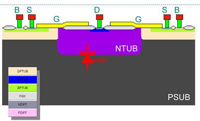
8 HV CMOS Transistor Types PWELL Increased junction breakdown voltage (BV) of the drain diffusion is achieved by using a deep drain well Small on-resistance and high BV are contrary effects. The optimization of the tradeoff between both quantities is of major interest. The gate length is extended beyond the body-drain well junction, which increases the junction BV. The gate acts as a field plate to bends the electric field. RESURFeffect Quasisaturation Effect. PWELL NWELL Nwell Nwell 8
9 Sub-circuit Modeling 9
10 HiSIM_HV Complete Surface potential-based: HiSIM_HV solves the Poisson equation along the MOSFET channel iteratively, including the resistance effect in the drift region. high flexibility 20 model flags scales with the gate width, the gate length, the number of gate fingers and the drift region length. In addition, HiSIM_HV is capable of modeling symmetric and asymmetric HV devices. The following effects are also included: Depletion effect of the gate polycrystalline silicon (poly-si). Quantum mechanical CLM Narrow channel STI Leakage currents (gate, substrate and gate-induced drain leakage (GIDL) currents). Source/bulk and drain/bulk diode models. Noise models (1/f, thermal noise, induced gate noise). Non-quasi static (NQS) model. 10
11 Model Benchmark Output Characteristic 11
12 AC Modeling: Cgg BSIM3+JFETS Subckt. HiSIM_HV Subcircuit: bad fitting quality, especially in accumulation. HiSIM_HV: good fitting quality in all regions. 12
13 Short Device: Transfer Characteristics at low and high Vds x: Meas. Blue: Green: Red: EPFL_HV BSIM subcircuit HISIM_HV

14 Short Device: Output Characteristics x: Measurement Blue: EPFL_HV Green: BSIM sub-circuit Red: HISIM_HV
15 Table of Model Capabilities (1/3) Physical Effects BSIM3/JFET Subcircuit HiSIM_HV EPFL-HV Technology Related Device Effects: Symmetric / Asymmetric Device asymmetric only Quasi-Saturation RON Mobility Carrier Velocity Saturation Channel Length Modulation Impact Ionization current extrinsic model Poly-Silicon-Gate Depletion Effects Geometry Scaling: Short Channel Effects Reverse Short Channel Effects Narrow Channel Effects Drain Induced Barrier Lowering
16 Table of Model Capabilities (2/3) Physical Effects BSIM3/JFET Subcircuit HiSIM_HV EPFL-HV Asymetric MOS Capacitances: Intrinsic Capacitance Overlap Capacitance Fringing Capacitance Bulk Diodes: Diode Current Diode Capacitance Temperature Modelling: Threshold Voltage Mobility Quasi-Saturation RON Bulk Current Self-Heating
17 Table of Model Capabilities (3/3) Physical Effects BSIM3/JFET Subcircuit HiSIM_HV EPFL-HV Noise: SPICE Noise model Flicker Noise Model Short Channel Thermal Noise Model Induced Noise in Gate Induced Noise in Substrate RF Modeling: Gate resistance model Substrate resistance model Multi-finger transistors Non-Quasi-Static (NQS): NQS
18 Modeling of parasitic diodes and bipolar in HV transistors PARASITIC MODELING 18
19 Benchmarking HiSIM_HV for 120V Transistors HV NMOS output and transfer characteristic of a typical wafer. W/L=40/0.5, VGS= 2.9, 4.8, 6.7, 8.6, 10.5, 12.4, 14.3, 16.2, 18.1, 20 V, VBS=0 V. & VBS= 0, -1, -2, -3, -4 V, VDS=0.1 V. + = measured, full lines= BSIM3v3 model; dashed lines = HiSIM_HV
20 Isolated HVMOS: High-Side Switch Modeling - HVMOS used on the low-side of a load: Transfer Characteristics Source and Substrate hold at the same potential - HVMOS used on the high-side of a load: Both Source and Drain can be placed at high potential => Ron is changing with V sub-s Vd=0.1V, Vs=Vb=0 HiSIM_HV 1.2.1: Vsub modulates the effective depth of the drift region: Rdrift(V sub,s ) Vsub=0 Vsub=-120V 20
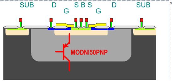
21 HV Transistor Parasitic Modeling 21
22 Analog design requirement 1/F NOISE MODELING 22
23 1/f Noise Modeling for HV Transistors 23 Mobility fluctuations as well as charge carrier fluctuations HiSIM_HV: NFALP which is applied for the mobility fluctuation phenomenon NFTRP which is applied for the ratio of trapped density to attenuation coefficient. CIT, a capacitance parameter applied for interface-trapped carriers. Normally it is fixed to zero. 1.) The BSIM3v3 approach has a different formulation for operating regions vg > vth + 0.1V and vg < vth + 0.1V; Therefore a discontinuous flicker noise model may occur HiSIM_HV which uses one common formulation for strong and weak inversion operating regions. 2.) The DC modeling approach is of course different therefore the thermal noise description will also differ. 3.) Another approach to check is the input referred noise. For accurate gm modeling also the input referred noise is simulated with higher accuracy. If the gm does not differ much from both HV model approaches then the noise models it can be compared
 measurements: black crosses, HiSIM_HV: red lines, BSIM3v3: dark")
24 Sid & Svg Benchmark Sid Output referred Noise & Svg input referred Noise Vds=3V versus inversion coefficient IC for a short channel and a long channel device (lower curves) measurements: black crosses, HiSIM_HV: red lines, BSIM3v3: dark lines 24
25 HV transistor performance constraints between RON and lifetime AGING MODELING 25
26 Transistor Aging Effects and Reliability Constraints Hot Carrier induced stress (HCS) for analog operation: Transistors are stressed at VDSmax and VGS=Vt+Voverdrive. Vt, IDSAT, IDlin and GMmax are used as degradation parameters. The maximum allowed shift e.g. 10% for analog applications within extrapolated target lifetime (10 years with Duty Factor of 100). Biased temperature high gate stress (BTS-VGS): PMOS transistors are stressed at high temperature (e.g. T=125 C) and maximum Gate voltage. The shift in threshold voltage (BMi) is used as degradation parameter for this effect. The maximum allowed shift e.g. 10% for analog applications within extrapolated target lifetime (10 years with Duty Factor of 100). 26
 RD=f(t) = Aging Simulator n At P=f(t) Sum (p.")
27 Aging Simulation SPICE Input dec & Schematic Analog Simulator Analog Simulator + Aging Parameter Model VT=f(t) RD=f(t) = Aging Simulator n At P=f(t) Sum (p.t) Extrapolate product lifetime 27
28 Aging Modeling HC: The de facto modeling method to analyze CHC is based on substrate current Isub, NBTI: Generation of interface traps at Si/SiO2 interface Vt degradation partial recovery HC and NBTI Modeling with Reaction Diffusion and hole trapping/detrapping mechanism : VT, U0, RON = f (N it ) =f (isub, ids) R D mechanism. (a) NBTI: 1-D hydrogen species diffusion. (b) CHC: 2-D hot-carrier trapping. Compact Modeling and Simulation of Circuit Reliability for 65-nm CMOS Technology: Wenping Wang IEEE TRANSACTIONS ON DEVICE AND MATERIALS RELIABILITY, VOL. 7, NO. 4, DECEMBER
29 HC Stress 4.7V IDsat 150s [%] IDsat shift % Operating point definition: VD=VDmax, VG=VGmax 3 2,5 2 1,5 1 0,5 0 5,00E-03 5,20E-03 5,40E-03 5,60E-03 5,80E-03 6,00E-03 6,20E-03 t0 [A] Idlin 150s [%] IDlin shift % Operating point definition: VD=0.1V, VG=VGmax 1,50E-04 1,60E-04 1,70E-04 1,80E-04 1,90E-04 2,00E-04 2,10E-04 2,20E-04 2,30E-04 t0 [A] 29
30 WC Reliability Model Investigation: WC models v. reliability effects Consideration of output characterisitc shows: Saturation region ID variation covered also for stressed device Linear region Change in the resistive behavior abs value of ID below WC emphasis Additional reliability modeling necessary WC Model fail 30
31 WC Reliability Model Result: Perfect curve fit due to the included PV method Triode region shows also perfect fit after introduction of series resistance Length dependency taken into account by voltage divider behavior This method is reliable provides fast simulation opportunity d Introduced Sub-circuit RD New Aging WC Model Set Including PV and HC g b s 32
32 High Performance Analog Variability of analog parameter gm/id; gds; 1/f noise Mismatch of active and passive devices PROCESS VARIABILITY 33


33 1/f Noise Process Variability 1/f noise variability Variability increase with smaller ID Variability increase with smaller L Lorentzian Noise Covered with WC models 34
34 GDS MAP Implementation (1430 Data) v. WC Model NMOS VGS=0.8V PMOS VGS=0.9V NMOS VTH + 250mV PMOS VTH + 250mV 35
35 H18 GDS BSIM3v3 W/L= 10/2.0 (alpha3 version) Standard Gds Modeling VGS= V Analog Gds Modeling NFET PFET VGS=-0.47V Gds Modeling 36
36 GDS with PSP and HiSIM2 PSP Standard Gds Modeling W/L=10/2 NFET PFET HiSIM2 W/L=10/1.2 37
37 Summary Analog modeling requirements for HV CMOS technology: Analog design relies on Careful modeling of HV transistor Additionally PV for Small signal parameter, parasitic modeling, 1/f noise Need for aging modelling 38
Contents. Contents... v. Preface... xiii. Chapter 1 Introduction...1. Chapter 2 Significant Physical Effects In Modern MOSFETs...
 Contents Contents... v Preface... xiii Chapter 1 Introduction...1 1.1 Compact MOSFET Modeling for Circuit Simulation...1 1.2 The Trends of Compact MOSFET Modeling...5 1.2.1 Modeling new physical effects...5
Analog performance of advanced CMOS and EKV3 model
 NanoTera Workshop on Next-Generation MOSFET Compact Models EPFL, December 15-16, 2011 Analog performance of advanced CMOS and EKV3 model Matthias Bucher Assistant Professor Technical University of Crete
1286 IEEE TRANSACTIONS ON ELECTRON DEVICES, VOL. 52, NO. 7, JULY MOSFET Modeling for RF IC Design
 1286 IEEE TRANSACTIONS ON ELECTRON DEVICES, VOL. 52, NO. 7, JULY 2005 MOSFET Modeling for RF IC Design Yuhua Cheng, Senior Member, IEEE, M. Jamal Deen, Fellow, IEEE, and Chih-Hung Chen, Member, IEEE Invited
Gennady Gildenblat. Editor. Compact Modeling. Principles, Techniques and Applications. Springer
 Gennady Gildenblat Editor Compact Modeling Principles, Techniques and Applications Springer Contents Part I Compact Models of MOS Transistors 1 Surface-Potential-Based Compact Model of Bulk MOSFET 3 Gennady
Fundamentals of Power Semiconductor Devices
 В. Jayant Baliga Fundamentals of Power Semiconductor Devices 4y Spri ringer Contents Preface vii Chapter 1 Introduction 1 1.1 Ideal and Typical Power Switching Waveforms 3 1.2 Ideal and Typical Power Device
Lecture-45. MOS Field-Effect-Transistors Threshold voltage
 Lecture-45 MOS Field-Effect-Transistors 7.4. Threshold voltage In this section we summarize the calculation of the threshold voltage and discuss the dependence of the threshold voltage on the bias applied
Sub-Threshold Region Behavior of Long Channel MOSFET
 Sub-threshold Region - So far, we have discussed the MOSFET behavior in linear region and saturation region - Sub-threshold region is refer to region where Vt is less than Vt - Sub-threshold region reflects
COMON De-Briefing. Prof. Benjamin Iñiguez
 COMON De-Briefing Prof. Benjamin Iñiguez Department of Electronic, Electrical and Automatic Control Engineering, Universitat Rovira i Virgili (URV) Tarragona, Spain benjamin.iniguez@urv.cat MOS-AK, Munich,
FUNDAMENTALS OF MODERN VLSI DEVICES
 19-13- FUNDAMENTALS OF MODERN VLSI DEVICES YUAN TAUR TAK H. MING CAMBRIDGE UNIVERSITY PRESS Physical Constants and Unit Conversions List of Symbols Preface page xi xiii xxi 1 INTRODUCTION I 1.1 Evolution
ECE520 VLSI Design. Lecture 2: Basic MOS Physics. Payman Zarkesh-Ha
 ECE520 VLSI Design Lecture 2: Basic MOS Physics Payman Zarkesh-Ha Office: ECE Bldg. 230B Office hours: Wednesday 2:00-3:00PM or by appointment E-mail: pzarkesh@unm.edu Slide: 1 Review of Last Lecture Semiconductor
Tradeoffs and Optimization in Analog CMOS Design
 Tradeoffs and Optimization in Analog CMOS Design David M. Binkley University of North Carolina at Charlotte, USA A John Wiley & Sons, Ltd., Publication Contents Foreword Preface Acknowledgmerits List of
UNIT 3: FIELD EFFECT TRANSISTORS
 FIELD EFFECT TRANSISTOR: UNIT 3: FIELD EFFECT TRANSISTORS The field effect transistor is a semiconductor device, which depends for its operation on the control of current by an electric field. There are
Accuracy and Speed Performance of HiSIM Versions 231 and 240
 Accuracy and Speed Performance of HiSIM Versions 231 and 240 H.J. Mattausch, M. Miura-Mattausch, N. Sadachika, M. Miyake Graduate School of Advanced Sciences of Matter, Hiroshima University T. Iizuka NEC
Lecture 16: MOS Transistor models: Linear models, SPICE models. Context. In the last lecture, we discussed the MOS transistor, and
 Lecture 16: MOS Transistor models: Linear models, SPICE models Context In the last lecture, we discussed the MOS transistor, and added a correction due to the changing depletion region, called the body
Field-Effect Transistor (FET) is one of the two major transistors; FET derives its name from its working mechanism;
 is one of the two major transistors; FET derives its name from its working mechanism;") Chapter 3 Field-Effect Transistors (FETs) 3.1 Introduction Field-Effect Transistor (FET) is one of the two major transistors; FET derives its name from its working mechanism; The concept has been known
Chapter 3 Field-Effect Transistors (FETs) 3.1 Introduction Field-Effect Transistor (FET) is one of the two major transistors; FET derives its name from its working mechanism; The concept has been known
Solid State Devices- Part- II. Module- IV
 Solid State Devices- Part- II Module- IV MOS Capacitor Two terminal MOS device MOS = Metal- Oxide- Semiconductor MOS capacitor - the heart of the MOSFET The MOS capacitor is used to induce charge at the
EE70 - Intro. Electronics
 EE70 - Intro. Electronics Course website: ~/classes/ee70/fall05 Today s class agenda (November 28, 2005) review Serial/parallel resonant circuits Diode Field Effect Transistor (FET) f 0 = Qs = Qs = 1 2π
Conduction Characteristics of MOS Transistors (for fixed Vds)! Topic 2. Basic MOS theory & SPICE simulation. MOS Transistor
! Topic 2. Basic MOS theory & SPICE simulation. MOS Transistor") Conduction Characteristics of MOS Transistors (for fixed Vds)! Topic 2 Basic MOS theory & SPICE simulation Peter Cheung Department of Electrical & Electronic Engineering Imperial College London (Weste&Harris,
Conduction Characteristics of MOS Transistors (for fixed Vds)! Topic 2 Basic MOS theory & SPICE simulation Peter Cheung Department of Electrical & Electronic Engineering Imperial College London (Weste&Harris,
Topic 2. Basic MOS theory & SPICE simulation
 Topic 2 Basic MOS theory & SPICE simulation Peter Cheung Department of Electrical & Electronic Engineering Imperial College London (Weste&Harris, Ch 2 & 5.1-5.3 Rabaey, Ch 3) URL: www.ee.ic.ac.uk/pcheung/
Conduction Characteristics of MOS Transistors (for fixed Vds) Topic 2. Basic MOS theory & SPICE simulation. MOS Transistor
 Topic 2. Basic MOS theory & SPICE simulation. MOS Transistor") Conduction Characteristics of MOS Transistors (for fixed Vds) Topic 2 Basic MOS theory & SPICE simulation Peter Cheung Department of Electrical & Electronic Engineering Imperial College London (Weste&Harris,
Conduction Characteristics of MOS Transistors (for fixed Vds) Topic 2 Basic MOS theory & SPICE simulation Peter Cheung Department of Electrical & Electronic Engineering Imperial College London (Weste&Harris,
Modeling Snapback and Rise-Time Effects in TLP Testing for ESD MOS Devices Using BSIM3 and VBIC Models
 Modeling Snapback and Rise-Time Effects in TLP Testing for ESD MOS Devices Using BSIM3 and VBIC Models, Duane Connerney, Ronald Carroll, Timwah Luk Fairchild Semiconductor, South Portland, ME 04106 1 Outline
Georgia Institute of Technology School of Electrical and Computer Engineering. Midterm Exam
 Georgia Institute of Technology School of Electrical and Computer Engineering Midterm Exam ECE-3400 Fall 2013 Tue, September 24, 2013 Duration: 80min First name Solutions Last name Solutions ID number
PSP model update. Gert-Jan Smit, Andries Scholten, D.B.M. Klaassen (NXP Semiconductors) Ramses van der Toorn (Delft University of Technology)
 Ramses van der Toorn (Delft University of Technology)") PSP model update Gert-Jan Smit, Andries Scholten, D.B.M. Klaassen (NXP Semiconductors) Ramses van der Toorn (Delft University of Technology) MOS-AK, San Francisco 12 December 2012 outline some history
PSP model update Gert-Jan Smit, Andries Scholten, D.B.M. Klaassen (NXP Semiconductors) Ramses van der Toorn (Delft University of Technology) MOS-AK, San Francisco 12 December 2012 outline some history
Compact Modelling of HVMOSFETs
 MOS- AK Mee;ng, Technical University of Munich Munich, April 11-12, 2013 Compact Modelling of HVMOSFETs MaKhias Bucher 12, Nikos Mavredakis 1 Antonios Bazigos 2, François Krummenacher 2, Jean- Michel Sallese
How is a CMC Standard Model Implemented And Verified in a Simulator?
 How is a CMC Standard Model Implemented And Verified in a Simulator? MOS-AK Workshop, Jushan Xie Vice Chairman of the CMC Senior Architect, Cadence Design Systems, Inc. 1 Content Benefit of CMC standard
EE301 Electronics I , Fall
 EE301 Electronics I 2018-2019, Fall 1. Introduction to Microelectronics (1 Week/3 Hrs.) Introduction, Historical Background, Basic Consepts 2. Rewiev of Semiconductors (1 Week/3 Hrs.) Semiconductor materials
NAME: Last First Signature
 UNIVERSITY OF CALIFORNIA, BERKELEY College of Engineering Department of Electrical Engineering and Computer Sciences EE 130: IC Devices Spring 2003 FINAL EXAMINATION NAME: Last First Signature STUDENT
8. Characteristics of Field Effect Transistor (MOSFET)
") 1 8. Characteristics of Field Effect Transistor (MOSFET) 8.1. Objectives The purpose of this experiment is to measure input and output characteristics of n-channel and p- channel field effect transistors
1 8. Characteristics of Field Effect Transistor (MOSFET) 8.1. Objectives The purpose of this experiment is to measure input and output characteristics of n-channel and p- channel field effect transistors
MOSFET short channel effects
 MOSFET short channel effects overview Five different short channel effects can be distinguished: velocity saturation drain induced barrier lowering (DIBL) impact ionization surface scattering hot electrons
Compact Modeling of Silicon Carbide Lateral FETs for High Temperature Analog and Digital Circuits
 Compact Modeling of Silicon Carbide Lateral FETs for High Temperature Analog and Digital Circuits Avinash S. Kashyap Cheng-Po Chen Vinayak Tilak GE Global Research Center 12/7/2011 Overview Program Objectives:
MEASUREMENT AND INSTRUMENTATION STUDY NOTES UNIT-I
 MEASUREMENT AND INSTRUMENTATION STUDY NOTES The MOSFET The MOSFET Metal Oxide FET UNIT-I As well as the Junction Field Effect Transistor (JFET), there is another type of Field Effect Transistor available
UNIVERSITY OF CALIFORNIA AT BERKELEY College of Engineering Department of Electrical Engineering and Computer Sciences.
 UNIVERSITY OF CALIFORNIA AT BERKELEY College of Engineering Department of Electrical Engineering and Computer Sciences Discussion #9 EE 05 Spring 2008 Prof. u MOSFETs The standard MOSFET structure is shown
INTERNATIONAL JOURNAL OF APPLIED ENGINEERING RESEARCH, DINDIGUL Volume 1, No 3, 2010
 Low Power CMOS Inverter design at different Technologies Vijay Kumar Sharma 1, Surender Soni 2 1 Department of Electronics & Communication, College of Engineering, Teerthanker Mahaveer University, Moradabad
Semiconductor Physics and Devices
 Metal-Semiconductor and Semiconductor Heterojunctions The Metal-Oxide-Semiconductor Field-Effect Transistor (MOSFET) is one of two major types of transistors. The MOSFET is used in digital circuit, because
UNIT-1 Bipolar Junction Transistors. Text Book:, Microelectronic Circuits 6 ed., by Sedra and Smith, Oxford Press
 UNIT-1 Bipolar Junction Transistors Text Book:, Microelectronic Circuits 6 ed., by Sedra and Smith, Oxford Press Figure 6.1 A simplified structure of the npn transistor. Microelectronic Circuits, Sixth
444 Index. F Fermi potential, 146 FGMOS transistor, 20 23, 57, 83, 84, 98, 205, 208, 213, 215, 216, 241, 242, 251, 280, 311, 318, 332, 354, 407
 Index A Accuracy active resistor structures, 46, 323, 328, 329, 341, 344, 360 computational circuits, 171 differential amplifiers, 30, 31 exponential circuits, 285, 291, 292 multifunctional structures,
TSMC Property. The Impacts of BSIM. Sally Liu TSMC. S. Liu TSMC, Ltd Dec 13, 2012P TSMC, Ltd
 The Impacts of BSIM Sally Liu TSMC 1 The Impacts of BSIM Outline What is BSIM Industry standard Breadth and depth Moving forward 2 What s in a name of BSIM The making of BSIM 631 papers in IEEE Explore
EE241 - Spring 2013 Advanced Digital Integrated Circuits. Projects. Groups of 3 Proposals in two weeks (2/20) Topics: Lecture 5: Transistor Models
 Topics: Lecture 5: Transistor Models") EE241 - Spring 2013 Advanced Digital Integrated Circuits Lecture 5: Transistor Models Projects Groups of 3 Proposals in two weeks (2/20) Topics: Soft errors in datapaths Soft errors in memory Integration
EE241 - Spring 2013 Advanced Digital Integrated Circuits Lecture 5: Transistor Models Projects Groups of 3 Proposals in two weeks (2/20) Topics: Soft errors in datapaths Soft errors in memory Integration
Device Technologies. Yau - 1
 Device Technologies Yau - 1 Objectives After studying the material in this chapter, you will be able to: 1. Identify differences between analog and digital devices and passive and active components. Explain
Basic Fabrication Steps
 Basic Fabrication Steps and Layout Somayyeh Koohi Department of Computer Engineering Adapted with modifications from lecture notes prepared by author Outline Fabrication steps Transistor structures Transistor
A New Model for Thermal Channel Noise of Deep-Submicron MOSFETS and its Application in RF-CMOS Design
 IEEE JOURNAL OF SOLID-STATE CIRCUITS, VOL. 36, NO. 5, MAY 2001 831 A New Model for Thermal Channel Noise of Deep-Submicron MOSFETS and its Application in RF-CMOS Design Gerhard Knoblinger, Member, IEEE,
Contents. Compact Models of MOS Transistors
 Part I Compact Models of MOS Transistors 1 Surface-Potential-Based Compact Model of Bulk MOSFET... 3 Gennady Gildenblat, Weimin Wu, Xin Li, Ronald van Langevelde, Andries J. Scholten, Geert D.J. Smit,
ANALYSIS AND DESIGN OF ANALOG INTEGRATED CIRCUITS
 ANALYSIS AND DESIGN OF ANALOG INTEGRATED CIRCUITS Fourth Edition PAUL R. GRAY University of California, Berkeley PAUL J. HURST University of California, Davis STEPHEN H. LEWIS University of California,
cost and reliability; power considerations were of secondary importance. In recent years. however, this has begun to change and increasingly power is
 CHAPTER-1 INTRODUCTION AND SCOPE OF WORK 1.0 MOTIVATION In the past, the major concern of the VLSI designer was area, performance, cost and reliability; power considerations were of secondary importance.
MOSFET FUNDAMENTALS OPERATION & MODELING
 MOSFET FUNDAMENTALS OPERATION & MODELING MOSFET MODELING AND OPERATION MOSFET Fundamentals MOSFET Physical Structure and Operation MOSFET Large Signal I-V Characteristics Subthreshold Triode Saturation
UNIT-1 Fundamentals of Low Power VLSI Design
 UNIT-1 Fundamentals of Low Power VLSI Design Need for Low Power Circuit Design: The increasing prominence of portable systems and the need to limit power consumption (and hence, heat dissipation) in very-high
Education on CMOS RF Circuit Reliability
 Education on CMOS RF Circuit Reliability Jiann S. Yuan 1 Abstract This paper presents a design methodology to study RF circuit performance degradations due to hot carrier and soft breakdown. The experimental
EE5320: Analog IC Design
 EE5320: Analog IC Design Handout 3: MOSFETs Saurabh Saxena & Qadeer Khan Indian Institute of Technology Madras Copyright 2018 by EE6:Integrated Circuits & Systems roup @ IIT Madras Overview Transistors
PHYSICS OF SEMICONDUCTOR DEVICES
 PHYSICS OF SEMICONDUCTOR DEVICES PHYSICS OF SEMICONDUCTOR DEVICES by J. P. Colinge Department of Electrical and Computer Engineering University of California, Davis C. A. Colinge Department of Electrical
TECHNO INDIA BATANAGAR (DEPARTMENT OF ELECTRONICS & COMMUNICATION ENGINEERING) QUESTION BANK- 2018
 QUESTION BANK- 2018") TECHNO INDIA BATANAGAR (DEPARTMENT OF ELECTRONICS & COMMUNICATION ENGINEERING) QUESTION BANK- 2018 Paper Setter Detail Name Designation Mobile No. E-mail ID Raina Modak Assistant Professor 6290025725 raina.modak@tib.edu.in
TECHNO INDIA BATANAGAR (DEPARTMENT OF ELECTRONICS & COMMUNICATION ENGINEERING) QUESTION BANK- 2018 Paper Setter Detail Name Designation Mobile No. E-mail ID Raina Modak Assistant Professor 6290025725 raina.modak@tib.edu.in
3: MOS Transistors. Non idealities
 3: MOS Transistors Non idealities Inversion Major cause of non-idealities/complexities: Who controls channel (and how)? Large Body(Substrate) Source Voltage V G V SB - - - - - - - - n+ n+ - - - - - - -
Lecture 6. Technology Trends and Modeling Pitfalls: Transistors in the real world
 Lecture 6 Technology Trends and Modeling Pitfalls: Transistors in the real world Guest lecturer: Jared Zerbe Rambus Inc jared@rambus.com Copyright 2004 by Mark Horowitz Some Figures courtesy of C. Enz,
MOSFET Terminals. The voltage applied to the GATE terminal determines whether current can flow between the SOURCE & DRAIN terminals.
 MOSFET Terminals The voltage applied to the GATE terminal determines whether current can flow between the SOURCE & DRAIN terminals. For an n-channel MOSFET, the SOURCE is biased at a lower potential (often
6.976 High Speed Communication Circuits and Systems Lecture 5 High Speed, Broadband Amplifiers
 6.976 High Speed Communication Circuits and Systems Lecture 5 High Speed, Broadband Amplifiers Michael Perrott Massachusetts Institute of Technology Copyright 2003 by Michael H. Perrott Broadband Communication
Lecture 4 -- Tuesday, Sept. 19: Non-uniform injection and/or doping. Diffusion. Continuity/conservation. The five basic equations.
 6.012 ELECTRONIC DEVICES AND CIRCUITS Schedule -- Fall 1995 (8/31/95 version) Recitation 1 -- Wednesday, Sept. 6: Review of 6.002 models for BJT. Discussion of models and modeling; motivate need to go
Electronic CAD Practical work. Week 1: Introduction to transistor models. curve tracing of NMOS transfer characteristics
 Electronic CAD Practical work Dr. Martin John Burbidge Lancashire UK Tel: +44 (0)1524 825064 Email: martin@mjb-rfelectronics-synthesis.com Martin Burbidge 2006 Week 1: Introduction to transistor models
Field Effect Transistors
 Field Effect Transistors LECTURE NO. - 41 Field Effect Transistors www.mycsvtunotes.in JFET MOSFET CMOS Field Effect transistors - FETs First, why are we using still another transistor? BJTs had a small
Session 2 MOS Transistor for RF Circuits
 Session 2 MOS Transistor for RF Circuits Session Speaker Chandramohan P. Session Contents MOS transistor basics MOS equivalent circuit Single stage amplifiers Opamp design Session objectives To understand
Semiconductor Devices Lecture 5, pn-junction Diode
 Semiconductor Devices Lecture 5, pn-junction Diode Content Contact potential Space charge region, Electric Field, depletion depth Current-Voltage characteristic Depletion layer capacitance Diffusion capacitance
55:041 Electronic Circuits
 55:041 Electronic Circuits MOSFETs Sections of Chapter 3 &4 A. Kruger MOSFETs, Page-1 Basic Structure of MOS Capacitor Sect. 3.1 Width = 1 10-6 m or less Thickness = 50 10-9 m or less ` MOS Metal-Oxide-Semiconductor
MOSFET & IC Basics - GATE Problems (Part - I)
") MOSFET & IC Basics - GATE Problems (Part - I) 1. Channel current is reduced on application of a more positive voltage to the GATE of the depletion mode n channel MOSFET. (True/False) [GATE 1994: 1 Mark]
MOSFET & IC Basics - GATE Problems (Part - I) 1. Channel current is reduced on application of a more positive voltage to the GATE of the depletion mode n channel MOSFET. (True/False) [GATE 1994: 1 Mark]
4: Transistors Non idealities
 4: Transistors Non idealities Inversion Major cause of non-idealities/complexities: Who controls channel (and how)? Large Body(Substrate) Source Voltage V G V SB - - - - - - - - n+ n+ - - - - - - - - -
Chapter 1. Introduction
 EECS3611 Analog Integrated Circuit esign Chapter 1 Introduction EECS3611 Analog Integrated Circuit esign Instructor: Prof. Ebrahim Ghafar-Zadeh, Prof. Peter Lian email: egz@cse.yorku.ca peterlian@cse.yorku.ca
Semiconductor Process Reliability SVTW 2012 Esko Mikkola, Ph.D. & Andrew Levy
 Semiconductor Process Reliability SVTW 2012 Esko Mikkola, Ph.D. & Andrew Levy 1 IC Failure Modes Affecting Reliability Via/metallization failure mechanisms Electro migration Stress migration Transistor
Design cycle for MEMS
 Design cycle for MEMS Design cycle for ICs IC Process Selection nmos CMOS BiCMOS ECL for logic for I/O and driver circuit for critical high speed parts of the system The Real Estate of a Wafer MOS Transistor
Lecture 13. Technology Trends and Modeling Pitfalls: Transistors in the real world
 Lecture 13 Technology Trends and Modeling Pitfalls: Transistors in the real world Guest lecturer: Jared Zerbe Rambus Inc jared@rambus.com Copyright 2003 by Mark Horowitz 1 Overview CMOS technology trends
Unit III FET and its Applications. 2 Marks Questions and Answers
 Unit III FET and its Applications 2 Marks Questions and Answers 1. Why do you call FET as field effect transistor? The name field effect is derived from the fact that the current is controlled by an electric
Higher School of Economics, Moscow, Russia. Zelenograd, Moscow, Russia
 Advanced Materials Research Online: 2013-07-31 ISSN: 1662-8985, Vols. 718-720, pp 750-755 doi:10.4028/www.scientific.net/amr.718-720.750 2013 Trans Tech Publications, Switzerland Hardware-Software Subsystem
Analog IC Design. Lecture 1,2: Introduction & MOS transistors. Henrik Sjöland. Dept. of Electrical and Information Technology
 Analog IC Design Lecture 1,2: Introduction & MOS transistors Henrik.Sjoland@eit.lth.se Part 1: Introduction Analogue IC Design (7.5hp, lp2) CMOS Technology Analog building blocks in CMOS Single- and multiple
BCD Technology. Sense & Power and Automotive Technology R&D. January 2017
 BCD Technology Sense & Power and Automotive Technology R&D January 2017 Content 2 BCD in ST Technology platform details Content 3 BCD in ST Technology platform details What is BCD? 4 A concept invented
Session 10: Solid State Physics MOSFET
 Session 10: Solid State Physics MOSFET 1 Outline A B C D E F G H I J 2 MOSCap MOSFET Metal-Oxide-Semiconductor Field-Effect Transistor: Al (metal) SiO2 (oxide) High k ~0.1 ~5 A SiO2 A n+ n+ p-type Si (bulk)
Reliability of deep submicron MOSFETs
 Invited paper Reliability of deep submicron MOSFETs Francis Balestra Abstract In this work, a review of the reliability of n- and p-channel Si and SOI MOSFETs as a function of gate length and temperature
Organic Electronics. Information: Information: 0331a/ 0442/
 Organic Electronics (Course Number 300442 ) Spring 2006 Organic Field Effect Transistors Instructor: Dr. Dietmar Knipp Information: Information: http://www.faculty.iubremen.de/course/c30 http://www.faculty.iubremen.de/course/c30
MOSFET MODELING & BSIM3 USER S GUIDE
 MOSFET MODELING & BSIM3 USER S GUIDE MOSFET MODELING & BSIM3 USER S GUIDE by Yuhua Cheng Conexant Systems, Inc. and Chenming Hu University of California, Berkeley KLUWER ACADEMIC PUBLISHERS NEW YORK, BOSTON,
ECE 3040 Dr. Alan Doolittle.
 ECE 3040 Dr. Alan Doolittle I have thoroughly enjoyed meeting each of you and hope that I have had a positive influence on your carriers. Please feel free to consult with me in your future work. If I can
PROCESS and environment parameter variations in scaled
 1078 IEEE TRANSACTIONS ON CIRCUITS AND SYSTEMS II: EXPRESS BRIEFS, VOL. 53, NO. 10, OCTOBER 2006 Reversed Temperature-Dependent Propagation Delay Characteristics in Nanometer CMOS Circuits Ranjith Kumar
Student Lecture by: Giangiacomo Groppi Joel Cassell Pierre Berthelot September 28 th 2004
 Student Lecture by: Giangiacomo Groppi Joel Cassell Pierre Berthelot September 28 th 2004 Lecture outline Historical introduction Semiconductor devices overview Bipolar Junction Transistor (BJT) Field
ANALYSIS AND DESIGN OF ANALOG INTEGRATED CIRCUITS
 ANALYSIS AND DESIGN OF ANALOG INTEGRATED CIRCUITS Fourth Edition PAUL R. GRAY University of California, Berkeley PAUL J. HURST University of California, Davis STEPHEN H. LEWIS University of California,
Lecture 4. MOS transistor theory
 Lecture 4 MOS transistor theory 1.7 Introduction: A MOS transistor is a majority-carrier device, in which the current in a conducting channel between the source and the drain is modulated by a voltage
MOS Field-Effect Transistors (MOSFETs)
") 6 MOS Field-Effect Transistors (MOSFETs) A three-terminal device that uses the voltages of the two terminals to control the current flowing in the third terminal. The basis for amplifier design. The basis
6 MOS Field-Effect Transistors (MOSFETs) A three-terminal device that uses the voltages of the two terminals to control the current flowing in the third terminal. The basis for amplifier design. The basis
MOSFET Parasitic Elements
 MOSFET Parasitic Elements Three MITs of the ay Components of the source resistance and their influence on g m and R d Gate-induced drain leakage (GIL) and its effect on lowest possible leakage current
ECE 340 Lecture 40 : MOSFET I
 ECE 340 Lecture 40 : MOSFET I Class Outline: MOS Capacitance-Voltage Analysis MOSFET - Output Characteristics MOSFET - Transfer Characteristics Things you should know when you leave Key Questions How do
Modeling and Validation of 4H-SiC Low Voltage MOSFETs for Integrated Circuit Design
 University of Arkansas, Fayetteville ScholarWorks@UARK Theses and Dissertations 5-2017 Modeling and Validation of 4H-SiC Low Voltage MOSFETs for Integrated Circuit Design Shamim Ahmed University of Arkansas,
Introduction to VLSI ASIC Design and Technology
 Introduction to VLSI ASIC Design and Technology Paulo Moreira CERN - Geneva, Switzerland Paulo Moreira Introduction 1 Outline Introduction Is there a limit? Transistors CMOS building blocks Parasitics
Charge-Based Continuous Equations for the Transconductance and Output Conductance of Graded-Channel SOI MOSFET s
 Charge-Based Continuous Equations for the Transconductance and Output Conductance of Graded-Channel SOI MOSFET s Michelly de Souza 1 and Marcelo Antonio Pavanello 1,2 1 Laboratório de Sistemas Integráveis,
Department of Electrical Engineering IIT Madras
 Department of Electrical Engineering IIT Madras Sample Questions on Semiconductor Devices EE3 applicants who are interested to pursue their research in microelectronics devices area (fabrication and/or
Fabrication, Corner, Layout, Matching, & etc.
 Advanced Analog Building Blocks Fabrication, Corner, Layout, Matching, & etc. Wei SHEN (KIP) 1 Fabrication Steps for MOS Wei SHEN, Universität Heidelberg 2 Fabrication Steps for MOS Wei SHEN, Universität
EJERCICIOS DE COMPONENTES ELECTRÓNICOS. 1 er cuatrimestre
 EJECICIOS DE COMPONENTES ELECTÓNICOS. 1 er cuatrimestre 2 o Ingeniería Electrónica Industrial Juan Antonio Jiménez Tejada Índice 1. Basic concepts of Electronics 1 2. Passive components 1 3. Semiconductors.
3084 IEEE TRANSACTIONS ON NUCLEAR SCIENCE, VOL. 60, NO. 4, AUGUST 2013
 3084 IEEE TRANSACTIONS ON NUCLEAR SCIENCE, VOL. 60, NO. 4, AUGUST 2013 Dummy Gate-Assisted n-mosfet Layout for a Radiation-Tolerant Integrated Circuit Min Su Lee and Hee Chul Lee Abstract A dummy gate-assisted
Power Semiconductor Devices
 TRADEMARK OF INNOVATION Power Semiconductor Devices Introduction This technical article is dedicated to the review of the following power electronics devices which act as solid-state switches in the circuits.
Noise Modeling in MOSFET and Bipolar Devices
 in MOSFET and Bipolar Devices MOSFET Noise - 2 - Overview 1. Noise Concept 2. MOSFET Noise 1/f Noise in MOSFET (SPICE 2 & BSIM3) Thermal Noise in MOSFET (SPICE 2 & BSIM3) How to modeling for 1/f noise
Dynamic behavior of the UTBB FDSOI MOSFET
 Dynamic behavior of the UTBB FDSOI MOSFET MOS-AK, March 12 th, 2015 Salim EL GHOULI 1, Patrick SCHEER 1, Thierry POIROUX 2, Jean-Michel SALLESE 3, Christophe LALLEMENT 4 André JUGE 1 1 STMicroelectronics,
Design of Analog CMOS Integrated Circuits
 Design of Analog CMOS Integrated Circuits Behzad Razavi Professor of Electrical Engineering University of California, Los Angeles H Boston Burr Ridge, IL Dubuque, IA Madison, WI New York San Francisco
Introduction to the Long Channel MOSFET. Dr. Lynn Fuller
 ROCHESTER INSTITUTE OF TECHNOLOGY MICROELECTRONIC ENGINEERING Introduction to the Long Channel MOSFET Dr. Lynn Fuller Webpage: http://people.rit.edu/lffeee Electrical and 82 Lomb Memorial Drive Rochester,
6.776 High Speed Communication Circuits Lecture 6 MOS Transistors, Passive Components, Gain- Bandwidth Issue for Broadband Amplifiers
 6.776 High Speed Communication Circuits Lecture 6 MOS Transistors, Passive Components, Gain- Bandwidth Issue for Broadband Amplifiers Massachusetts Institute of Technology February 17, 2005 Copyright 2005
55:041 Electronic Circuits
 55:041 Electronic Circuits Mosfet Review Sections of Chapter 3 &4 A. Kruger Mosfet Review, Page-1 Basic Structure of MOS Capacitor Sect. 3.1 Width 1 10-6 m or less Thickness 50 10-9 m or less ` MOS Metal-Oxide-Semiconductor
4.2.2 Metal Oxide Semiconductor Field Effect Transistor (MOSFET)
") 4.2.2 Metal Oxide Semiconductor Field Effect Transistor (MOSFET) The Metal Oxide Semitonductor Field Effect Transistor (MOSFET) has two modes of operation, the depletion mode, and the enhancement mode.
4.2.2 Metal Oxide Semiconductor Field Effect Transistor (MOSFET) The Metal Oxide Semitonductor Field Effect Transistor (MOSFET) has two modes of operation, the depletion mode, and the enhancement mode.
Fundamental Failure Mechanisms Limiting Maximum Voltage Operation in AlGaN/GaN HEMTs. Michael D. Hodge, Ramakrishna Vetury, and Jeffrey B.
 Fundamental Failure Mechanisms Limiting Maximum Voltage Operation in AlGaN/GaN HEMTs Michael D. Hodge, Ramakrishna Vetury, and Jeffrey B. Shealy Purpose Propose a method of determining Safe Operating Area
Active Technology for Communication Circuits
 EECS 242: Active Technology for Communication Circuits UC Berkeley EECS 242 Copyright Prof. Ali M Niknejad Outline Comparison of technology choices for communication circuits Si npn, Si NMOS, SiGe HBT,
IMPROVED CURRENT MIRROR OUTPUT PERFORMANCE BY USING GRADED-CHANNEL SOI NMOSFETS
 IMPROVED CURRENT MIRROR OUTPUT PERFORMANCE BY USING GRADED-CHANNEL SOI NMOSFETS Marcelo Antonio Pavanello *, João Antonio Martino and Denis Flandre 1 Laboratório de Sistemas Integráveis Escola Politécnica