MOSFET short channel effects
|
|
|
- Mabel Todd
- 6 years ago
- Views:
Transcription
1 MOSFET short channel effects
2 overview Five different short channel effects can be distinguished: velocity saturation drain induced barrier lowering (DIBL) impact ionization surface scattering hot electrons
3 MOSFET standard equations

4 MOSFET standard equations

5 MOSFET standard equations
6 Short channel effects
7 MOSFET equation with SCE

8 MOSFET equation with SCE
9 MOSFET equation with SCE

10 MOSFET equation with SCE

11 MOSFET equation with SCE

12 MOSFET equation with SCE
13 introduction In order to realize higher speed and higher packing density MOS integrated circuits, the dimensions of MOSFET s have continued to shrink The power consumption of modern VLSI s has become rather significant as a result of extremely large integration Choosing a lower power supply voltage is an effective method. However, it leads to the degradation of MOSFET current driving capability Scaling of MOS dimensions is important in order to improve the drivability, and to achieve higher performance and higher functional VLSI s
14 overview "The story of MOSFET scaling is the history of how to prevent short channel effects (SCE)" SCE causes the dependence of device characteristics, such as threshold voltage, upon channel length This leads to the scatter of device characteristics because of the scatter of gate length produced during the fabrication process Moreover, SCE degrades the controllability of the gate voltage to drain current, which leads to the degradation of the subthreshold slope and the increase in drain off current Thinning gate oxide and using shallow source/drain junctions are known to be effective ways of preventing SCE
15 overview The detrimental short channel effects occur when the gate length is reduced to the same order as the channel depth When the channel length shrinks, the absolute value of threshold voltage becomes smaller due to the reduced controllability of the gate over the channel depletion region by the increased charge sharing from source/drain The predominating features of SCE are a lack of pinchoff and a shift in threshold voltage with decreasing channel length as well as drain induced barrier lowering (DIBL) and hot carrier effect at increasing drain voltage Increased charge sharing from source/drain degrades the controllability of gate voltage over channel current
16 overview Short channel effects (SCE) can be physically explained by the so called drain induced barrier lowering (DIBL) effect which causes a reduction in the threshold voltage as the channel length decreases In an SOI device, SCE is also influenced by thin film thickness, thin film doping density, substrate biasing, buried oxide thickness and processing technology
17 Drain induced barrier lowering (DIBL) In the weak inversion regime there is a potential barrier between the source and the channel region. The height of this barrier is a result of the balance between drift and diffusion current between these two regions The barrier height for channel carriers should ideally be controlled by the gate voltage to maximize transconductance DIBL effect occurs when the barrier height for channel carriers at the edge of the source reduces due to the influence of drain electric field, upon application of a high drain voltage This increases the number of carriers injected into the channel from the source leading to an increased drain off current Thus the drain current is controlled not only by the gate voltage, but also by the drain voltage!
18 Drain induced barrier lowering (DIBL) In addition to the surface DIBL, there are two unique features determining SCEs in thin film SOI devices Positive bias effect to the body due to the accumulation of holes generated by impact ionization near the drain The DIBL effect on the barrier height for holes at the edge of the source near the bottom
19 Drain induced barrier lowering (DIBL) Holes generated near the drain due to impact ionization accumulate in the body region, and then positively bias the body, reducing VT This positive bias effect leads to VT lowering for all gate lengths, including rather long gates such as 2 μm The hole generation rate due to impact ionization increases as gate length decreases under a fixed value of VD This effect is predominant in PD SOI nmosfets and results in so called floating body effects (FBE)
20 Drain induced barrier lowering (DIBL) The DIBL effect on the barrier height for holes reduces the positive bias effect to the body because the accumulated holes in the body can more easily surmount the barrier and flow to the source As a result fewer number of accumulated holes remain which weakens the VT lowering The potential near the bottom in the thin film increases as gate length decreases due to the drain electric field This leads to the lowering of the barrier height for holes at the source edge near the bottom with shorter gate lengths
21 Drain induced barrier lowering (DIBL) With shorter gate lengths, the barrier height for holes near the bottom is lowered by the influence of the drain electric field, and holes accumulated in the body region can more easily flow into the source
22 Drain induced barrier lowering (DIBL)
23 Impact ionization Impact ionization is the process in a material by which one energetic charge carrier can lose energy by the creation of other charge carriers In semiconductors, an electron (or hole) with enough kinetic energy can knock a bound electron out of its bound state (in the valence band) and promote it to a state in the conduction band, creating an electron hole pair If this occurs in a region of high electrical field then it can result in avalanche breakdown. This process is exploited in avalanche diodes, by which a small optical signal is amplified before entering an external electronic circuit. In an avalanche photodiode the original charge carrier is created by the absorption of a photon.
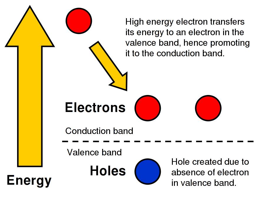
24 Impact ionization
FUNDAMENTALS OF MODERN VLSI DEVICES
 19-13- FUNDAMENTALS OF MODERN VLSI DEVICES YUAN TAUR TAK H. MING CAMBRIDGE UNIVERSITY PRESS Physical Constants and Unit Conversions List of Symbols Preface page xi xiii xxi 1 INTRODUCTION I 1.1 Evolution
Lecture-45. MOS Field-Effect-Transistors Threshold voltage
 Lecture-45 MOS Field-Effect-Transistors 7.4. Threshold voltage In this section we summarize the calculation of the threshold voltage and discuss the dependence of the threshold voltage on the bias applied
NAME: Last First Signature
 UNIVERSITY OF CALIFORNIA, BERKELEY College of Engineering Department of Electrical Engineering and Computer Sciences EE 130: IC Devices Spring 2003 FINAL EXAMINATION NAME: Last First Signature STUDENT
Field-Effect Transistor (FET) is one of the two major transistors; FET derives its name from its working mechanism;
 is one of the two major transistors; FET derives its name from its working mechanism;") Chapter 3 Field-Effect Transistors (FETs) 3.1 Introduction Field-Effect Transistor (FET) is one of the two major transistors; FET derives its name from its working mechanism; The concept has been known
Chapter 3 Field-Effect Transistors (FETs) 3.1 Introduction Field-Effect Transistor (FET) is one of the two major transistors; FET derives its name from its working mechanism; The concept has been known
Lecture 4. MOS transistor theory
 Lecture 4 MOS transistor theory 1.7 Introduction: A MOS transistor is a majority-carrier device, in which the current in a conducting channel between the source and the drain is modulated by a voltage
CHAPTER 3 TWO DIMENSIONAL ANALYTICAL MODELING FOR THRESHOLD VOLTAGE
 49 CHAPTER 3 TWO DIMENSIONAL ANALYTICAL MODELING FOR THRESHOLD VOLTAGE 3.1 INTRODUCTION A qualitative notion of threshold voltage V th is the gate-source voltage at which an inversion channel forms, which
Sub-Threshold Region Behavior of Long Channel MOSFET
 Sub-threshold Region - So far, we have discussed the MOSFET behavior in linear region and saturation region - Sub-threshold region is refer to region where Vt is less than Vt - Sub-threshold region reflects
CONTENTS. 2.2 Schrodinger's Wave Equation 31. PART I Semiconductor Material Properties. 2.3 Applications of Schrodinger's Wave Equation 34
 CONTENTS Preface x Prologue Semiconductors and the Integrated Circuit xvii PART I Semiconductor Material Properties CHAPTER 1 The Crystal Structure of Solids 1 1.0 Preview 1 1.1 Semiconductor Materials
MOSFET Parasitic Elements
 MOSFET Parasitic Elements Three MITs of the ay Components of the source resistance and their influence on g m and R d Gate-induced drain leakage (GIL) and its effect on lowest possible leakage current
6. LDD Design Tradeoffs on Latch-Up and Degradation in SOI MOSFET
 110 6. LDD Design Tradeoffs on Latch-Up and Degradation in SOI MOSFET An experimental study has been conducted on the design of fully depleted accumulation mode SOI (SIMOX) MOSFET with regard to hot carrier
Charge-Based Continuous Equations for the Transconductance and Output Conductance of Graded-Channel SOI MOSFET s
 Charge-Based Continuous Equations for the Transconductance and Output Conductance of Graded-Channel SOI MOSFET s Michelly de Souza 1 and Marcelo Antonio Pavanello 1,2 1 Laboratório de Sistemas Integráveis,
Fundamentals of Power Semiconductor Devices
 В. Jayant Baliga Fundamentals of Power Semiconductor Devices 4y Spri ringer Contents Preface vii Chapter 1 Introduction 1 1.1 Ideal and Typical Power Switching Waveforms 3 1.2 Ideal and Typical Power Device
Session 10: Solid State Physics MOSFET
 Session 10: Solid State Physics MOSFET 1 Outline A B C D E F G H I J 2 MOSCap MOSFET Metal-Oxide-Semiconductor Field-Effect Transistor: Al (metal) SiO2 (oxide) High k ~0.1 ~5 A SiO2 A n+ n+ p-type Si (bulk)
Why Scaling? CPU speed Chip size R, C CPU can increase speed by reducing occupying area.
 Why Scaling? Higher density : Integration of more transistors onto a smaller chip : reducing the occupying area and production cost Higher Performance : Higher current drive : smaller metal to metal capacitance
PHYSICS OF SEMICONDUCTOR DEVICES
 PHYSICS OF SEMICONDUCTOR DEVICES PHYSICS OF SEMICONDUCTOR DEVICES by J. P. Colinge Department of Electrical and Computer Engineering University of California, Davis C. A. Colinge Department of Electrical
International Journal of Scientific & Engineering Research, Volume 6, Issue 2, February-2015 ISSN
 Performance Evaluation and Comparison of Ultra-thin Bulk (UTB), Partially Depleted and Fully Depleted SOI MOSFET using Silvaco TCAD Tool Seema Verma1, Pooja Srivastava2, Juhi Dave3, Mukta Jain4, Priya
Reliability of deep submicron MOSFETs
 Invited paper Reliability of deep submicron MOSFETs Francis Balestra Abstract In this work, a review of the reliability of n- and p-channel Si and SOI MOSFETs as a function of gate length and temperature
value of W max for the device. The at band voltage is -0.9 V. Problem 5: An Al-gate n-channel MOS capacitor has a doping of N a = cm ;3. The oxi
 Prof. Jasprit Singh Fall 2001 EECS 320 Homework 10 This homework is due on December 6 Problem 1: An n-type In 0:53 Ga 0:47 As epitaxial layer doped at 10 16 cm ;3 is to be used as a channel in a FET. A
ECE 340 Lecture 40 : MOSFET I
 ECE 340 Lecture 40 : MOSFET I Class Outline: MOS Capacitance-Voltage Analysis MOSFET - Output Characteristics MOSFET - Transfer Characteristics Things you should know when you leave Key Questions How do
Semiconductor Physics and Devices
 Metal-Semiconductor and Semiconductor Heterojunctions The Metal-Oxide-Semiconductor Field-Effect Transistor (MOSFET) is one of two major types of transistors. The MOSFET is used in digital circuit, because
UNIT-1 Fundamentals of Low Power VLSI Design
 UNIT-1 Fundamentals of Low Power VLSI Design Need for Low Power Circuit Design: The increasing prominence of portable systems and the need to limit power consumption (and hence, heat dissipation) in very-high
97.398*, Physical Electronics, Lecture 21. MOSFET Operation
 97.398*, Physical Electronics, Lecture 21 MOSFET Operation Lecture Outline Last lecture examined the MOSFET structure and required processing steps Now move on to basic MOSFET operation, some of which
EE301 Electronics I , Fall
 EE301 Electronics I 2018-2019, Fall 1. Introduction to Microelectronics (1 Week/3 Hrs.) Introduction, Historical Background, Basic Consepts 2. Rewiev of Semiconductors (1 Week/3 Hrs.) Semiconductor materials
Solid State Devices- Part- II. Module- IV
 Solid State Devices- Part- II Module- IV MOS Capacitor Two terminal MOS device MOS = Metal- Oxide- Semiconductor MOS capacitor - the heart of the MOSFET The MOS capacitor is used to induce charge at the
Two Dimensional Analytical Threshold Voltages Modeling for Short-Channel MOSFET
 Two Dimensional Analytical Threshold Voltages Modeling for Short-Channel MOSFET Sanjeev kumar Singh, Vishal Moyal Electronics & Telecommunication, SSTC-SSGI, Bhilai, Chhatisgarh, India Abstract- The aim
FET(Field Effect Transistor)
") Field Effect Transistor: Construction and Characteristic of JFETs. Transfer Characteristic. CS,CD,CG amplifier and analysis of CS amplifier MOSFET (Depletion and Enhancement) Type, Transfer Characteristic,
Field Effect Transistor: Construction and Characteristic of JFETs. Transfer Characteristic. CS,CD,CG amplifier and analysis of CS amplifier MOSFET (Depletion and Enhancement) Type, Transfer Characteristic,
Channel Engineering for Submicron N-Channel MOSFET Based on TCAD Simulation
 Australian Journal of Basic and Applied Sciences, 2(3): 406-411, 2008 ISSN 1991-8178 Channel Engineering for Submicron N-Channel MOSFET Based on TCAD Simulation 1 2 3 R. Muanghlua, N. Vittayakorn and A.
Power MOSFET Zheng Yang (ERF 3017,
 ECE442 Power Semiconductor Devices and Integrated Circuits Power MOSFET Zheng Yang (ERF 3017, email: yangzhen@uic.edu) Evolution of low-voltage (
Contents. Contents... v. Preface... xiii. Chapter 1 Introduction...1. Chapter 2 Significant Physical Effects In Modern MOSFETs...
 Contents Contents... v Preface... xiii Chapter 1 Introduction...1 1.1 Compact MOSFET Modeling for Circuit Simulation...1 1.2 The Trends of Compact MOSFET Modeling...5 1.2.1 Modeling new physical effects...5
3-D Modelling of the Novel Nanoscale Screen-Grid Field Effect Transistor (SGFET)
") 3-D Modelling of the Novel Nanoscale Screen-Grid Field Effect Transistor (SGFET) Pei W. Ding, Kristel Fobelets Department of Electrical Engineering, Imperial College London, U.K. J. E. Velazquez-Perez
3-D Modelling of the Novel Nanoscale Screen-Grid Field Effect Transistor (SGFET) Pei W. Ding, Kristel Fobelets Department of Electrical Engineering, Imperial College London, U.K. J. E. Velazquez-Perez
Tunneling Field Effect Transistors for Low Power ULSI
 Tunneling Field Effect Transistors for Low Power ULSI Byung-Gook Park Inter-university Semiconductor Research Center and School of Electrical and Computer Engineering Seoul National University Outline
Device design methodology to optimize low-frequency Noise in advanced SOI CMOS technology
 Device design methodology to optimize low-frequency Noise in advanced SOI CMOS technology Prem Prakash Satpathy*, Dr. VijayNath**, Abhinandan Jain*** *Lecturer, Dept. of ECE, Cambridge Institute of Technology,
Semiconductor TCAD Tools
 Device Design Consideration for Nanoscale MOSFET Using Semiconductor TCAD Tools Teoh Chin Hong and Razali Ismail Department of Microelectronics and Computer Engineering, Universiti Teknologi Malaysia,
Semiconductor Devices
 Semiconductor Devices Modelling and Technology Source Electrons Gate Holes Drain Insulator Nandita DasGupta Amitava DasGupta SEMICONDUCTOR DEVICES Modelling and Technology NANDITA DASGUPTA Professor Department
Department of Electrical Engineering IIT Madras
 Department of Electrical Engineering IIT Madras Sample Questions on Semiconductor Devices EE3 applicants who are interested to pursue their research in microelectronics devices area (fabrication and/or
Lecture #29. Moore s Law
 Lecture #29 ANNOUNCEMENTS HW#15 will be for extra credit Quiz #6 (Thursday 5/8) will include MOSFET C-V No late Projects will be accepted after Thursday 5/8 The last Coffee Hour will be held this Thursday
Three Terminal Devices
 Three Terminal Devices - field effect transistor (FET) - bipolar junction transistor (BJT) - foundation on which modern electronics is built - active devices - devices described completely by considering
Digital Electronics. By: FARHAD FARADJI, Ph.D. Assistant Professor, Electrical and Computer Engineering, K. N. Toosi University of Technology
 K. N. Toosi University of Technology Chapter 7. Field-Effect Transistors By: FARHAD FARADJI, Ph.D. Assistant Professor, Electrical and Computer Engineering, K. N. Toosi University of Technology http://wp.kntu.ac.ir/faradji/digitalelectronics.htm
Optical Receivers Theory and Operation
 Optical Receivers Theory and Operation Photo Detectors Optical receivers convert optical signal (light) to electrical signal (current/voltage) Hence referred O/E Converter Photodetector is the fundamental
Prepared by: Dr. Rishi Prakash, Dept of Electronics and Communication Engineering Page 1 of 5
 Microwave tunnel diode Some anomalous phenomena were observed in diode which do not follows the classical diode equation. This anomalous phenomena was explained by quantum tunnelling theory. The tunnelling
Introduction to semiconductor technology
 Introduction to semiconductor technology Outline 7 Field effect transistors MOS transistor current equation" MOS transistor channel mobility Substrate bias effect 7 Bipolar transistors Introduction Minority
4: Transistors Non idealities
 4: Transistors Non idealities Inversion Major cause of non-idealities/complexities: Who controls channel (and how)? Large Body(Substrate) Source Voltage V G V SB - - - - - - - - n+ n+ - - - - - - - - -
MOSFET & IC Basics - GATE Problems (Part - I)
") MOSFET & IC Basics - GATE Problems (Part - I) 1. Channel current is reduced on application of a more positive voltage to the GATE of the depletion mode n channel MOSFET. (True/False) [GATE 1994: 1 Mark]
MOSFET & IC Basics - GATE Problems (Part - I) 1. Channel current is reduced on application of a more positive voltage to the GATE of the depletion mode n channel MOSFET. (True/False) [GATE 1994: 1 Mark]
INTERNATIONAL JOURNAL OF APPLIED ENGINEERING RESEARCH, DINDIGUL Volume 1, No 3, 2010
 Low Power CMOS Inverter design at different Technologies Vijay Kumar Sharma 1, Surender Soni 2 1 Department of Electronics & Communication, College of Engineering, Teerthanker Mahaveer University, Moradabad
3: MOS Transistors. Non idealities
 3: MOS Transistors Non idealities Inversion Major cause of non-idealities/complexities: Who controls channel (and how)? Large Body(Substrate) Source Voltage V G V SB - - - - - - - - n+ n+ - - - - - - -
EE5320: Analog IC Design
 EE5320: Analog IC Design Handout 3: MOSFETs Saurabh Saxena & Qadeer Khan Indian Institute of Technology Madras Copyright 2018 by EE6:Integrated Circuits & Systems roup @ IIT Madras Overview Transistors
Future MOSFET Devices using high-k (TiO 2 ) dielectric
 dielectric") Future MOSFET Devices using high-k (TiO 2 ) dielectric Prerna Guru Jambheshwar University, G.J.U.S. & T., Hisar, Haryana, India, prernaa.29@gmail.com Abstract: In this paper, an 80nm NMOS with high-k (TiO
Future MOSFET Devices using high-k (TiO 2 ) dielectric Prerna Guru Jambheshwar University, G.J.U.S. & T., Hisar, Haryana, India, prernaa.29@gmail.com Abstract: In this paper, an 80nm NMOS with high-k (TiO
Substrate Bias Effects on Drain Induced Barrier Lowering (DIBL) in Short Channel NMOS FETs
 in Short Channel NMOS FETs") Australian Journal of Basic and Applied Sciences, 3(3): 1640-1644, 2009 ISSN 1991-8178 Substrate Bias Effects on Drain Induced Barrier Lowering (DIBL) in Short Channel NMOS FETs 1 1 1 1 2 A. Ruangphanit,
Australian Journal of Basic and Applied Sciences, 3(3): 1640-1644, 2009 ISSN 1991-8178 Substrate Bias Effects on Drain Induced Barrier Lowering (DIBL) in Short Channel NMOS FETs 1 1 1 1 2 A. Ruangphanit,
Analysis and Design of a Low Voltage Si LDMOS Transistor
 International Journal of Latest Research in Engineering and Technology (IJLRET) ISSN: 2454-5031(Online) ǁ Volume 1 Issue 3ǁAugust 2015 ǁ PP 65-69 Analysis and Design of a Low Voltage Si LDMOS Transistor
Design and Analysis of Double Gate MOSFET Devices using High-k Dielectric
 International Journal of Electrical Engineering. ISSN 0974-2158 Volume 7, Number 1 (2014), pp. 53-60 International Research Publication House http://www.irphouse.com Design and Analysis of Double Gate
Depletion-mode operation ( 공핍형 ): Using an input gate voltage to effectively decrease the channel size of an FET
: Using an input gate voltage to effectively decrease the channel size of an FET") Ch. 13 MOSFET Metal-Oxide-Semiconductor Field-Effect Transistor : I D D-mode E-mode V g The gate oxide is made of dielectric SiO 2 with e = 3.9 Depletion-mode operation ( 공핍형 ): Using an input gate voltage
Ch. 13 MOSFET Metal-Oxide-Semiconductor Field-Effect Transistor : I D D-mode E-mode V g The gate oxide is made of dielectric SiO 2 with e = 3.9 Depletion-mode operation ( 공핍형 ): Using an input gate voltage
444 Index. F Fermi potential, 146 FGMOS transistor, 20 23, 57, 83, 84, 98, 205, 208, 213, 215, 216, 241, 242, 251, 280, 311, 318, 332, 354, 407
 Index A Accuracy active resistor structures, 46, 323, 328, 329, 341, 344, 360 computational circuits, 171 differential amplifiers, 30, 31 exponential circuits, 285, 291, 292 multifunctional structures,
Numerical Simulation of a Nanoscale DG N-MOSFET Using SILVACO Software
 Numerical Simulation of a Nanoscale DG N-MOSFET Using SILVACO Software Ahlam Guen Faculty of Technology Tlemcen University Tlemcen,Algeria guenahlam@yahoo.fr Benyounes Bouazza Faculty of Technology. Tlemcen
Design of 45 nm Fully Depleted Double Gate SOI MOSFET
 Design of 45 nm Fully Depleted Double Gate SOI MOSFET 1. Mini Bhartia, 2. Shrutika. Satyanarayana, 3. Arun Kumar Chatterjee 1,2,3. Thapar University, Patiala Abstract Advanced MOSFETS such as Fully Depleted
MOS TRANSISTOR THEORY
 MOS TRANSISTOR THEORY Introduction A MOS transistor is a majority-carrier device, in which the current in a conducting channel between the source and the drain is modulated by a voltage applied to the
Effect of Channel Doping Concentration on the Impact ionization of n- Channel Fully Depleted SOI MOSFET
 International Journal of Engineering Works Kambohwell Publisher Enterprises Vol. 2, Issue 2, PP. 18-22, Feb. 2015 www.kwpublisher.com Effect of Channel Doping Concentration on the Impact ionization of
MASTER OF TECHNOLOGY in VLSI Design & CAD
 ANALYSIS AND DESIGN OF A DRAM CELL FOR LOW LEAKAGE Thesis submitted in partial fulfillment of the requirements for the award of the degree of MASTER OF TECHNOLOGY in VLSI Design & CAD By Rashmi Singh Roll
ECE 440 Lecture 39 : MOSFET-II
 ECE 440 Lecture 39 : MOSFETII Class Outline: MOSFET Qualitative Effective Mobility MOSFET Quantitative Things you should know when you leave Key Questions How does a MOSFET work? Why does the channel mobility
Mechatronics and Measurement. Lecturer:Dung-An Wang Lecture 2
 Mechatronics and Measurement Lecturer:Dung-An Wang Lecture 2 Lecture outline Reading:Ch3 of text Today s lecture Semiconductor 2 Diode 3 4 Zener diode Voltage-regulator diodes. This family of diodes exhibits
EIE209 Basic Electronics. Transistor Devices. Contents BJT and FET Characteristics Operations. Prof. C.K. Tse: T ransistor devices
 EIE209 Basic Electronics Transistor Devices Contents BJT and FET Characteristics Operations 1 What is a transistor? Three-terminal device whose voltage-current relationship is controlled by a third voltage
INTRODUCTION: Basic operating principle of a MOSFET:
 INTRODUCTION: Along with the Junction Field Effect Transistor (JFET), there is another type of Field Effect Transistor available whose Gate input is electrically insulated from the main current carrying
8. Characteristics of Field Effect Transistor (MOSFET)
") 1 8. Characteristics of Field Effect Transistor (MOSFET) 8.1. Objectives The purpose of this experiment is to measure input and output characteristics of n-channel and p- channel field effect transistors
1 8. Characteristics of Field Effect Transistor (MOSFET) 8.1. Objectives The purpose of this experiment is to measure input and output characteristics of n-channel and p- channel field effect transistors
ECE520 VLSI Design. Lecture 2: Basic MOS Physics. Payman Zarkesh-Ha
 ECE520 VLSI Design Lecture 2: Basic MOS Physics Payman Zarkesh-Ha Office: ECE Bldg. 230B Office hours: Wednesday 2:00-3:00PM or by appointment E-mail: pzarkesh@unm.edu Slide: 1 Review of Last Lecture Semiconductor
A perspective on low-power, low-voltage supervisory circuits implemented with SOI technology.
 Silicon-On-Insulator A perspective on low-power, low-voltage supervisory circuits implemented with SOI technology. By Ondrej Subrt The magic term of SOI is attracting a lot of attention in the design of
Photodiode: LECTURE-5
 LECTURE-5 Photodiode: Photodiode consists of an intrinsic semiconductor sandwiched between two heavily doped p-type and n-type semiconductors as shown in Fig. 3.2.2. Sufficient reverse voltage is applied
Performance Evaluation of MISISFET- TCAD Simulation
 Performance Evaluation of MISISFET- TCAD Simulation Tarun Chaudhary Gargi Khanna Rajeevan Chandel ABSTRACT A novel device n-misisfet with a dielectric stack instead of the single insulator of n-mosfet
Lecture 13. Metal Oxide Semiconductor Field Effect Transistor (MOSFET) MOSFET 1-1
 MOSFET 1-1") Lecture 13 Metal Oxide Semiconductor Field Effect Transistor (MOSFET) MOSFET 1-1 Outline Continue MOSFET Qualitative Operation epletion-type MOSFET Characteristics Biasing Circuits and Examples Enhancement-type
Lecture 13 Metal Oxide Semiconductor Field Effect Transistor (MOSFET) MOSFET 1-1 Outline Continue MOSFET Qualitative Operation epletion-type MOSFET Characteristics Biasing Circuits and Examples Enhancement-type
LEAKAGE POWER REDUCTION TECHNIQUES FOR LOW POWER VLSI DESIGN: A REVIEW PAPER
 International Journal Of Advance Research In Science And Engineering http:// LEAKAGE POWER REDUCTION TECHNIQUES FOR LOW POWER VLSI DESIGN: A REVIEW PAPER Raju Hebbale 1, Pallavi Hiremath 2 1,2 Department
Conduction Characteristics of MOS Transistors (for fixed Vds)! Topic 2. Basic MOS theory & SPICE simulation. MOS Transistor
! Topic 2. Basic MOS theory & SPICE simulation. MOS Transistor") Conduction Characteristics of MOS Transistors (for fixed Vds)! Topic 2 Basic MOS theory & SPICE simulation Peter Cheung Department of Electrical & Electronic Engineering Imperial College London (Weste&Harris,
Conduction Characteristics of MOS Transistors (for fixed Vds)! Topic 2 Basic MOS theory & SPICE simulation Peter Cheung Department of Electrical & Electronic Engineering Imperial College London (Weste&Harris,
Topic 2. Basic MOS theory & SPICE simulation
 Topic 2 Basic MOS theory & SPICE simulation Peter Cheung Department of Electrical & Electronic Engineering Imperial College London (Weste&Harris, Ch 2 & 5.1-5.3 Rabaey, Ch 3) URL: www.ee.ic.ac.uk/pcheung/
Conduction Characteristics of MOS Transistors (for fixed Vds) Topic 2. Basic MOS theory & SPICE simulation. MOS Transistor
 Topic 2. Basic MOS theory & SPICE simulation. MOS Transistor") Conduction Characteristics of MOS Transistors (for fixed Vds) Topic 2 Basic MOS theory & SPICE simulation Peter Cheung Department of Electrical & Electronic Engineering Imperial College London (Weste&Harris,
Conduction Characteristics of MOS Transistors (for fixed Vds) Topic 2 Basic MOS theory & SPICE simulation Peter Cheung Department of Electrical & Electronic Engineering Imperial College London (Weste&Harris,
PAPER SOLUTION_DECEMBER_2014_VLSI_DESIGN_ETRX_SEM_VII Prepared by Girish Gidaye
 Q1a) The MOS System under External Bias Depending on the polarity and the magnitude of V G, three different operating regions can be observed for the MOS system: 1) Accumulation 2) Depletion 3) Inversion
Reg. No. : Question Paper Code : B.E./B.Tech. DEGREE EXAMINATION, NOVEMBER/DECEMBER Second Semester
 WK 5 Reg. No. : Question Paper Code : 27184 B.E./B.Tech. DEGREE EXAMINATION, NOVEMBER/DECEMBER 2015. Time : Three hours Second Semester Electronics and Communication Engineering EC 6201 ELECTRONIC DEVICES
SRM INSTITUTE OF SCIENCE AND TECHNOLOGY (DEEMED UNIVERSITY)
") SRM INSTITUTE OF SCIENCE AND TECHNOLOGY (DEEMED UNIVERSITY) QUESTION BANK I YEAR B.Tech (II Semester) ELECTRONIC DEVICES (COMMON FOR EC102, EE104, IC108, BM106) UNIT-I PART-A 1. What are intrinsic and
SRM INSTITUTE OF SCIENCE AND TECHNOLOGY (DEEMED UNIVERSITY) QUESTION BANK I YEAR B.Tech (II Semester) ELECTRONIC DEVICES (COMMON FOR EC102, EE104, IC108, BM106) UNIT-I PART-A 1. What are intrinsic and
cost and reliability; power considerations were of secondary importance. In recent years. however, this has begun to change and increasingly power is
 CHAPTER-1 INTRODUCTION AND SCOPE OF WORK 1.0 MOTIVATION In the past, the major concern of the VLSI designer was area, performance, cost and reliability; power considerations were of secondary importance.
Performance investigations of novel dual-material gate (DMG) MOSFET with dielectric pockets (DP)
 MOSFET with dielectric pockets (DP)") Science in China Series E: Technological Sciences 2009 SCIENCE IN CHINA PRESS www.scichina.com tech.scichina.com Performance investigations of novel dual-material gate (DMG) MOSFET with dielectric pockets
Science in China Series E: Technological Sciences 2009 SCIENCE IN CHINA PRESS www.scichina.com tech.scichina.com Performance investigations of novel dual-material gate (DMG) MOSFET with dielectric pockets
Influence of Fin Shape and Temperature on Conventional and Strained MuGFETs Analog Parameters
 02 (49)-AF:Modelo-AF 8/20/11 6:25 AM Page 94 Influence of Fin Shape and Temperature on Conventional and Strained MuGFETs Analog Parameters Rudolf Theoderich Bühler 1, Renato Giacomini 1,2 and João Antonio
4 principal of JNTU college of Eng., JNTUH, Kukatpally, Hyderabad, A.P, INDIA
 Efficient Power Management Technique for Deep-Submicron Circuits P.Sreenivasulu 1, Ch.Aruna 2 Dr. K.Srinivasa Rao 3, Dr. A.Vinaya babu 4 1 Research Scholar, ECE Department, JNTU Kakinada, A.P, INDIA. 2
Review Energy Bands Carrier Density & Mobility Carrier Transport Generation and Recombination
 Review Energy Bands Carrier Density & Mobility Carrier Transport Generation and Recombination Current Transport: Diffusion, Thermionic Emission & Tunneling For Diffusion current, the depletion layer is
Session 3: Solid State Devices. Silicon on Insulator
 Session 3: Solid State Devices Silicon on Insulator 1 Outline A B C D E F G H I J 2 Outline Ref: Taurand Ning 3 SOI Technology SOl materials: SIMOX, BESOl, and Smart Cut SIMOX : Synthesis by IMplanted
FET. Field Effect Transistors ELEKTRONIKA KONTROL. Eka Maulana, ST, MT, M.Eng. Universitas Brawijaya. p + S n n-channel. Gate. Basic structure.
 FET Field Effect Transistors ELEKTRONIKA KONTROL Basic structure Gate G Source S n n-channel Cross section p + p + p + G Depletion region Drain D Eka Maulana, ST, MT, M.Eng. Universitas Brawijaya S Channel
2014, IJARCSSE All Rights Reserved Page 1352
 Volume 4, Issue 3, March 2014 ISSN: 2277 128X International Journal of Advanced Research in Computer Science and Software Engineering Research Paper Available online at: www.ijarcsse.com Double Gate N-MOSFET
Lecture 15. Field Effect Transistor (FET) Wednesday 29/11/2017 MOSFET 1-1
 Wednesday 29/11/2017 MOSFET 1-1") Lecture 15 Field Effect Transistor (FET) Wednesday 29/11/2017 MOSFET 1-1 Outline MOSFET transistors Introduction to MOSFET MOSFET Types epletion-type MOSFET Characteristics Comparison between JFET and
Lecture 15 Field Effect Transistor (FET) Wednesday 29/11/2017 MOSFET 1-1 Outline MOSFET transistors Introduction to MOSFET MOSFET Types epletion-type MOSFET Characteristics Comparison between JFET and
EE 5611 Introduction to Microelectronic Technologies Fall Thursday, September 04, 2014 Lecture 02
 EE 5611 Introduction to Microelectronic Technologies Fall 2014 Thursday, September 04, 2014 Lecture 02 1 Lecture Outline Review on semiconductor materials Review on microelectronic devices Example of microelectronic
THE primary motivation for scaling complementary metal
 IEEE TRANSACTIONS ON DEVICE AND MATERIALS RELIABILITY, VOL. 5, NO. 3, SEPTEMBER 2005 509 Shielded Channel Double-Gate MOSFET: A Novel Device for Reliable Nanoscale CMOS Applications AliA.Orouji,Member,
Solid State Device Fundamentals
 Solid State Device Fundamentals 4.4. Field Effect Transistor (MOSFET) ENS 463 Lecture Course by Alexander M. Zaitsev alexander.zaitsev@csi.cuny.edu Tel: 718 982 2812 4N101b 1 Field-effect transistor (FET)
Field-Effect Transistors
 R L 2 Field-Effect Transistors 2.1 BAIC PRINCIPLE OF JFET The eld-effect transistor (FET) is an electric- eld (voltage) operated transistor, developed as a semiconductor equivalent of the vacuum-tube device,
EE70 - Intro. Electronics
 EE70 - Intro. Electronics Course website: ~/classes/ee70/fall05 Today s class agenda (November 28, 2005) review Serial/parallel resonant circuits Diode Field Effect Transistor (FET) f 0 = Qs = Qs = 1 2π
EJERCICIOS DE COMPONENTES ELECTRÓNICOS. 1 er cuatrimestre
 EJECICIOS DE COMPONENTES ELECTÓNICOS. 1 er cuatrimestre 2 o Ingeniería Electrónica Industrial Juan Antonio Jiménez Tejada Índice 1. Basic concepts of Electronics 1 2. Passive components 1 3. Semiconductors.
Lecture 18: Photodetectors
 Lecture 18: Photodetectors Contents 1 Introduction 1 2 Photodetector principle 2 3 Photoconductor 4 4 Photodiodes 6 4.1 Heterojunction photodiode.................... 8 4.2 Metal-semiconductor photodiode................
IMPROVED CURRENT MIRROR OUTPUT PERFORMANCE BY USING GRADED-CHANNEL SOI NMOSFETS
 IMPROVED CURRENT MIRROR OUTPUT PERFORMANCE BY USING GRADED-CHANNEL SOI NMOSFETS Marcelo Antonio Pavanello *, João Antonio Martino and Denis Flandre 1 Laboratório de Sistemas Integráveis Escola Politécnica
COLLECTOR DRAIN BASE GATE EMITTER. Applying a voltage to the Gate connection allows current to flow between the Drain and Source connections.
 MOSFETS Although the base current in a transistor is usually small (< 0.1 ma), some input devices (e.g. a crystal microphone) may be limited in their output. In order to overcome this, a Field Effect Transistor
EECE 481. MOS Basics Lecture 2
 EECE 481 MOS Basics Lecture 2 Reza Molavi Dept. of ECE University of British Columbia reza@ece.ubc.ca Slides Courtesy : Dr. Res Saleh (UBC), Dr. D. Sengupta (AMD), Dr. B. Razavi (UCLA) 1 PN Junction and
Chapter 6: Field-Effect Transistors
 Chapter 6: Field-Effect Transistors Islamic University of Gaza Dr. Talal Skaik MOSFETs MOSFETs have characteristics similar to JFETs and additional characteristics that make then very useful. There are
FIELD EFFECT TRANSISTOR (FET) 1. JUNCTION FIELD EFFECT TRANSISTOR (JFET)
 1. JUNCTION FIELD EFFECT TRANSISTOR (JFET)") FIELD EFFECT TRANSISTOR (FET) The field-effect transistor (FET) is a three-terminal device used for a variety of applications that match, to a large extent, those of the BJT transistor. Although there
FIELD EFFECT TRANSISTOR (FET) The field-effect transistor (FET) is a three-terminal device used for a variety of applications that match, to a large extent, those of the BJT transistor. Although there
Investigation and Modelling of the Floating Body Effects and Surface Recombination on SOS MOSFETs
 Investigation and Modelling of the Floating Body Effects and Surface Recombination on SOS MOSFETs Student: Tom (Chien-Ju) Chu Department of Electrical and Computer Engineering, University of Queensland.
Fin-Shaped Field Effect Transistor (FinFET) Min Ku Kim 03/07/2018
 Min Ku Kim 03/07/2018") Fin-Shaped Field Effect Transistor (FinFET) Min Ku Kim 03/07/2018 ECE 658 Sp 2018 Semiconductor Materials and Device Characterizations OUTLINE Background FinFET Future Roadmap Keeping up w/ Moore s Law
Fin-Shaped Field Effect Transistor (FinFET) Min Ku Kim 03/07/2018 ECE 658 Sp 2018 Semiconductor Materials and Device Characterizations OUTLINE Background FinFET Future Roadmap Keeping up w/ Moore s Law
SYED AMMAL ENGINEERING COLLEGE
 SYED AMMAL ENGINEERING COLLEGE (Approved by the AICTE, New Delhi, Govt. of Tamilnadu and Affiliated to Anna University, Chennai) Established in 1998 - An ISO 9001:2008 Certified Institution Dr. E.M.Abdullah
UNIT 3: FIELD EFFECT TRANSISTORS
 FIELD EFFECT TRANSISTOR: UNIT 3: FIELD EFFECT TRANSISTORS The field effect transistor is a semiconductor device, which depends for its operation on the control of current by an electric field. There are
ECE 340 Lecture 37 : Metal- Insulator-Semiconductor FET Class Outline:
 ECE 340 Lecture 37 : Metal- Insulator-Semiconductor FET Class Outline: Metal-Semiconductor Junctions MOSFET Basic Operation MOS Capacitor Things you should know when you leave Key Questions What is the