EUVL Development in JAPAN
|
|
|
- Francis Higgins
- 5 years ago
- Views:
Transcription

1 EUVL Workshop 2010, June24, Maui EUVL Development in JAPAN ~ Challenge, Idea, and Latest Achievement ~ Iwao Nishiyama 1
2 EUVL Development in Japan Light Source Exposure Tool Metrology Mask & Resist Integration ASET EUV Basic Technologies Supported by NEDO ASET Wavefront measurement Mask blank inspection Supported by NEDO Leading Project (LPP source) Supported by MEXT EUVA Source Pj Supported by NED EUVA Tool Pj Supported by NEDO Mask/Resist Process (R&D by companies) Resist Supported by NEDO SFET Tool Development(R&D by company) EUV1 Wavefront measurement Wavefront measurement Supported by NEDO R&D by company High Reliability Source Supported by NEDO High Power Source R & D by company Mask Supported by NEDO Lithography/Mask R&D by company National Foundation Company Pj 2
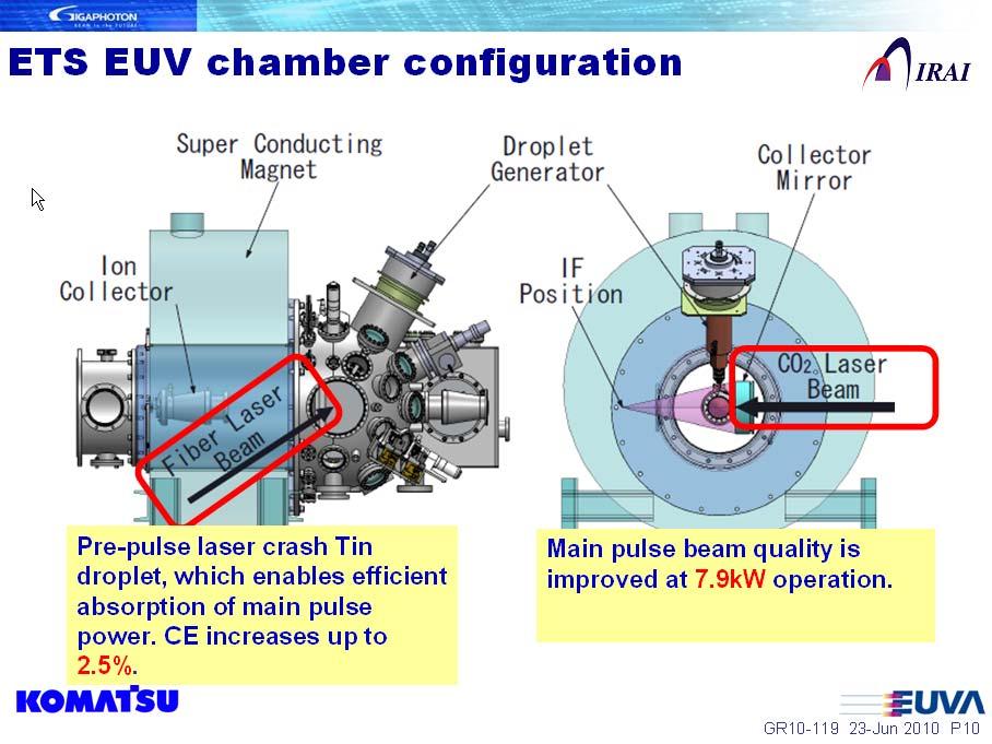
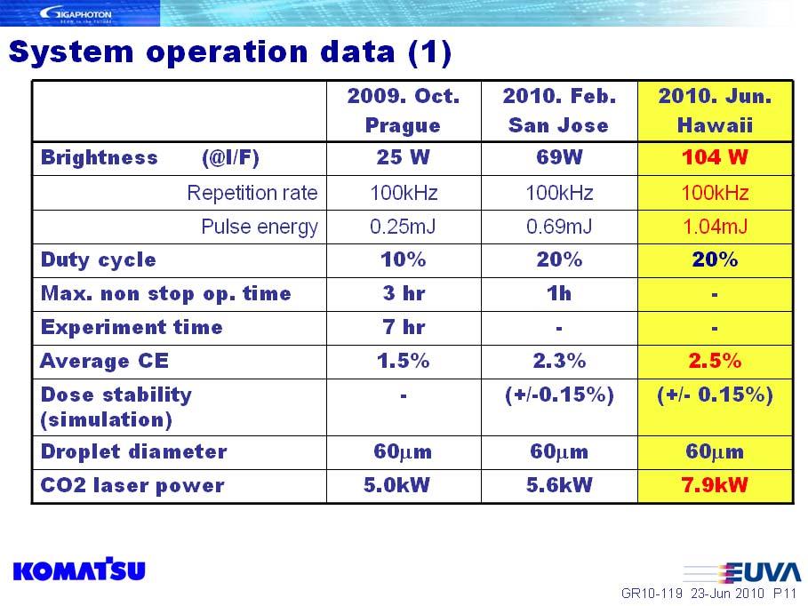
3 Source 3


 High CE of Tin target was")
")
4 First proposal of Tin Target G.O Sullivan and P.K.Carroll J. Opt. Soc. Am. 71 (1981) 227 4d-4f narrow band emission 50 Sn neutral absorption 13.5 nm 54 Xe Tomie, EUVL Workshop 2000 (San Francisco) High CE of Tin target was firstly proposed. Tanuma, EUVL Symposium 2006 (Barcelona) Charge selective spectra were directly measured. Tokyo metropolitan University 4
![Conversion efficiency of CO2 LPP vs YAG LPP Conversion Efficiency [arb. Units] 1.0 0.5 CO 2 LPP vs YAG LPP 0 10 9 10 10 10 11 10 12 10 13 Laser Intensity [W/cm 2 ] Okada, Jpn. J. Appl. Phys.](/docs-images/82/86815557/images/5-0.jpg "(2004) L585 Tanaka, Appl. Phys. Lett. 87 (2005) 041503. Electron Temperature [ev] Density-temperature map of 13.")
5 Conversion efficiency of CO2 LPP vs YAG LPP Conversion Efficiency [arb. Units] CO 2 LPP vs YAG LPP Laser Intensity [W/cm 2 ] Okada, Jpn. J. Appl. Phys. (2004) L585 Tanaka, Appl. Phys. Lett. 87 (2005) Electron Temperature [ev] Density-temperature map of 13.5-nm EUV conversion efficiency 4% 3% 2% 1% Ion density [/cm 3 ] Laser Intensity [W/cm 2 ] W/cm 2 1μm CE=1.43% W/cm μm CE=2.22% K. Nishihara, EUVL Symposium 2004 (Miyazaki) Feasibility of CO2 laser driven LPP was firstly demonstrated. 5
6 6
7 7
8 Optics 8
 543 (nm rms) 0.10 0.")
 measured (05/05/25) 0 200 400 600 800 1000 Accumulation number Target: 0.")
9 Metrology for aspherical mirror Visible PDI for High Accuracy High precision interferometer for production PDI: Point diffraction interferometer K. Ota, Proc. SPIE 4343 (2001) 543 (nm rms) Reproducibilit y measured (05/03/23) measured (05/05/25) Accumulation number Target: 0.05nm rms New-concept interferometers were developed for λ/30 projection optics 9


10 At-wavelength wave-front metrology of optics Purpose:Development of standard for WFE metrology 3 m in Diameter, 20 ton in Weight EUV Illumination PDI LSI Gratings Test Optics Projection 1000mm 30mm First Pin-hole 650nm PDI 干渉像 Vacuum Pump Camera Schematic View of 6 Mirror System The System was installed at Hyogo Pref. Univ. Accuracy of 0.1nm rms was achieved Large Window and 2nd Pinhole of 50-80nm Interference fringes obtained by PDI 10
11 Tool 11


 5914 H. Nagata, Jpn. J. Appl. Phys.")
 In-line 5X NA0.")
 102 5X NA0.")
12 1986 NTT EUVL Tool development in Japan - Small Field Tool SORTEC 50 nm hp 5X, 8X Schwartz Child, 11nm/12.4 nm H. Kinoshita, Proc. Fall Mtg. Jpn Soc. Appl. Phys. (1986) H. Kinoshita, J. Vac. Sci. Technol. B7(1989) ASET(HiNA) Nikon 32X Schwartz Child, 13 nm / 4.5 nm H. Oizumi, 1993 Jpn J Appl. Phys. 32 (1993) 5914 H. Nagata, Jpn. J. Appl. Phys. 33 (1994) L Selete(SFET) Exposure chamber Canon Source (Xe DPP) In-line 5X NA0.32 T. Oshino, Proc. SPIE 5037 (2003) 75 H. Oizumi, Proc. SPIE 5751 (2005) 102 5X NA0.32 H. Tanaka, EUVL Symposium 2007 (Sapporo) K. Tawarayama, Jap. J. Appl. Phys. 47 (2008)
 2008 Nikon-Selete(EUV1) Vacuum")


 7597 I.")
13 EUVL Tool development in Japan -Full Field Tool HIT(ETS) 2008 Nikon-Selete(EUV1) Vacuum chamber Optics housing W & M alignment system Mask M1 M3 M2 Optical Bbase a P laplate Wafer Vibration Isolation Bench 5X, NA 0.1, SR Source 3 aspheric mirror system 4X, NA 0.25, Xe-DPP 6 aspheric mirror system T. Watanabe, Jpn. J. Appl. Phys. 36 (1997) 7597 I. Mori, Proc. SPIE 6921 (2008)
14 Mask 14


15 EUV Mask Development in Selete Mask Infrastructure Particle free mask handling Actinic Blank Inspection EUV 13.5 nm Pattern Inspection DUV 199 nm Pattern Repair FIB Double pod MPE-tool Blank Inspection M defects/transfer 0.002particlse/transfer Mask pattern Printed Image Mask defect printability Phase defect Pattern Defect Defect repair Semi standardization of double pod Contamination control シリカ系 H C H O H CH O H O Si H CH Si O C C CH 2 水素率高 C CH C H C C CH CH H C C CH CH CH CH C C C C CH H 重量密度低 CH O C CH O CH C H Si H CH O H 2 C 不飽和芳香族鎖状コンタミネーション膜 C O OH C SiH C C CH CH CH C C C 炭素率高 H C CH C C CH C C C CH 黒鉛化率低 O C CH C O CC CH CH CH C C CH C C H 重量密度高 O C C C Si O Si H Si O O O Si C Si O Si キャップ層 Si Si Si O Si Si O Si O O O OSi 自然酸化膜 Model コンタミ薄膜のモデル例 of carbon contamination Carbon analysis Printability Cleaning Resist outgas 15

16 Sensitivity of Pattern defect inspection Low reflectivity absorber(r4%) Allowable defect size(10 % CD change) Base pattern hp32nm hp128nm (hp128nm) hp27nm hp108nm (hp108nm) hp22nm hp88nm (hp88nm) Defect type Edge extrusion extension Edge intrusion intrusion Edge extrusion extension Edge intrusion Edge extrusion extension Edge intrusion Illumination C-pol. P-pol. C-pol. P-pol. C-pol. P-pol. C-pol. P-pol. C-pol. P-pol. C-pol. P-pol. Defect size [nm] (Square root of area) Defect size:35nm LR absorber (R4% R4%) ML (Mo/Si 40pairs) Substrate *LR= Low Reflectivity LR*- TaSi (51nm) CrN buffer (10 nm) Si cap hp32nm hp32nm (128nm@mask) (128nm@mask) Both Both of of c- c- and and P- P- polarizations polarizations have have enough enough sensitivity sensitivity hp27nm hp27nm (108nm@mask) (108nm@mask) p-polarization p-polarization has has enough enough sensitivity sensitivity hp22nm hp22nm (( 88nm@mask) 88nm@mask) p-polarization p-polarization has has potential potential for for hp22nm hp22nm application, application, but but further further improvement improvement is is needed needed Defect size:41nm 16


 [nm] Line Width [nm] 36 34 32 30 28 26 24 22 20 18 16 14 12")
![Edge Clear Defect Simulation Measured 0 4 8 12 16 20 24 Defect Size (1x) [nm]](/docs-images/82/86815557/images/17-3.jpg "Using the CD Averaging Method, simulated results were verified by actual PD")
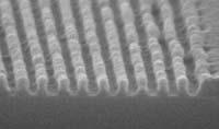
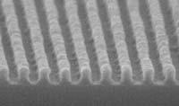
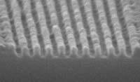
17 Defect printability test by programmed Defect Multi-shot images ware averaged to reduce resist LER Mask Defect Exposure Shot1 Shot2 Printed images Shot7 Hp32 Hp32 nm(7 nm(7 shots shots averaging) averaging) average (Edge intrusion) Comparison between Simulation and Printed CD change Space Width [nm] Edge Opaque Defect Simulation Measured Defect Size (1x) [nm] Line Width [nm] Edge Clear Defect Simulation Measured Defect Size (1x) [nm] Using the CD Averaging Method, simulated results were verified by actual PD printing test. 17
 PC Ellipsoidal Mirror Incident EUV light Scattered EUV light CCD camera Zr Filter EUV light source (DPP, 1.")
18 Actinic Blank Inspection POC tool (MIRAI I and II) (Top view) Full-field Inspection tool (Front view) YAG Laser 532nm, 10Hz Collector Mirror 6025 Mask Blank Zr Filter EUV LD Tape target Schwarzschild Optics (20x or 26x, NA=0.2) PC Ellipsoidal Mirror Incident EUV light Scattered EUV light CCD camera Zr Filter EUV light source (DPP, 1.9 khz) Illumination optics Vibration isolator CCD camera Schwarzschild optics (26X) 6025 Mask blank Mask stage In house LPP EUV light source (10 Hz) Mask stage stroke: X,Y: 10 mm,2 mm (Manual operation) Static imaging mode Commercial available EUV source (1.9 khz) Mask stage stroke: X,Y: 169 mm,169 mm (Automatic controlled) TDI mode & Static imaging mode 18
19 Detection probability improvement 1Q Q Q 2010 One FOV (0.5mm sq.) Full-field of mask blank Threshold Noise Filter Defect capture rate (%) false defect Defect volume (nm 3 ) 80,000 false defects 0 1 false defect 1 false defect Defect volume (nm 3 ) Defect volume (nm 3 ) 19


20 Multilayer phase defect Height 2.5 nm Defect Map of Multilayered Blank Substrate width Multilayer A Wx:108nm, Wy:102nm, H:1.9nm D Wx:40nm, Wy:43nm, H: 1.8nm E nmh, 60 nmw 20 Wx:19nm, Wy:20nm, H: 1.1nm Detection of Programmed defects 0 22nm 32nm C Rank 12 Defect signal intensity Rank 11 Rank 10 Rank 9 Rank 8 Rank 7 Rank 6 Rank 5 Rank 4 Rank 3 Rank 2 Rank Frequency Critical for hp 32 nm Critical for hp 22 nm Defects critical for hp 32 nm Defects critical for hp 22 nm Wx:28nm, Wy:16nm, H: 2.8nm 20
21 Resist 21
22 Change of resist chemistry by excitation energy Absorption cross section(10-18 cm 2 ) Absorption spectra of simple organic molecule DUV METHANE 2ETHANE 3 PROPANE 4BUTANE PHOTON ENERGY(eV) DUV resist EUV resist Transmittance is a key factor for DUV lithography. ( nm) Reaction occurs by electronic excitation ( Photochemistry) EUV All DUV and EB resists technologies can be used for EUV lithography Reaction occurs by ionization of molecules (radiation chemistry) 22
 204")
23 S. Tagawa et. al. SPIE 3999 (2000)


 35")


 N")


24 Pattern Collapse Improvement by New Developer Short-range LWR: 3σ(nm) at hp32nm HO SSR3 SSR4+Process 5.0 SSR4 N SSR E size of hp32nm (mj/cm 2 ) Sensitivity - LWR TMAH 0.26N (Tetramethyl Ammonium Hydrooxide) - hp 26 nm hp 25 nm hp 24 nm Swelling Resolution limit (nm) Pattern collapse SSR4 SSR3 SSR4+Process SSR2 New Developer TBAH 0.26N (Tetrabutyl Ammonium Hydrooxide) N + HO E size of hp32nm (mj/cm 2 ) Sensitivity - Resolution 24


25 Latest performance of EUV resist hp 28 nm hp 26 nm hp 24 nm hp 22 nm hp 21 nm hp 20 nm SSR4 Dose: 11.9mJ/cm 2 LWR: 7.2nm hp 19 nm SMR569 Dose: 16.0mJ/cm 2 LWR: 5.4nm SFET NA0.3 Illumination: X-slit 50nm Thick. Developer: TBAH 25
 M100 Protecting group:")

")
:")
: LWR(nm): hp")

 After Etching")
 /SiO 2 (4nm t )/Si")
 hp 32 nm hp 28 nm")

26 Molecular Resist(Fullaren derivatives) M100 Protecting group: bulky ester SMR567 based on M100 M100 bulky E/BBI nf 30wt%/TOA 3wt% Substrate: under layer F (UL F) 20nm Film thickness: 50nm SFET (x slit) PAB 110 /PEB 110 Dev.: TMAH 0.26N 30 sec SMR567 Dose(mJ/cm 2 ): LWR(nm): hp 26 nm SMR601 Dose(mJ/cm 2 ): LWR(nm): hp 25 nm SMR567: 保護基の最適化 SMR601: 保護比率の増加 Litho-pattern Resist(60nm t ) /UL(20nm t ) After Etching Resist(60nm t ) /UL(20nm t ) /Poly-Si(50nm t ) /SiO 2 (4nm t )/Si Cross sectiona view befere/after etching(smr ) hp 32 nm hp 28 nm hp 26 nm Normarized Etch-rate Etcher: U 8150 (Hitachi) Condition :Cl 2, 0.4Pa, 500W 1.00 ArF resist (dry) 0.81 SMR377 (PHS-tBOC) 0.53 MET-2D 0.37 SMR567 (Fullerene) 26
27 Full Field Exposure 27


 X Y x y Mean 1.")
28 hp 28 nm 35 nm ホール Performance of EUV1 (1) CD accuracy In-field homogenuity Mean = 29.5 nm 3σ = 3.7 nm 16.7 mm 22.1 mm Mean = 37.0 nm 3σ = 3.3 nm Frequency Frequency Overlay accuracy Via 1 to Metal 1 Overlay accuracy from V1 to M1 (nm) Metal 2 to Via Overlay accuracy from M2 to V1 (nm) X Y x y Mean σ (nm) X Y x y Mean σ (nm) 28

29 Performance of EUV1 (2) Resolution performance by dipole illumination 26mm σ=0.8 σ=0.4 SSR4: 45 nm thick Dose: 11 mj/cm 2 29
![Yield improvement of hp 3X nm PL-TEG 100% 80% 43 nm hp 38 nm hp 35 nm hp 1 st RUN ( 09/1) tiny bridge SSR3 Yield Yield was was improved improved by by resist resist performance performance Yield [%]](/docs-images/82/86815557/images/30-0.jpg "60% 40% collapse 20% SMR73 0% 0.1 1 10 100 1000 10000 length [mm] 100% 2 nd RUN ( 09/6) SSR4 80% Yield [%] 60% 40% 43 nm hp 38 nm hp 35 nm hp 3 rd RUN ( 09/10) HP vs. Yield (V line 0.")
30 Yield improvement of hp 3X nm PL-TEG 100% 80% 43 nm hp 38 nm hp 35 nm hp 1 st RUN ( 09/1) tiny bridge SSR3 Yield Yield was was improved improved by by resist resist performance performance Yield [%] 60% 40% collapse 20% SMR73 0% length [mm] 100% 2 nd RUN ( 09/6) SSR4 80% Yield [%] 60% 40% 43 nm hp 38 nm hp 35 nm hp 3 rd RUN ( 09/10) HP vs. Yield (V line 0.7 mm) 20% 100% 100% Yield [%] 90% 80% 70% 60% 50% 40% 30% 20% 10% 0% 55 1st Run 2nd Run 3rd Run HP [nm] % 80% length [mm] 60% Yield [%] 40% 43 nm hp 20% 38 nm hp 35 nm hp 0% 32 nm hp length [mm] 30
31 Summary History of Japan EUVL development was reviewed. Source power is approaching 100 W level based on understanding of plasma physics under the collaboration with university and national laboratories. Wavefront error of optics is drastically improved by introduction of new metrology techniques in this decade, and become to satisfy the requirement to pre-production exposure tool. EUV1 shows resolution of 22 nm hp with dipole illumination. Mask infrastructure is now developing at Selete. Signal to noise ratio of actinic blank inspection tool (ABI) is improved. We applied ABI tool to whole-area bank inspection, and successfully demonstrated the sensitivity as small to 1.1nmH and 20nmW defect. DUV (199 nm)-based pattern inspection technique is applicable to hp 2X by using polarized illumination and low reflectance absorber material. Defect printability are studied using above infrastructures and calculation. Resist performance has improved steady based on the improvement of materials and processing technologies. We are now developing the α-stage EUVL processing, and will be transferred to β-stage processing in next phase and also manufacturing in company. We are now developing BEOL-TEG(hp35nm) process, and PL-TEG(hp3Xnm and hp2xnm) process. We learn the issues for high volume production. 31
32 Acknowledgement A part of technologies shown in this presentation are developed by the support of NEDO (New Energy and Industrial Technology Development Organization) under the management of METI (Ministry of Economy, Trade and Industry). The author thanks to all co-workers for assistance of presentation. 32
Recent Activities of the Actinic Mask Inspection using the EUV microscope at Center for EUVL
 Recent Activities of the Actinic Mask Inspection using the EUV microscope at Center for EUVL Takeo Watanabe, Tetsuo Harada, and Hiroo Kinoshita Center for EUVL, University of Hyogo Outline 1) EUV actinic
Recent Development Activities on EUVL at ASET
 Title Recent Development Activities on at ASET Shinji Okazaki ASET Laboratory 2 nd International Workshop on 1 Overall Development Plan 98 99 00 01 02 03 04 05 06 07 08 ASET Basic Technologies 100% Government
Akira Miyake, Chidane Ouchi, International EUVL Symposium, October , Kobe Slide 1
 Development Status of Canon s EUVL Exposure Tool Akira Miyake, Chidane Ouchi, Hideki Morishima, and Hiroyoshi Kubo Canon Inc. International EUVL Symposium, October 18 2010, Kobe Slide 1 Outline EUVL Exposure
Nikon EUVL Development Progress Update
 Nikon EUVL Development Progress Update Takaharu Miura EUVL Symposium September 29, 2008 EUVL Symposium 2008 @Lake Tahoe T. Miura September 29, 2008 Slide 1 Presentation Outline 1. Nikon EUV roadmap 2.
2009 International Workshop on EUV Lithography
 Contents Introduction Absorber Stack Optimization Non-flatness Correction Blank Defect and Its Mitigation Wafer Printing Inspection Actinic Metrology Cleaning and Repair Status Remaining Issues in EUV
Characterization of Actinic Mask Blank Inspection for Improving Sensitivity
 Characterization of Actinic Mask Blank Inspection for Improving Sensitivity Yoshihiro Tezuka, Toshihiko Tanaka, Tsuneo Terasawa, Toshihisa Tomie * M-ASET, Tsukuba, Japan * M-ASRC, AIST, Tsukuba, Japan
TSMC Property. EUV Lithography. The March toward HVM. Anthony Yen. 9 September TSMC, Ltd
 EUV Lithography The March toward HVM Anthony Yen 9 September 2016 1 1 st EUV lithography setup and results, 1986 Si Stencil Mask SR W/C Multilayer Coating Optics λ=11 nm, provided by synchrotron radiation
National Projects on Semiconductor in NEDO
 National Projects on Semiconductor in NEDO June 17, 2011 Toru Nakayama New Energy and Industrial Technology Development Organization (NEDO), Japan Contents About NEDO NEDO s projects for semiconductor
Defect printability of thin absorber mask in EUV lithography with refined LER resist
 [#5, MA] Defect printability of thin absorber mask in EUV lithography with refined LER resist Takashi Kamo, Hajime Aoyama, Yukiyasu Arisawa, Mihoko Kijima, Toshihiko Tanaka and Osamu Suga e-mail: kamo.takashi@selete.co.jp
EUV Interference Lithography in NewSUBARU
 EUV Interference Lithography in NewSUBARU Takeo Watanabe 1, Tae Geun Kim 2, Yasuyuki Fukushima 1, Noki Sakagami 1, Teruhiko Kimura 1, Yoshito Kamaji 1, Takafumi Iguchi 1, Yuuya Yamaguchi 1, Masaki Tada
R&D Status and Key Technical and Implementation Challenges for EUV HVM
 R&D Status and Key Technical and Implementation Challenges for EUV HVM Sam Intel Corporation Agenda Requirements by Process Node EUV Technology Status and Gaps Photoresists Tools Reticles Summary 2 Moore
Development of ultra-fine structure t metrology system using coherent EUV source
 2009 International Workshop On EUV Lithography, July 13-17,2009 Development of ultra-fine structure t metrology system using coherent EUV source University of Hyogo 1, Hiroo Kinoshita 1,3, Tetuo Harada
EUV Lithography Transition from Research to Commercialization
 EUV Lithography Transition from Research to Commercialization Charles W. Gwyn and Peter J. Silverman and Intel Corporation Photomask Japan 2003 Pacifico Yokohama, Kanagawa, Japan Gwyn:PMJ:4/17/03:1 EUV
EUV Actinic Blank Inspection Tool Development
 EUV Actinic Blank Inspection Tool Development EUVL Symposium 2011 Hiroki Miyai 1, Tomohiro Suzuki 1, Kiwamu Takehisa 1, Haruhiko Kusunose 1, Takeshi Yamane 2, Tsuneo Terasawa 2, Hidehiro Watanabe 2, Soichi
Update on 193nm immersion exposure tool
 Update on 193nm immersion exposure tool S. Owa, H. Nagasaka, Y. Ishii Nikon Corporation O. Hirakawa and T. Yamamoto Tokyo Electron Kyushu Ltd. January 28, 2004 Litho Forum 1 What is immersion lithography?
EUVL Activities in China. Xiangzhao Wang Shanghai Inst. Of Opt. and Fine Mech. Of CAS. (SIOM) Shanghai, China.
 Shanghai, China.") EUVL Activities in China Xiangzhao Wang Shanghai Inst. Of Opt. and Fine Mech. Of CAS. (SIOM) Shanghai, China. wxz26267@siom.ac.cn Projection Optics Imaging System Surface Testing Optical Machining ML Coating
EUVL Activities in China Xiangzhao Wang Shanghai Inst. Of Opt. and Fine Mech. Of CAS. (SIOM) Shanghai, China. wxz26267@siom.ac.cn Projection Optics Imaging System Surface Testing Optical Machining ML Coating
The Coherent EUV Scatterometry Microscope for Actinic Mask Inspection and Metrology
 The Coherent EUV Scatterometry Microscope for Actinic Mask Inspection and Metrology Tetsuo Harada* 1,3, Masato Nakasuji 1,3, Teruhiko Kimura 1,3, Yutaka Nagata 2,3, Takeo Watanabe 1,3, Hiroo Kinoshita
EUVL Activities in China
 2014 EUVL Workshop EUVL Activities in China Yanqiu Li, Zhen Cao Beijing Institute of Technology (BIT) Email: liyanqiu@bit.edu.cn Activities only refer to published papers June 25, 2014 OUTLINE Overview
Laser-Produced Sn-plasma for Highvolume Manufacturing EUV Lithography
 Panel discussion Laser-Produced Sn-plasma for Highvolume Manufacturing EUV Lithography Akira Endo * Extreme Ultraviolet Lithography System Development Association Gigaphoton Inc * 2008 EUVL Workshop 11
Shooting for the 22nm Lithography Goal with the. Coat/Develop Track. SOKUDO Lithography Breakfast Forum 2010 July 14 (L1)
") Shooting for the 22nm Lithography Goal with the Coat/Develop Track SOKUDO Lithography Breakfast Forum 2010 July 14 (L1) Three (3) different exposure options for 22nm: Public External (L1) MAPPER Lithography
Shooting for the 22nm Lithography Goal with the Coat/Develop Track SOKUDO Lithography Breakfast Forum 2010 July 14 (L1) Three (3) different exposure options for 22nm: Public External (L1) MAPPER Lithography
Light Sources for High Volume Metrology and Inspection Applications
 Light Sources for High Volume Metrology and Inspection Applications Reza Abhari International Workshop on EUV and Soft X- Ray Sources November 9-11, 2015, Dublin, Ireland Reza S. Abhari 11/10/15 1 Inspection
Challenges of EUV masks and preliminary evaluation
 Challenges of EUV masks and preliminary evaluation Naoya Hayashi Electronic Device Laboratory Dai Nippon Printing Co.,Ltd. EUV Mask Workshop 2004 1 Contents Recent Lithography Options on Roadmap Challenges
Discovering Electrical & Computer Engineering. Carmen S. Menoni Professor Week 3 armain.
 Discovering Electrical & Computer Engineering Carmen S. Menoni Professor Week 3 http://www.engr.colostate.edu/ece103/semin armain.html TOP TECH 2012 SPECIAL REPORT IEEE SPECTRUM PAGE 28, JANUARY 2012 P.E.
2008 European EUVL. EUV activities the EUVL shop future plans. Rob Hartman
 2008 European EUVL EUV activities the EUVL shop future plans Rob Hartman 2007 international EUVL Symposium 28-31 October 2007 2008 international EUVL Symposium 28 Sapporo, September Japan 1 October 2008
Lithography Roadmap. without immersion lithography. Node Half pitch. 248nm. 193nm. 157nm EUVL. 3-year cycle: 2-year cycle: imec 2005
 Lithography Roadmap without immersion lithography Node Half pitch 180 nm 130 nm 90 nm 65 nm 45 nm 32 nm 22 nm 250 nm 180 nm 130 nm 90 nm 65 nm 45 nm 32 nm 248nm 193nm 157nm EUVL 3-year cycle: 2-year cycle:
Shot noise and process window study for printing small contacts using EUVL. Sang Hun Lee John Bjorkohlm Robert Bristol
 Shot noise and process window study for printing small contacts using EUVL Sang Hun Lee John Bjorkohlm Robert Bristol Abstract There are two issues in printing small contacts with EUV lithography (EUVL).
EUVL getting ready for volume introduction
 EUVL getting ready for volume introduction SEMICON West 2010 Hans Meiling, July 14, 2010 Slide 1 public Outline ASML s Lithography roadmap to support Moore s Law Progress on 0.25NA EUV systems Progress
Light Sources for EUV Mask Metrology. Heiko Feldmann, Ulrich Müller
 Light Sources for EUV Mask Metrology Heiko Feldmann, Ulrich Müller Dublin, October 9, 2012 Agenda 1 2 3 4 Actinic Metrology in Mask Making The AIMS EUV Concept Metrology Performance Drivers and their Relation
S26 Basic research on 6.x nm EUV generation by laser produced plasma
 S26 Basic research on 6.x nm EUV generation by laser produced plasma Tsukasa Hori, Tatsuya Yanagida, Hitoshi Nagano, Yasunori Wada, Soumagne Georg, Junichi Fujimoto*, Hakaru Mizoguchi* e-mail : tsukasa_hori@komatsu.co.jp
Laser Produced Plasma Light Source for HVM-EUVL
 Laser Produced Plasma Light Source for HVM-EUVL Akira Endo, Hideo Hoshino, Takashi Suganuma, Krzysztof Nowak, Tatsuya Yanagida, Takayuki Yabu, Takeshi Asayama, Yoshifumi Ueno, Masato Moriya, Masaki Nakano,
NIST EUVL Metrology Programs
 NIST EUVL Metrology Programs S.Grantham, C. Tarrio, R.E. Vest, Y. Barad, S. Kulin, K. Liu and T.B. Lucatorto National Institute of Standards and Technology (NIST) Gaithersburg, MD USA L. Klebanoff and
EUVL Challenges for Next Generation Devices
 EUVL Challenges for Next Generation Devices Center for Semiconductor Research & Development Advanced Lithography Process Technology Dept. Tatsuhiko Higashiki Contents Device Roadmap and Lithography Extendibility
Reliable High Power EUV Source Technology for HVM: LPP or DPP? Vivek Bakshi, Ph.D. EUV Litho, Inc.
 Reliable High Power EUV Source Technology for HVM: LPP or DPP? Vivek Bakshi, Ph.D. EUV Litho, Inc. Presentation Outline Source Technology Requirements Source Technology Performance DPP LPP Technology Trend
Progress in full field EUV lithography program at IMEC
 Progress in full field EUV lithography program at IMEC A.M. Goethals*, G.F. Lorusso*, R. Jonckheere*, B. Baudemprez*, J. Hermans*, F. Iwamoto 1, B.S. Kim 2, I.S. Kim 2, A. Myers 3, A. Niroomand 4, N. Stepanenko
Present Status of the ASET At-Wavelength Phase-Shifting Point Diffraction Interferometer
 Present Status of the ASET At-Wavelength Phase-Shifting Point Diffraction Interferometer Katsumi Sugisaki Yucong Zhu a Yoshio Gomei amasahito Niibe b Takeo Watanabe b Hiroo Kinoshita b a Association of
Lithography. 3 rd. lecture: introduction. Prof. Yosi Shacham-Diamand. Fall 2004
 Lithography 3 rd lecture: introduction Prof. Yosi Shacham-Diamand Fall 2004 1 List of content Fundamental principles Characteristics parameters Exposure systems 2 Fundamental principles Aerial Image Exposure
EUV Resist Materials and Process for 16 nm Half Pitch and Beyond
 EUV Workshop 2013 June 13, 2013 EUV Resist Materials and Process for 16 nm Half Pitch and Beyond Yoshi Hishiro JSR Micro Inc. No13-2400-056 Challenge for EUV Resist & JSR approaches EUV Resist Resolution,
Progress towards Actinic Patterned Mask Inspection. Oleg Khodykin
 Progress towards Actinic Patterned Mask Inspection Oleg Khodykin Outline Status (technical) of EUV Actinic Reticle Inspection program Xe based LPP source as bright and reliable solution Requirements Choice
EUV: Status and Challenges Ahead International Workshop on EUVL, Maui 2010
 EUV: Status and Challenges Ahead International Workshop on EUVL, Maui 2010 Jos Benschop Public Agenda Roadmap Status Challenges Summary & conclusion Slide 2 Public Resolution (half pitch) "Shrink" [nm]
EUVL Activities in China
 EUVL Activities in China Yanqiu Li Beijing Institute of Technology (BIT) Phone/Fax: 010-68918443 Email: liyanqiu@bit.edu.cn June 13, 2013 HI Contents Overview of EUVL in China System EUVL Optics EUV Metrology
Mask Technology Development in Extreme-Ultraviolet Lithography
 Mask Technology Development in Extreme-Ultraviolet Lithography Anthony Yen September 6, 2013 Projected End of Optical Lithography 2013 TSMC, Ltd 1976 1979 1982 1985 1988 1991 1994 1997 2000 2003 2007 2012
Section 2: Lithography. Jaeger Chapter 2 Litho Reader. The lithographic process
 Section 2: Lithography Jaeger Chapter 2 Litho Reader The lithographic process Photolithographic Process (a) (b) (c) (d) (e) (f) (g) Substrate covered with silicon dioxide barrier layer Positive photoresist
 http://goldberg.lbl.gov 1 To EUV or not to EUV? That is the question. Do we need EUV interferometry and EUV optical testing? 17 Things you need to know about perfecting EUV optics. 2 The main things you
Progresses in NIL Template Fabrication Naoya Hayashi
 Progresses in NIL Template Fabrication Naoya Hayashi Electronic Device Operations Dai Nippon Printing Co., Ltd. Contents 1. Introduction Motivation NIL mask fabrication process 2. NIL mask resolution improvement
Collector development with IR suppression and EUVL optics refurbishment at RIT
 Collector development with IR suppression and EUVL optics refurbishment at RIT Yuriy Platonov, Michael Kriese, Raymond Crucet, Yang Li, Vladimir Martynov, Licai Jiang, Jim Rodriguez Rigaku Innovative Technologies
Section 2: Lithography. Jaeger Chapter 2 Litho Reader. EE143 Ali Javey Slide 5-1
 Section 2: Lithography Jaeger Chapter 2 Litho Reader EE143 Ali Javey Slide 5-1 The lithographic process EE143 Ali Javey Slide 5-2 Photolithographic Process (a) (b) (c) (d) (e) (f) (g) Substrate covered
Optical Lithography. Keeho Kim Nano Team / R&D DongbuAnam Semi
 Optical Lithography Keeho Kim Nano Team / R&D DongbuAnam Semi Contents Lithography = Photolithography = Optical Lithography CD : Critical Dimension Resist Pattern after Development Exposure Contents Optical
Japan Update. EUVA (Extreme Ultraviolet Lithography System Development Association) Koichi Toyoda. SOURCE TWG 2 March, 2005 San Jose
 Koichi Toyoda. SOURCE TWG 2 March, 2005 San Jose") 1 Japan Update EUVA (Extreme Ultraviolet Lithography System Development Association) Koichi Toyoda SOURCE TWG 2 March, 2005 San Jose Outline 2 EUVA LPP at Hiratsuka R&D Center GDPP at Gotenba Branch Lab.
1 Japan Update EUVA (Extreme Ultraviolet Lithography System Development Association) Koichi Toyoda SOURCE TWG 2 March, 2005 San Jose Outline 2 EUVA LPP at Hiratsuka R&D Center GDPP at Gotenba Branch Lab.
Section 2: Lithography. Jaeger Chapter 2. EE143 Ali Javey Slide 5-1
 Section 2: Lithography Jaeger Chapter 2 EE143 Ali Javey Slide 5-1 The lithographic process EE143 Ali Javey Slide 5-2 Photolithographic Process (a) (b) (c) (d) (e) (f) (g) Substrate covered with silicon
UV Nanoimprint Stepper Technology: Status and Roadmap. S.V. Sreenivasan Sematech Litho Forum May 14 th, 2008
 UV Nanoimprint Stepper Technology: Status and Roadmap S.V. Sreenivasan Sematech Litho Forum May 14 th, 2008 Overview Introduction Stepper technology status: Patterning and CD Control Through Etch Alignment
EUV Light Source The Path to HVM Scalability in Practice
 EUV Light Source The Path to HVM Scalability in Practice Harald Verbraak et al. (all people at XTREME) 2011 International Workshop on EUV and Soft X-ray Sources Nov. 2011 Today s Talk o LDP Technology
Comparison of actinic and non-actinic inspection of programmed defect masks
 Comparison of actinic and non-actinic inspection of programmed defect masks Funded by Kenneth Goldberg, Anton Barty Hakseung Han*, Stefan Wurm*, Patrick Kearney, Phil Seidel Obert Wood*, Bruno LaFontaine
5. Lithography. 1. photolithography intro: overall, clean room 2. principle 3. tools 4. pattern transfer 5. resolution 6. next-gen
 5. Lithography 1. photolithography intro: overall, clean room 2. principle 3. tools 4. pattern transfer 5. resolution 6. next-gen References: Semiconductor Devices: Physics and Technology. 2 nd Ed. SM
EUVL Scanners Operational at Chipmakers. Skip Miller Semicon West 2011
 EUVL Scanners Operational at Chipmakers Skip Miller Semicon West 2011 Outline ASML s Lithography roadmap to support Moore s Law Progress on NXE:3100 (0.25NA) EUV systems Progress on NXE:3300 (0.33NA) EUV
Progress & actual performance of the Selete EUV1
 Progress & actual performance of the Selete EUV1 Kazuo Tawarayama*, Hajime Aoyama, Kentaro Matsunaga, Shunko Magoshi Selete Suigen Kyoh, Yumi Nakajima, Satoshi Tanaka, TOSHIBA 1 Outline Introduction Tool
Sub-50 nm period patterns with EUV interference lithography
 Microelectronic Engineering 67 68 (2003) 56 62 www.elsevier.com/ locate/ mee Sub-50 nm period patterns with EUV interference lithography * a, a a b b b H.H. Solak, C. David, J. Gobrecht, V. Golovkina,
Fundamental Aspect of Photosensitized Chemically Amplified Resist How to overcome RLS trade-off
 Fundamental Aspect of Photosensitized Chemically Amplified Resist How to overcome RLS trade-off Seiichi Tagawa, Akihiro Oshima (Osaka University), Seiji Nagahara (Tokyo Electron Ltd.), Hisashi Nakagawa
SEMATECH Defect Printability Studies
 Accelerating the next technology revolution SEMATECH Defect Printability Studies Il Yong Jang 1, Jenah Harris-Jones 1, Ranganath Teki 1, Vibhu Jindal 1, Frank Goodwin 1 Masaki Satake 2, Ying Li 2, Danping
Optics for EUV Lithography
 Optics for EUV Lithography Dr. Sascha Migura, Carl Zeiss SMT GmbH, Oberkochen, Germany 2018 EUVL Workshop June 13 th, 2018 Berkeley, CA, USA The resolution of the optical system determines the minimum
A novel High Average Power High Brightness Soft X-ray Source using a Thin Disk Laser System for optimized Laser Produced Plasma Generation
 A novel High Average Power High Brightness Soft X-ray Source using a Thin Disk Laser System for optimized Laser Produced Plasma Generation I. Mantouvalou, K. Witte, R. Jung, J. Tümmler, G. Blobel, H. Legall,
Photolithography II ( Part 2 )
") 1 Photolithography II ( Part 2 ) Chapter 14 : Semiconductor Manufacturing Technology by M. Quirk & J. Serda Saroj Kumar Patra, Department of Electronics and Telecommunication, Norwegian University of Science
1 Photolithography II ( Part 2 ) Chapter 14 : Semiconductor Manufacturing Technology by M. Quirk & J. Serda Saroj Kumar Patra, Department of Electronics and Telecommunication, Norwegian University of Science
EUV lithography: today and tomorrow
 EUV lithography: today and tomorrow Vadim Banine, Stuart Young, Roel Moors Dublin, October 2012 Resolution/half pitch, "Shrink" [nm] EUV DPT ArFi ArF KrF Industry roadmap towards < 10 nm resolution Lithography
Fabrication and alignment of 10X-Schwarzschild optics for F2X experiments
 Fabrication and alignment of 10X-Schwarzschild optics for F2X experiments a, Michael Shumway b,e, Lou Marchetti d, Donald Phillion c, Regina Soufli c, Manish Chandhok a, Michael Goldstein a, and Jeff Bokor
Process Optimization
 Process Optimization Process Flow for non-critical layer optimization START Find the swing curve for the desired resist thickness. Determine the resist thickness (spin speed) from the swing curve and find
1 st /2nd generation Laser-Produced Plasma source system for HVM EUV lithography
 1 st /2nd generation Laser-Produced Plasma source system for HVM EUV lithography Hakaru Mizoguchi*1, Tamotsu Abe, Yukio Watanabe, Takanobu Ishihara, Takeshi Ohta,Tsukasa Hori, Tatsuya Yanagida, Hitoshi
TECHNOLOGY ROADMAP 2006 UPDATE LITHOGRAPHY FOR
 INTERNATIONAL TECHNOLOGY ROADMAP FOR SEMICONDUCTORS 2006 UPDATE LITHOGRAPHY THE ITRS IS DEVISED AND INTENDED FOR TECHNOLOGY ASSESSMENT ONLY AND IS WITHOUT REGARD TO ANY COMMERCIAL CONSIDERATIONS PERTAINING
Computational Lithography Requirements & Challenges for Mask Making. Naoya Hayashi, Dai Nippon Printing Co., Ltd
 Computational Lithography Requirements & Challenges for Mask Making Naoya Hayashi, Dai Nippon Printing Co., Ltd Contents Introduction Lithography Trends Computational lithography options More Complex OPC
k λ NA Resolution of optical systems depends on the wavelength visible light λ = 500 nm Extreme ultra-violet and soft x-ray light λ = 1-50 nm
 Resolution of optical systems depends on the wavelength visible light λ = 500 nm Spatial Resolution = k λ NA EUV and SXR microscopy can potentially resolve full-field images with 10-100x smaller features
Lecture 7. Lithography and Pattern Transfer. Reading: Chapter 7
 Lecture 7 Lithography and Pattern Transfer Reading: Chapter 7 Used for Pattern transfer into oxides, metals, semiconductors. 3 types of Photoresists (PR): Lithography and Photoresists 1.) Positive: PR
Eun-Jin Kim, GukJin Kim, Seong-Sue Kim*, Han-Ku Cho*, Jinho Ahn**, Ilsin An, and Hye-Keun Oh
 Eun-Jin Kim, GukJin Kim, Seong-Sue Kim*, Han-Ku Cho*, Jinho Ahn**, Ilsin An, and Hye-Keun Oh Lithography Lab. Department of Applied Physics, Hanyang University, Korea *Samsung Electronics Co., LTD. Korea
MICROCHIP MANUFACTURING by S. Wolf
 MICROCHIP MANUFACTURING by S. Wolf Chapter 19 LITHOGRAPHY II: IMAGE-FORMATION and OPTICAL HARDWARE 2004 by LATTICE PRESS CHAPTER 19 - CONTENTS Preliminaries: Wave- Motion & The Behavior of Light Resolution
Scope and Limit of Lithography to the End of Moore s Law
 Scope and Limit of Lithography to the End of Moore s Law Burn J. Lin tsmc, Inc. 1 What dictate the end of Moore s Law Economy Device limits Lithography limits 2 Litho Requirement of Critical Layers Logic
EUVL: Challenges to Manufacturing Insertion
 EUVL: Challenges to Manufacturing Insertion Obert R Wood II International Workshop on EUV Lithography CXRO, LBNL, Berkeley, California 14 June 2017 EUV Critical Issues List EUV Critical Issues, as identified
Registration performance on EUV masks using high-resolution registration metrology
 Registration performance on EUV masks using high-resolution registration metrology Steffen Steinert a, Hans-Michael Solowan a, Jinback Park b, Hakseung Han b, Dirk Beyer a, Thomas Scherübl a a Carl Zeiss
KrF EXCIMER LASER LITHOGRAPHY TECHNOLOGY FOR 64MDRAM
 Journa' of Photopolymer Science and Technology Volume 4, Number 3 (1991) 361-369 KrF EXCIMER LASER LITHOGRAPHY TECHNOLOGY FOR 64MDRAM MASAYUKI ENDO, YOSHIYUKI TAM, TOSHIKI YABU, SHOZO OKADA MASARU SASAGO
EUV lithography: status, future requirements and challenges
 EUV lithography: status, future requirements and challenges EUVL Dublin Vadim Banine with the help of Rudy Peters, David Brandt, Igor Fomenkov, Maarten van Kampen, Andrei Yakunin, Vladimir Ivanov and many
Zoneplate lenses for EUV microscopy. EUVL workshop 2009 Iacopo Mochi, Kenneth A. Goldberg, Erik H. Anderson, Sungmin Huh
 Zoneplate lenses for EUV microscopy EUVL workshop 2009 Iacopo Mochi, Kenneth A. Goldberg, Erik H. Anderson, Sungmin Huh Iacopo Mochi, Kenneth A. Goldberg, Erik H. Anderson Lawrence Berkeley National Laboratory
CD-SEM for 65-nm Process Node
 CD-SEM for 65-nm Process Node 140 CD-SEM for 65-nm Process Node Hiroki Kawada Hidetoshi Morokuma Sho Takami Mari Nozoe OVERVIEW: Inspection equipment for 90-nm and subsequent process nodes is required
Micro- and Nano-Technology... for Optics
 Micro- and Nano-Technology...... for Optics 3.2 Lithography U.D. Zeitner Fraunhofer Institut für Angewandte Optik und Feinmechanik Jena Printing on Stones Map of Munich Stone Print Contact Printing light
Photon Diagnostics. FLASH User Workshop 08.
 Photon Diagnostics FLASH User Workshop 08 Kai.Tiedtke@desy.de Outline What kind of diagnostic tools do user need to make efficient use of FLASH? intensity (New GMD) beam position intensity profile on the
Acceleration of EUV Resist Development with EB Tool
 C/N:1220710068 Acceleration of Resist Development with Tool Takeyoshi Mimura, Takako Suzuki, Makiko Irie, Takeshi Iwai TOKYO OHKA KOGYO CO., LTD. Advanced Material Development Division 1 2007 L Symposium
Lecture 5. Optical Lithography
 Lecture 5 Optical Lithography Intro For most of microfabrication purposes the process (e.g. additive, subtractive or implantation) has to be applied selectively to particular areas of the wafer: patterning
EE143 Fall 2016 Microfabrication Technologies. Lecture 3: Lithography Reading: Jaeger, Chap. 2
 EE143 Fall 2016 Microfabrication Technologies Lecture 3: Lithography Reading: Jaeger, Chap. 2 Prof. Ming C. Wu wu@eecs.berkeley.edu 511 Sutardja Dai Hall (SDH) 1-1 The lithographic process 1-2 1 Photolithographic
Diffractive optical elements and their potential role in high efficiency illuminators
 Diffractive optical elements and their potential role in high efficiency illuminators Patrick Naulleau Farhad Salmassi, Eric Gullikson, Erik Anderson Lawrence Berkeley National Laboratory Patrick Naulleau
Copyright 2000, Society of Photo-Optical Instrumentation Engineers This paper was published in Optical Microlithography XIII, Volume 4000 and is made
 Copyright 00, Society of Photo-Optical Instrumentation Engineers This paper was published in Optical Microlithography XIII, Volume 4000 and is made available as an electronic reprint with permission of
The End of Thresholds: Subwavelength Optical Linewidth Measurement Using the Flux-Area Technique
 The End of Thresholds: Subwavelength Optical Linewidth Measurement Using the Flux-Area Technique Peter Fiekowsky Automated Visual Inspection, Los Altos, California ABSTRACT The patented Flux-Area technique
AOARD REPORT The Photomask Japan '94 Held 22 April 94 at Kawasaki Science Park, Kanagawa, Japan
 > AOARD-TR-94-22 AOARD REPORT The Photomask Japan '94 Held 22 April 94 at Kawasaki Science Park, Kanagawa, Japan 22 April 1994 S. J. Yakura AOARD The Photomask Japan '94 symposium, the first photomask
Semiconductor Manufacturing Technology. Semiconductor Manufacturing Technology. Photolithography: Resist Development and Advanced Lithography
 Semiconductor Manufacturing Technology Michael Quirk & Julian Serda October 2001 by Prentice Hall Chapter 15 Photolithography: Resist Development and Advanced Lithography Eight Basic Steps of Photolithography
Actinic Review of EUV Masks: Status and Recent Results of the AIMS TM EUV System
 Actinic Review of EUV Masks: Status and Recent Results of the AIMS TM EUV System Sascha Perlitz a, Jan Hendrik Peters a, Markus Weiss b, Dirk Hellweg b, Renzo Capelli b, Krister Magnusson b, Matt Malloy
Lithography. Development of High-Quality Attenuated Phase-Shift Masks
 Lithography S P E C I A L Development of High-Quality Attenuated Phase-Shift Masks by Toshihiro Ii and Masao Otaki, Toppan Printing Co., Ltd. Along with the year-by-year acceleration of semiconductor device
Towards an affordable Cost of Ownership for EUVL. Melissa Shell Principal Engineer & Program Manager, EUVL Research Components Research October 2006
 Towards an affordable Cost of Ownership for EUVL Melissa Shell Principal Engineer & Program Manager, EUVL Research Components Research October 2006 1 Robert Bristol Heidi Cao Manish Chandhok Michael Leeson
X-ray generation by femtosecond laser pulses and its application to soft X-ray imaging microscope
 X-ray generation by femtosecond laser pulses and its application to soft X-ray imaging microscope Kenichi Ikeda 1, Hideyuki Kotaki 1 ' 2 and Kazuhisa Nakajima 1 ' 2 ' 3 1 Graduate University for Advanced
Novel EUV Resist Development for Sub-14nm Half Pitch
 EUV Workshop 2015 Maui, HI P64 Novel EUV Resist Development for Sub-14nm Half Pitch Yoshi Hishiro JSR Micro Inc. EUV Workshop, June 17, 2015 1 Contents Requirement for sub-14nm HP EUV resist JSR strategy
Device Fabrication: Photolithography
 Device Fabrication: Photolithography 1 Objectives List the four components of the photoresist Describe the difference between +PR and PR Describe a photolithography process sequence List four alignment
High Power CO 2 Laser, EUVA
 High Power CO 2 Laser, EUVA Akira Endo Extreme Ultraviolet Lithography System Development Association EUVA, Japan EUV Source Workshop 6 May, 2007 Baltimore, MD, USA Ver. 1.0 Acknowledgments This work was
Bridging the Gap Between Tools & Applications
 EUV Workshop, Dublin 7-9 November 2011 The EUV Laser Program at the University of Bern Bridging the Gap Between Tools & Applications D. Bleiner, J.E. Balmer, F. Staub, J. Fei, L. Masoudnia, M. Ruiz Universität
Water-Window Microscope Based on Nitrogen Plasma Capillary Discharge Source
 2015 International Workshop on EUV and Soft X-Ray Sources Water-Window Microscope Based on Nitrogen Plasma Capillary Discharge Source T. Parkman 1, M. F. Nawaz 2, M. Nevrkla 2, M. Vrbova 1, A. Jancarek
450mm patterning out of darkness Backend Process Exposure Tool SOKUDO Lithography Breakfast Forum July 10, 2013 Doug Shelton Canon USA Inc.
 450mm patterning out of darkness Backend Process Exposure Tool SOKUDO Lithography Breakfast Forum 2013 July 10, 2013 Doug Shelton Canon USA Inc. Introduction Half Pitch [nm] 2013 2014 2015 2016 2017 2018
* AIT-5: Maskless, High-NA, Immersion, EUV, Imprint
 Advanced Issues and Technology (AIT) Modules Purpose: Explain the top advanced issues and concepts in optical projection printing and electron-beam lithography. AIT-1: LER and CAR AIT-2: Resolution Enhancement
EUV Multilayer Fabrication
 EUV Multilayer Fabrication Rigaku Innovative Technologies Inc. Yuriy Platonov, Michael Kriese, Jim Rodriguez ABSTRACT: In this poster, we review our use of tools & methods such as deposition flux simulation