UV Nanoimprint Stepper Technology: Status and Roadmap. S.V. Sreenivasan Sematech Litho Forum May 14 th, 2008
|
|
|
- Joan Sims
- 5 years ago
- Views:
Transcription

1 UV Nanoimprint Stepper Technology: Status and Roadmap S.V. Sreenivasan Sematech Litho Forum May 14 th, 2008
2 Overview Introduction Stepper technology status: Patterning and CD Control Through Etch Alignment and Overlay Defect Control Throughput Stepper roadmap Summary
3 Step & Flash Imprint Lithography (S-FIL) High resolution fused silica template, coated with release layer Template Step 1: Dispense drops Planarization layer Substrate Imprint fluid dispenser Low viscosity fluid (Si-containing for S-FIL, Organic for S-FIL/R) Step 2: Lower template and fill pattern Step 3: Polymerize imprint fluid with UV exposure Template very low imprint pressure < 1/20 atmosphere at room temp Planarization layer Substrate Same Process Used for Step & Repeat and Whole Substrate Patterning Planarization layer Substrate Step 4: Separate template from substrate Template Planarization layer Substrate Step & Repeat
4 Applications Summary S-FIL is an enabling technology for manufacture of nano-scale features below 50nm Low cost Technology extendable to less than 10nm Opportunity from multiple and diverse markets High brightness LED s, hard disk drives; relaxed overlay requirements; whole substrate patterning Semiconductors; tight overlay requirement; stepper
5 Overview Introduction Stepper technology status: Patterning and CD Control Through Etch Alignment and Overlay Defect Control Throughput Stepper roadmap Summary
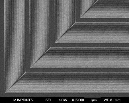
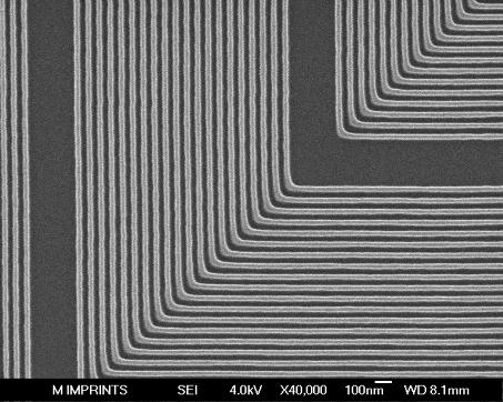
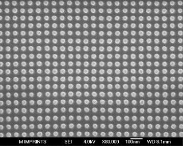
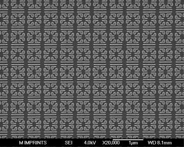
6 Imprint Resolution: 32nm Half Pitch VSB PG
7 CD Budget for Imprint Lithography (Proposed) CDU T = {(CDU M ) 2 + (CDU I ) 2 + (CDU E ) 2 } ½ Table: CDU Budget Elements (in nm 3σ) HP CDU T CDU M CDU E CDU I 32nm 3.2nm 2.5nm 1.75nm 1nm 22nm 2.2nm 1.75nm 1nm 0.9nm To achieve the CDU E of < 1nm, 3σ (for 22nm half-pitch, see Table 1), the total residual layer variation should be <5nm, 3σ

8 Drop Dispense Approach Can handle pattern density variations Compensate for systematic process variations Can achieve tight control over residual layer variation More drops for denser pattern areas Feature Height of 75nm for 30nm features RLT = 10nm mean


9 Transfer and Residual Layer Thickness Measurements 1 nm adhesion layer thickness measurement Ultra-thin adhesion layer Residual layer mean <20nm and thickness variation to < 6 nm TIR MII Metrosol Mean: 1.09nm Sigma: 0.05nm Max: 1.22nm Min: 0.94nm x, y (mm) Residual Layer Thickness (nm) Average Std Dev Min Max Range Residual layer thickness fully populated wafer Position # nm HP


10 Etch: Critical Dimension and Line Edge Roughness At imprint CD = 36.2 ± 1.1 nm LER = 2.9 nm Descum CD = 34.6 ± 1.4 nm LER = 2.5 nm Hardmask etch CD = 34.7 ± 1.0 nm LER = 2.8 nm O2 strip CD = 36.7 ± 1.4 nm LER = 2.9 nm Critical dimension is maintained at ~36 nm at the end of the process. Line edge roughness (LER) is maintained at ~2.9 nm.
11 Overview Introduction Stepper technology status: Patterning and CD Control Through Etch Alignment and Overlay Defect Control Throughput Stepper roadmap Summary
 Target Acquisition Resolution Test 0.2 0.15 0.1 0.")
12 Alignment and Overlay Alignment is achieved using matched Moiré fringe patterns on both template and substrate based on a technique originally developed for X-ray proximity printing at MIT Imprint fluid lubricates movement and dampens vibration Align mechanics Template Substrate <100nm Magnification mechanics Substrate Template d(phase) Target Acquisition Resolution Test dx(nm)-template
13 Field-To-Field Alignment System One of Eight Interferometric Moiré Alignment Technique (i-mat) Cameras Imprint Mask Alignment Marks Imprint area Wafer Technology originally developed for proximity x-ray (Moon, Smith et al., JVST, 1998)
14 Representative Alignment Data (From Four Corners) Four corner alignment data over the wafer represents basic machine precision in X, Y, Theta, MagX, MagY and Ortho directions: 5nm 3sigma in X 6nm 3sigma in Y

15 Multi-Machine Mix-and-Match Overlay Results Mix and match overlay performance with two different 193nm scanners has been demonstrated Overlay metrology performed using an industry standard KT overlay tool. 32 fields per wafer, 81 positions per field Achieved sub 20nm, 3σ results Challenges to move to sub- 10nm overlay appear to be engineering related.
 (μ+3σ) of 11nm in X and 15nm in Y ~100 overlay metrology marks per")
16 Matched Machine Overlay Results ~15nm (μ+3σ) Matched machine overlay (MMO) (μ+3σ) of 11nm in X and 15nm in Y ~100 overlay metrology marks per field
17 Imprint to Photo Overlay Budget Components J Other Process Distortions (CMP, Film Depositions, Etc.) G Template/Mask Pattern Generation Distortion E Thermal In-Plane Template Distortions A X- Y- Alignment Noise (Machine Noise) D B Full Mix-and-Match Process Overlay (FM&MPO) Mix-and-Match, Multi- Template/Mask Overlay (M&MMTO) Single Machine Overlay (SMO) Field Alignment Accuracy MagX, MagY, Ortho Noise (Mag Actuator Noise) H Distortion Due to Tool to Tool Template/Mask Chuck Shape Difference F Thermal In-Plane Wafer Distortions C i-mat Moiré Alignment Metrology Noise I Distortion Due to Imprio to Photo Tool Wafer Chuck Shape Difference Temperature Control Machine Precision K Photo Tool Lens & Scan Speed Matching Distortion
18 Overview Introduction Stepper technology status: Patterning and CD Control Alignment and Overlay Defect Control Throughput Stepper roadmap Summary
19 S-FIL Defectivity 1. Template Fab Defects Template 4. Bubbles 2. Material Contaminants 3. Front Side Particles Planarization layer Substrate 5. Back Side Particles Template Planarization layer Substrate Planarization layer Substrate 6. Improper Release Template Planarization layer Substrate 7. Post-Imprint Fall-On Particles
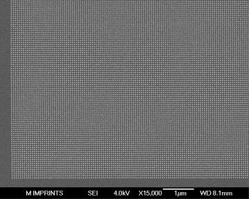
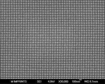
20 Defect Inspection of nm HP Patterns Imprint mask processes, inspection technology, and imprint technology are all at the leading edge at 32nm HP Very challenging to quantify imprint-specific defectivity at 32nm HP Early results are very promising 300 mm wafers imprinted with an imprint mask containing nm halfpitch features and 26 x 32 mm field Field: 16 X 13 cell array Cell: containing inspected Line Blocks

21 KT-eS32 Inspection Results Total Defects Captured by KT - es32 False counts removed Imprinted 300 mm wafer 5 fields were inspected with a KT-eS32 35 nm pixel 416,000 Line-Block features were inspected < 0.1% of the Line Blocks were found to have defects Feature Area Open Area Missing Lines Line Break Write Error Line Shift Line Collapse


22 Random Defects Defects captured only once in the five inspected fields < 0.002% Line Blocks had random defects The Feature Area defects are not truly random, these were only captured once The line collapse defect is probably due to post-imprint contamination by fluid. The source of the Line Shift defect is unknown. Line Shift Feature Area Random Defects Captured by KT- es32 Line Collapse Line Shift Defect Missing Lines


23 E-beam Die-to-Database Inspection NanoGeometry Research Inc. Acc. Voltage: V Probe current: 500pA to 10nA Resolution: 3 nm to 20 nm Sampling rate: 200 M pixel/sec Inspection Rate: 1mm 2 /115sec (at 12 nm) Wafer size: 300 mm and 200 mm Actual Inspection Sequence 1. Capture Feature Image Example 2. Outline Feature with a Contour 3. Overlay the GDS 4. Measure the Contour vs. GDS Bias 5. Compare Bias to Process Window Verifiers Corner Rounding

24 Die-database Mask Inspection GDS Layout SEM with GDS Layout 40 nm Metal 1


25 Inspection Results: Programmed Defects SEM GDS Overlay
26 Overview Introduction Stepper technology status: Patterning and CD Control Alignment and Overlay Defect Control Throughput Stepper roadmap Summary

27 Throughput Risk: Fast Fluid Fill For HVM, need fluid fill of < 1 second/field for > fields per wafer Keys to Fast Fluid Fill Low viscosity imprint resist (monomer) Small drop volume: Pico liter sized drops Template contact geometry control GDS based volume targeting Inclined template geometry creates fluid wave-front to avoid air trapping between liquid drops 6pl drop Contact geometry control Fluid fill direction

28 GDS Based Drop Targeting and Fluid Front Control Medium Pattern Density Region Low Pattern Density Region High Pattern Density Region
29 GDS Based Volume and Fluid Front Control No fluid front control Fluid front control Drop Pattern Grid GDS-II Based Grid GDS-II Based Mask Design 1: High Pattern Density Variance Mask Design 2: Low Pattern Density Variance > GDS based volume compensation and fluid front control are both needed This data collected for 6 pl minimum drop volume and for 25nm mean residual layer
30 Throughput Summary & Next Steps Need to improve filling time be a factor of 4X to achieve targeted CoO Several promising options have been identified and are being implemented For e.g. Smaller drops of liquid Better understanding of drop placement optimization Improved control over fluid front geometry Lowered viscosity Cost structure of technology allows the clustering of multiple imprint modules
31 Overview Introduction Stepper technology status: Patterning and CD Control Alignment and Overlay Defect Control Throughput Stepper roadmap Summary
32 Imprint Litho Technology Roadmap for Semiconductors (ILTRS) Imprio 300 4wph / 35nm O/L Imprio 3XX 4wph / 20nm O/L HVM 20wph / 15nm O/L HVM Cluster 80wph / 7nm O/L 32, 28nm Development & Integration 22nm Process Development 32, 28, 22nm Process Development & Integration 32, 28, 22nm Manufacturing 16nm Process Development 28, 22, 16nm Mfg


33 Cost of Ownership Advanced Lithography Alternatives Immersion and EUV Source: ASML Investor Day 2007 Imprint Source: Molecular Imprints * * industry consensus input
34 Technology Status for CMOS Imprint for sub 32nm HP Current 2008 Planned 2010 Imprint Mask VSB Resolution <32nm <28nm <22nm Image Placement 4nm 2nm 2nm Inspection 20nm but slow 7nm 5nm Repair 30nm 7nm 5nm Overlay 193 nm mix & match 20nm 10nm 7nm Throughput Prototyping 5wph 5wph 5wph Manufacturing 10wph feasibility 20wph 80wph Projected 2012 Defects Imprint Mask <0.1cm-2 <0.01cm-2 <0.01cm-2 Imprint <1cm-2 <0.1cm-2 <0.01cm-2 Imprint Mask use before clean 10 3 imprints 10 5 imprints 10 6 imprints
35 Overview Introduction Stepper technology status: Patterning and CD Control Alignment and Overlay Defect Control Throughput Stepper roadmap Summary
36 Stepper Technology Summary Patterning and CD Control Through Etch Sub-20nm half-pitch (GB) 32nm half-pitch (VSB) LWR of ~2.5nm 3σ demonstrated Sub-20nm thin uniform residual layer for etch Tight CD control through etch demonstrated for 42nm and 32nm patterning Alignment and Overlay Alignment of ~ 5nm (μ+3σ) MMO of <15nm (μ+3σ), feasibility of 11nm (μ+3σ) demonstrated M&M of ~20nm (μ+3σ) Defect Control Achieving <1 def/cm-2 at 70nm pixel size Low imprint-specific defectivity at 32nm half-pitch Throughput 4X improvement needed in fluid filling to meet 20 wph CoO target is <50% of 193i DPT


37 37 Molecular Imprints HDD Roadmap Molecular Imprints HDD Platforms PLATFORM Imprio 1100 R&D 60dph single-sided sided system (with automation) Imprio HD2200 Pilot 180dph double-sided system, (with automation) HVM Production dph >350dph double-sided system (2-4 4 module cluster tool with automation)

38 Imprio HD2200 Pre-Clean Room Assembly Line
39 Conclusions Sub-32nm lithography choices are quickly narrowing Imprint emerging as a leading solution that is: Cost effective Extendible Leveraging optical infrastructure: masks, mix-and-match, integration Hard disk patterned media will provide extensive high volume manufacturing experience in the near future MII stepper roadmap includes high throughput HVM tools starting in late 2009


40 Acknowledgements
From Possible to Practical The Evolution of Nanoimprint for Patterned Media
 From Possible to Practical The Evolution of Nanoimprint for Patterned Media Paul Hofemann March 13, 2009 HDD Areal Density Industry Roadmap 10,000 Media Technology Roadmap Today Areal Density (Gbit/in
Progresses in NIL Template Fabrication Naoya Hayashi
 Progresses in NIL Template Fabrication Naoya Hayashi Electronic Device Operations Dai Nippon Printing Co., Ltd. Contents 1. Introduction Motivation NIL mask fabrication process 2. NIL mask resolution improvement
CRITICAL DIMENSION CONTROL, OVERLAY, AND THROUGHPUT BUDGETS IN UV NANOIMPRINT STEPPER TECHNOLOGY
 CRITICAL DIMENSION CONTROL, OVERLAY, AND THROUGHPUT BUDGETS IN UV NANOIMPRINT STEPPER TECHNOLOGY S.V. Sreenivasan 1, 2, P.D. Schumaker 2, B.J. Choi 2 1 Department of Mechanical Engineering University of
Hard Disk Drive Industry Driving Areal Density and Lithography
 Hard Disk Drive Industry Driving Areal Density and Lithography September 18, 2008 Paul Hofemann Molecular Imprints Global Demand for Digital Storage Worldwide population penetration Internet at 20% PC
Holistic View of Lithography for Double Patterning. Skip Miller ASML
 Holistic View of Lithography for Double Patterning Skip Miller ASML Outline Lithography Requirements ASML Holistic Lithography Solutions Conclusions Slide 2 Shrink Continues Lithography keeps adding value
2009 International Workshop on EUV Lithography
 Contents Introduction Absorber Stack Optimization Non-flatness Correction Blank Defect and Its Mitigation Wafer Printing Inspection Actinic Metrology Cleaning and Repair Status Remaining Issues in EUV
Mask Technology Development in Extreme-Ultraviolet Lithography
 Mask Technology Development in Extreme-Ultraviolet Lithography Anthony Yen September 6, 2013 Projected End of Optical Lithography 2013 TSMC, Ltd 1976 1979 1982 1985 1988 1991 1994 1997 2000 2003 2007 2012
TECHNOLOGY ROADMAP 2006 UPDATE LITHOGRAPHY FOR
 INTERNATIONAL TECHNOLOGY ROADMAP FOR SEMICONDUCTORS 2006 UPDATE LITHOGRAPHY THE ITRS IS DEVISED AND INTENDED FOR TECHNOLOGY ASSESSMENT ONLY AND IS WITHOUT REGARD TO ANY COMMERCIAL CONSIDERATIONS PERTAINING
450mm patterning out of darkness Backend Process Exposure Tool SOKUDO Lithography Breakfast Forum July 10, 2013 Doug Shelton Canon USA Inc.
 450mm patterning out of darkness Backend Process Exposure Tool SOKUDO Lithography Breakfast Forum 2013 July 10, 2013 Doug Shelton Canon USA Inc. Introduction Half Pitch [nm] 2013 2014 2015 2016 2017 2018
Advanced Patterning Techniques for 22nm HP and beyond
 Advanced Patterning Techniques for 22nm HP and beyond An Overview IEEE LEOS (Bay Area) Yashesh A. Shroff Intel Corporation Aug 4 th, 2009 Outline The Challenge Advanced (optical) lithography overview Flavors
Electron Multi-Beam Technology for Mask and Wafer Direct Write. Elmar Platzgummer IMS Nanofabrication AG
 Electron Multi-Beam Technology for Mask and Wafer Direct Write Elmar Platzgummer IMS Nanofabrication AG Contents 2 Motivation for Multi-Beam Mask Writer (MBMW) MBMW Tool Principles and Architecture MBMW
TWINSCAN XT:1950i Water-based immersion taken to the max Enabling fast, single-exposure lithography at sub 40 nm
 TWINSCAN XT:1950i Water-based immersion taken to the max Enabling fast, single-exposure lithography at sub 40 nm SEMICON West, San Francisco July 14-18, 2008 Slide 1 The immersion pool becomes an ocean
Development of Nanoimprint Mold Using JBX-9300FS
 Development of Nanoimprint Mold Using JBX-9300FS Morihisa Hoga, Mikio Ishikawa, Naoko Kuwahara Tadahiko Takikawa and Shiho Sasaki Dai Nippon Printing Co., Ltd Research & Development Center Electronic Device
INTERNATIONAL TECHNOLOGY ROADMAP LITHOGRAPHY FOR SEMICONDUCTORS 2009 EDITION
 INTERNATIONAL TECHNOLOGY ROADMAP FOR SEMICONDUCTORS 2009 EDITION LITHOGRAPHY THE ITRS IS DEVISED AND INTENDED FOR TECHNOLOGY ASSESSMENT ONLY AND IS WITHOUT REGARD TO ANY COMMERCIAL CONSIDERATIONS PERTAINING
Lithography Roadmap. without immersion lithography. Node Half pitch. 248nm. 193nm. 157nm EUVL. 3-year cycle: 2-year cycle: imec 2005
 Lithography Roadmap without immersion lithography Node Half pitch 180 nm 130 nm 90 nm 65 nm 45 nm 32 nm 22 nm 250 nm 180 nm 130 nm 90 nm 65 nm 45 nm 32 nm 248nm 193nm 157nm EUVL 3-year cycle: 2-year cycle:
Evaluation of the Imprio 100 Step and Flash Imprint Lithography Tool
 Evaluation of the Imprio 100 Step and Flash Imprint Lithography Tool Kathleen A. Gehoski, David P. Mancini, Douglas J. Resnick Microelectronics and Physical Sciences Laboratories, Motorola Labs, Tempe,
Sensors and Metrology - 2 Optical Microscopy and Overlay Measurements
 Sensors and Metrology - 2 Optical Microscopy and Overlay Measurements 1 Optical Metrology Optical Microscopy What is its place in IC production? What are the limitations and the hopes? The issue of Alignment
EUVL getting ready for volume introduction
 EUVL getting ready for volume introduction SEMICON West 2010 Hans Meiling, July 14, 2010 Slide 1 public Outline ASML s Lithography roadmap to support Moore s Law Progress on 0.25NA EUV systems Progress
immersion optics Immersion Lithography with ASML HydroLith TWINSCAN System Modifications for Immersion Lithography by Bob Streefkerk
 immersion optics Immersion Lithography with ASML HydroLith by Bob Streefkerk For more than 25 years, many in the semiconductor industry have predicted the end of optical lithography. Recent developments,
Inspection of templates for imprint lithography
 Inspection of templates for imprint lithography Harald F. Hess, a) Don Pettibone, David Adler, and Kirk Bertsche KLA-Tencor 160 Rio Robles, San Jose, California 95134 Kevin J. Nordquist, David P. Mancini,
(Complementary E-Beam Lithography)
") Extending Optical Lithography with C E B L (Complementary E-Beam Lithography) July 13, 2011 4008 Burton Drive, Santa Clara, CA 95054 Outline Complementary Lithography E-Beam Complements Optical Multibeam
Extending Optical Lithography with C E B L (Complementary E-Beam Lithography) July 13, 2011 4008 Burton Drive, Santa Clara, CA 95054 Outline Complementary Lithography E-Beam Complements Optical Multibeam
Process Optimization
 Process Optimization Process Flow for non-critical layer optimization START Find the swing curve for the desired resist thickness. Determine the resist thickness (spin speed) from the swing curve and find
Part 5-1: Lithography
 Part 5-1: Lithography Yao-Joe Yang 1 Pattern Transfer (Patterning) Types of lithography systems: Optical X-ray electron beam writer (non-traditional, no masks) Two-dimensional pattern transfer: limited
Major Fabrication Steps in MOS Process Flow
 Major Fabrication Steps in MOS Process Flow UV light Mask oxygen Silicon dioxide photoresist exposed photoresist oxide Silicon substrate Oxidation (Field oxide) Photoresist Coating Mask-Wafer Alignment
2008 European EUVL. EUV activities the EUVL shop future plans. Rob Hartman
 2008 European EUVL EUV activities the EUVL shop future plans Rob Hartman 2007 international EUVL Symposium 28-31 October 2007 2008 international EUVL Symposium 28 Sapporo, September Japan 1 October 2008
Lecture 7. Lithography and Pattern Transfer. Reading: Chapter 7
 Lecture 7 Lithography and Pattern Transfer Reading: Chapter 7 Used for Pattern transfer into oxides, metals, semiconductors. 3 types of Photoresists (PR): Lithography and Photoresists 1.) Positive: PR
Feature-level Compensation & Control
 Feature-level Compensation & Control 2 Sensors and Control Nathan Cheung, Kameshwar Poolla, Costas Spanos Workshop 11/19/2003 3 Metrology, Control, and Integration Nathan Cheung, UCB SOI Wafers Multi wavelength
Shooting for the 22nm Lithography Goal with the. Coat/Develop Track. SOKUDO Lithography Breakfast Forum 2010 July 14 (L1)
") Shooting for the 22nm Lithography Goal with the Coat/Develop Track SOKUDO Lithography Breakfast Forum 2010 July 14 (L1) Three (3) different exposure options for 22nm: Public External (L1) MAPPER Lithography
Shooting for the 22nm Lithography Goal with the Coat/Develop Track SOKUDO Lithography Breakfast Forum 2010 July 14 (L1) Three (3) different exposure options for 22nm: Public External (L1) MAPPER Lithography
Holistic Lithography. Christophe Fouquet. Executive Vice President, Applications. 24 November 2014
 Holistic Lithography Christophe Fouquet Executive Vice President, Applications 24 Holistic Lithography Introduction Customer Problem: Beyond 20nm node scanner and non scanner contributions must be addressed
TECHNOLOGY ROADMAP 2005 EDITION LITHOGRAPHY FOR
 INTERNATIONAL TECHNOLOGY ROADMAP FOR SEMICONDUCTORS 2005 EDITION LITHOGRAPHY THE ITRS IS DEVISED AND INTENDED FOR TECHNOLOGY ASSESSMENT ONLY AND IS WITHOUT REGARD TO ANY COMMERCIAL CONSIDERATIONS PERTAINING
16nm with 193nm Immersion Lithography and Double Exposure
 16nm with 193nm Immersion Lithography and Double Exposure Valery Axelrad, Sequoia Design Systems, Inc. (United States) Michael C. Smayling, Tela Innovations, Inc. (United States) ABSTRACT Gridded Design
Section 2: Lithography. Jaeger Chapter 2. EE143 Ali Javey Slide 5-1
 Section 2: Lithography Jaeger Chapter 2 EE143 Ali Javey Slide 5-1 The lithographic process EE143 Ali Javey Slide 5-2 Photolithographic Process (a) (b) (c) (d) (e) (f) (g) Substrate covered with silicon
TECHNOLOGY ROADMAP 2011 EDITION LITHOGRAPHY FOR
 INTERNATIONAL TECHNOLOGY ROADMAP FOR SEMICONDUCTORS 2011 EDITION LITHOGRAPHY THE ITRS IS DEVISED AND INTENDED FOR TECHNOLOGY ASSESSMENT ONLY AND IS WITHOUT REGARD TO ANY COMMERCIAL CONSIDERATIONS PERTAINING
High Throughput Jet and Flash* Imprint Lithography for semiconductor memory applications. Abstract
 High Throughput Jet and Flash* Imprint Lithography for semiconductor memory applications Wei Zhang, Brian Fletcher, Ecron Thompson, Weijun Liu, Tim Stachowiak, Niyaz Khusnatdinov, J. W. Irving, Whitney
INTERNATIONAL TECHNOLOGY ROADMAP SEMICONDUCTORS 2001 EDITION LITHOGRAPHY FOR
 INTERNATIONAL TECHNOLOGY ROADMAP FOR SEMICONDUCTORS 2001 EDITION LITHOGRAPHY TABLE OF CONTENTS Scope...1 Difficult Challenges...1 Lithography Technology Requirements...3 Potential Solutions...14 Crosscut
Closed Loop Registration Control (RegC ) Using PROVE as the Data Source for the RegC Process
 Using PROVE as the Data Source for the RegC Process") Invited Paper Closed Loop Registration Control (RegC ) Using PROVE as the Data Source for the RegC Process Erez Graitzer 1 ; Avi Cohen 1 ; Vladimir Dmitriev 1 ; Itamar Balla 1 ; Dan Avizemer 1 Dirk Beyer
Invited Paper Closed Loop Registration Control (RegC ) Using PROVE as the Data Source for the RegC Process Erez Graitzer 1 ; Avi Cohen 1 ; Vladimir Dmitriev 1 ; Itamar Balla 1 ; Dan Avizemer 1 Dirk Beyer
Institute of Solid State Physics. Technische Universität Graz. Lithography. Peter Hadley
 Technische Universität Graz Institute of Solid State Physics Lithography Peter Hadley http://www.cleanroom.byu.edu/virtual_cleanroom.parts/lithography.html http://www.cleanroom.byu.edu/su8.phtml Spin coater
The End of Thresholds: Subwavelength Optical Linewidth Measurement Using the Flux-Area Technique
 The End of Thresholds: Subwavelength Optical Linewidth Measurement Using the Flux-Area Technique Peter Fiekowsky Automated Visual Inspection, Los Altos, California ABSTRACT The patented Flux-Area technique
Update on 193nm immersion exposure tool
 Update on 193nm immersion exposure tool S. Owa, H. Nagasaka, Y. Ishii Nikon Corporation O. Hirakawa and T. Yamamoto Tokyo Electron Kyushu Ltd. January 28, 2004 Litho Forum 1 What is immersion lithography?
Section 2: Lithography. Jaeger Chapter 2 Litho Reader. The lithographic process
 Section 2: Lithography Jaeger Chapter 2 Litho Reader The lithographic process Photolithographic Process (a) (b) (c) (d) (e) (f) (g) Substrate covered with silicon dioxide barrier layer Positive photoresist
Section 2: Lithography. Jaeger Chapter 2 Litho Reader. EE143 Ali Javey Slide 5-1
 Section 2: Lithography Jaeger Chapter 2 Litho Reader EE143 Ali Javey Slide 5-1 The lithographic process EE143 Ali Javey Slide 5-2 Photolithographic Process (a) (b) (c) (d) (e) (f) (g) Substrate covered
Cost of Ownership Analysis for Patterning Using Step and Flash Imprint Lithography
 Cost of Ownership Analysis for Patterning Using Step and Flash Imprint Lithography S.V. Sreenivasan 1, C.G. Willson 2, N.E. Schumaker 3, D.J. Resnick 4 1 Mechanical Engineering, University of Texas at
Imaging for the next decade
 Imaging for the next decade Martin van den Brink Executive Vice President Products & Technology IMEC Technology Forum 2009 3 June, 2009 Slide 1 Congratulations! ASML and years of making chips better Slide
MAPPER: High throughput Maskless Lithography
 MAPPER: High throughput Maskless Lithography Marco Wieland CEA- Leti Alterative Lithography workshop 1 Today s agenda Introduction Applications Qualification of on-tool metrology by in-resist metrology
EUVL Scanners Operational at Chipmakers. Skip Miller Semicon West 2011
 EUVL Scanners Operational at Chipmakers Skip Miller Semicon West 2011 Outline ASML s Lithography roadmap to support Moore s Law Progress on NXE:3100 (0.25NA) EUV systems Progress on NXE:3300 (0.33NA) EUV
Advanced Stepper Lithography Technology to Enable Flexible AMOLED Displays. Keith Best Roger McCleary Elvino M da Silveira 5/19/17
 Advanced Stepper Lithography Technology to Enable Flexible AMOLED Displays Keith Best Roger McCleary Elvino M da Silveira 5/19/17 Agenda About Rudolph JetStep G System overview and performance Display
R&D Status and Key Technical and Implementation Challenges for EUV HVM
 R&D Status and Key Technical and Implementation Challenges for EUV HVM Sam Intel Corporation Agenda Requirements by Process Node EUV Technology Status and Gaps Photoresists Tools Reticles Summary 2 Moore
Opto-Mechanical Equipment of KBTEM: Present Day and the Future
 KBTEM JSC, Minsk, Belarus Opto-Mechanical Equipment of KBTEM: Present Day and the Future Quality Management System Certificate ISO-9001 since 2001 SPIE Member since 2003 www.kb-omo.by Dr. S.Avakaw SEMI
5. Lithography. 1. photolithography intro: overall, clean room 2. principle 3. tools 4. pattern transfer 5. resolution 6. next-gen
 5. Lithography 1. photolithography intro: overall, clean room 2. principle 3. tools 4. pattern transfer 5. resolution 6. next-gen References: Semiconductor Devices: Physics and Technology. 2 nd Ed. SM
Micro Photonics, Berlin
 Imprint Nanopatterning Solution Platform for IndustRial assessment NANO IMPRINT LITHOGRAPHY (NIL) FOR PHOTONICS APPLICATIONS Hubert TEYSSEDRE Stefan LANDIS Sandra BOS Laurent PAIN Yannick LE TIEC LETI,
Status and Challenges for Probe Nanopatterning. Urs Duerig, IBM Research - Zurich
 Status and Challenges for Probe Nanopatterning Urs Duerig, IBM Research - Zurich Mask-less Lithography Electron beam lithography de-facto industry standard Probe lithography mainly a research tool Courtesy
Semiconductor Manufacturing Technology. Semiconductor Manufacturing Technology. Photolithography: Resist Development and Advanced Lithography
 Semiconductor Manufacturing Technology Michael Quirk & Julian Serda October 2001 by Prentice Hall Chapter 15 Photolithography: Resist Development and Advanced Lithography Eight Basic Steps of Photolithography
University of California, Berkeley Department of Mechanical Engineering. ME 290R Topics in Manufacturing, Fall 2014: Lithography
 University of California, Berkeley Department of Mechanical Engineering ME 290R Topics in Manufacturing, Fall 2014: Lithography Class meetings: TuTh 3.30 5pm in 1165 Etcheverry Tentative class schedule
Optical Microlithography XXVIII
 PROCEEDINGS OF SPIE Optical Microlithography XXVIII Kafai Lai Andreas Erdmann Editors 24-26 February 2015 San Jose, California, United States Sponsored by SPIE Cosponsored by Cymer, an ASML company (United
Advanced Packaging Solutions
 Advanced Packaging Solutions by USHIO INC. USHIO s UX Series Providing Advanced Packaging Solutions Page 2 USHIO s UX Series Models Featured @ SEMICON West 2013 Page 2 Large-Size Interposer Stepper UX7-3Di
Towards an affordable Cost of Ownership for EUVL. Melissa Shell Principal Engineer & Program Manager, EUVL Research Components Research October 2006
 Towards an affordable Cost of Ownership for EUVL Melissa Shell Principal Engineer & Program Manager, EUVL Research Components Research October 2006 1 Robert Bristol Heidi Cao Manish Chandhok Michael Leeson
From ArF Immersion to EUV Lithography
 From ArF Immersion to EUV Lithography Luc Van den hove Vice President IMEC Outline Introduction 193nm immersion lithography EUV lithography Global collaboration Conclusions Lithography is enabling 1000
Immersion Lithography: New Opportunities for Semiconductor Manufacturing
 Immersion Lithography: New Opportunities for Semiconductor Manufacturing Tim Brunner, Dario Gil, Carlos Fonseca and Nakgeuon Seong IBM - SRDC Bob Streefkerk, Christian Wagner and Marco Stavenga ASML Outline
Status and Challenges for Multibeam DW lithography. L. PAIN CEA - LETI Silicon Technology Department
 Status and Challenges for Multibeam DW lithography L. PAIN CEA - LETI Silicon Technology Department Outline Introduction Challenges Current program status KLA-TENCOR MAPPER Demonstration capability IMAGINE
Solid Immersion and Evanescent Wave Lithography at Numerical Apertures > 1.60
 Solid Immersion and Evanescent Wave Lithography at Numerical Apertures > 1.60 Bruce Smith Y. Fan, J. Zhou, L. Zavyalova, M. Slocum, J. Park, A. Bourov, E. Piscani, N. Lafferty, A. Estroff Rochester Institute
Analysis of critical dimension uniformity for step and flash imprint lithography
 Analysis of critical dimension uniformity for step and flash imprint lithography David P. Mancini a, Kathleen A. Gehoski a, William J. Dauksher a, Kevin J. Nordquist a, Douglas J. Resnick a, Philip Schumaker
Low-Cost Nanostructure Patterning Using Step and Flash Imprint Lithography
 Low-Cost Nanostructure Patterning Using Step and Flash Imprint Lithography S.V. Sreenivasan 1, C.G. Willson 2, N.E. Schumaker 3, D.J. Resnick 4 1 Mechanical Engineering, University of Texas at Austin 2
Strategies for low cost imprint molds
 Strategies for low cost imprint molds M.P.C. Watts, Impattern Solutions, 9404 Bell Mountain Drive Austin TX 78730 www.impattern.com ABSTRACT The Cost of ownership (COO) due to the mold can be minimized
DSA and 193 immersion lithography
 NIKON RESEARCH CORP. OF AMERICA DSA and 193 immersion lithography Steve Renwick Senior Research Scientist, Imaging Sol ns Technology Development Where the industry wants to go 2 Where we are now 193i e-beam
EUV Lithography Transition from Research to Commercialization
 EUV Lithography Transition from Research to Commercialization Charles W. Gwyn and Peter J. Silverman and Intel Corporation Photomask Japan 2003 Pacifico Yokohama, Kanagawa, Japan Gwyn:PMJ:4/17/03:1 EUV
Optical Lithography. Keeho Kim Nano Team / R&D DongbuAnam Semi
 Optical Lithography Keeho Kim Nano Team / R&D DongbuAnam Semi Contents Lithography = Photolithography = Optical Lithography CD : Critical Dimension Resist Pattern after Development Exposure Contents Optical
Metrology in the context of holistic Lithography
 Metrology in the context of holistic Lithography Jeroen Ottens Product System Engineer YieldStar, ASML Lithography is at the heart of chip manufacturing Slide 2 25.April.2017 Repeat 30 to 40 times to build
Challenges of EUV masks and preliminary evaluation
 Challenges of EUV masks and preliminary evaluation Naoya Hayashi Electronic Device Laboratory Dai Nippon Printing Co.,Ltd. EUV Mask Workshop 2004 1 Contents Recent Lithography Options on Roadmap Challenges
Technology for the MEMS processing and testing environment. SUSS MicroTec AG Dr. Hans-Georg Kapitza
 Technology for the MEMS processing and testing environment SUSS MicroTec AG Dr. Hans-Georg Kapitza 1 SUSS MicroTec Industrial Group Founded 1949 as Karl Süss KG GmbH&Co. in Garching/ Munich San Jose Waterbury
Evaluation of Technology Options by Lithography Simulation
 Evaluation of Technology Options by Lithography Simulation Andreas Erdmann Fraunhofer IISB, Erlangen, Germany Semicon Europe, Dresden, October 12, 2011 Outline Introduction: Resolution limits of optical
Managing Within Budget
 Overlay M E T R O L OProcess G Y Control Managing Within Budget Overlay Metrology Accuracy in a 0.18 µm Copper Dual Damascene Process Bernd Schulz and Rolf Seltmann, AMD Saxony Manufacturing GmbH, Harry
EE143 Fall 2016 Microfabrication Technologies. Lecture 3: Lithography Reading: Jaeger, Chap. 2
 EE143 Fall 2016 Microfabrication Technologies Lecture 3: Lithography Reading: Jaeger, Chap. 2 Prof. Ming C. Wu wu@eecs.berkeley.edu 511 Sutardja Dai Hall (SDH) 1-1 The lithographic process 1-2 1 Photolithographic
Scope and Limit of Lithography to the End of Moore s Law
 Scope and Limit of Lithography to the End of Moore s Law Burn J. Lin tsmc, Inc. 1 What dictate the end of Moore s Law Economy Device limits Lithography limits 2 Litho Requirement of Critical Layers Logic
Device Fabrication: Photolithography
 Device Fabrication: Photolithography 1 Objectives List the four components of the photoresist Describe the difference between +PR and PR Describe a photolithography process sequence List four alignment
Bank of America Merrill Lynch Taiwan, Technology and Beyond Conference
 Bank of America Merrill Lynch Taiwan, Technology and Beyond Conference Craig De Young Vice President Investor Relations Taipei, Taiwan March 12, 2013 Forward looking statements Slide 2 Safe Harbor Statement
Critical Dimension and Image Placement Issues for Step and Flash Imprint Lithography Templates
 Critical Dimension and Image Placement Issues for Step and Flash Imprint Lithography Templates Kevin J. Nordquist 1, David P. Mancini 1, William J. Dauksher 1, Eric S. Ainley 1, Kathy A. Gehoski 1, Douglas
Defect inspection of imprinted 32 nm half pitch patterns
 Defect inspection of imprinted 32 nm half pitch patterns Kosta Selinidis, Ecron Thompson, Ian McMackin, Joseph Perez, S.V. Sreenivasan, Douglas J. Resnick Molecular Imprints, Inc., 1807 West Braker Lane,
Actinic Review of EUV Masks: Performance Data and Status of the AIMS TM EUV System
 Actinic Review of EUV Masks: Performance Data and Status of the AIMS TM EUV System Dirk Hellweg*, Markus Koch, Sascha Perlitz, Martin Dietzel, Renzo Capelli Carl Zeiss SMT GmbH, Rudolf-Eber-Str. 2, 73447
PML2 Projection. Lithography. The mask-less electron multi-beam solution for the 22nm node and beyond. IMS Nanofabrication AG
 SEMATECH Workshop on Maskless Lithography San Francisco, CA Dec 14 2008 PML2 Projection Mask-Less Lithography The mask-less electron multi-beam solution for the 22nm node and beyond AG Projection Mask-Less
Optical Maskless Lithography - OML
 Optical Maskless Lithography - OML Kevin Cummings 1, Arno Bleeker 1, Jorge Freyer 2, Jason Hintersteiner 1, Karel van der Mast 1, Tor Sandstrom 2 and Kars Troost 1 2 1 slide 1 Outline Why should you consider
Lithography Industry Collaborations
 Accelerating the next technology revolution Lithography Industry Collaborations SOKUDO Breakfast July 13, 2011 Stefan Wurm SEMATECH Copyright 2009 SEMATECH, Inc. SEMATECH, and the SEMATECH logo are registered
Lithography on the Edge
 Lithography on the Edge David Medeiros IBM Prague, Czech Republic 3 October 009 An Edge A line where an something begins or ends: A border, a discontinuity, a threshold Scaling Trend End of an Era? 0000
450mm and Moore s Law Advanced Packaging Challenges and the Impact of 3D
 450mm and Moore s Law Advanced Packaging Challenges and the Impact of 3D Doug Anberg VP, Technical Marketing Ultratech SOKUDO Lithography Breakfast Forum July 10, 2013 Agenda Next Generation Technology
IMEC update. A.M. Goethals. IMEC, Leuven, Belgium
 IMEC update A.M. Goethals IMEC, Leuven, Belgium Outline IMEC litho program overview ASML ADT status 1 st imaging Tool description Resist projects Screening using interference litho K LUP / Novel resist
Negative tone development process for double patterning
 Negative tone development process for double patterning FUJIFILM Corporation Electronic Materials Research Laboratories P-1 Outline 1. Advantages of negative tone imaging for DP 2. Resist material progress
EUV Substrate and Blank Inspection
 EUV Substrate and Blank Inspection SEMATECH EUV Workshop 10/11/99 Steve Biellak KLA-Tencor RAPID Division *This work is partially funded by NIST-ATP project 98-06, Project Manager Purabi Mazumdar 1 EUV
450mm silicon wafers specification challenges. Mike Goldstein Intel Corp.
 450mm silicon wafers specification challenges Mike Goldstein Intel Corp. Outline Background 450mm transition program 450mm silicon evolution Mechanical grade wafers (spec case study) Developmental (test)
Energy beam processing and the drive for ultra precision manufacturing
 Energy beam processing and the drive for ultra precision manufacturing An Exploration of Future Manufacturing Technologies in Response to the Increasing Demands and Complexity of Next Generation Smart
Spring of EUVL: SPIE 2012 AL EUVL Conference Review
 Spring of EUVL: SPIE 2012 AL EUVL Conference Review Vivek Bakshi, EUV Litho, Inc., Austin, Texas Monday, February 20, 2012 The SPIE Advanced Lithography EUVL Conference is usually held close to spring,
Lithography. 3 rd. lecture: introduction. Prof. Yosi Shacham-Diamand. Fall 2004
 Lithography 3 rd lecture: introduction Prof. Yosi Shacham-Diamand Fall 2004 1 List of content Fundamental principles Characteristics parameters Exposure systems 2 Fundamental principles Aerial Image Exposure
Mask Fabrication For Nanoimprint Lithography
 Mask Fabrication For Nanoimprint Lithography Doug Resnick Canon Nanotechnologies 1807C W. Braker Lane Austin, TX 78758 * dresnick@cnt.canon.com Template (Imprint Mask) Fabrication: Outline E-beam and Etch
Optical Lithography. Here Is Why. Burn J. Lin SPIE PRESS. Bellingham, Washington USA
 Optical Lithography Here Is Why Burn J. Lin SPIE PRESS Bellingham, Washington USA Contents Preface xiii Chapter 1 Introducing Optical Lithography /1 1.1 The Role of Lithography in Integrated Circuit Fabrication
ECSE 6300 IC Fabrication Laboratory Lecture 3 Photolithography. Lecture Outline
 ECSE 6300 IC Fabrication Laboratory Lecture 3 Photolithography Prof. James J. Q. Lu Bldg. CII, Rooms 6229 Rensselaer Polytechnic Institute Troy, NY 12180 Tel. (518)276 2909 e mails: luj@rpi.edu http://www.ecse.rpi.edu/courses/s18/ecse
Correcting Image Placement Errors Using Registration Control (RegC ) Technology In The Photomask Periphery
 Technology In The Photomask Periphery") Best Paper of EMLC 2012 Correcting Image Placement Errors Using Registration Control (RegC ) Technology In The Photomask Periphery Avi Cohen 1, Falk Lange 2 Guy Ben-Zvi 1, Erez Graitzer 1, Dmitriev Vladimir
Best Paper of EMLC 2012 Correcting Image Placement Errors Using Registration Control (RegC ) Technology In The Photomask Periphery Avi Cohen 1, Falk Lange 2 Guy Ben-Zvi 1, Erez Graitzer 1, Dmitriev Vladimir
Photolithography Technology and Application
 Photolithography Technology and Application Jeff Tsai Director, Graduate Institute of Electro-Optical Engineering Tatung University Art or Science? Lind width = 100 to 5 micron meter!! Resolution = ~ 3
EUV Light Source The Path to HVM Scalability in Practice
 EUV Light Source The Path to HVM Scalability in Practice Harald Verbraak et al. (all people at XTREME) 2011 International Workshop on EUV and Soft X-ray Sources Nov. 2011 Today s Talk o LDP Technology
EE 143 Microfabrication Technology Fall 2014
 EE 143 Microfabrication Technology Fall 2014 Prof. Clark T.-C. Nguyen Dept. of Electrical Engineering & Computer Sciences University of California at Berkeley Berkeley, CA 94720 EE 143: Microfabrication
Competitive in Mainstream Products
 Competitive in Mainstream Products Bert Koek VP, Business Unit manager 300mm Fabs Analyst Day 20 September 2005 ASML Competitive in mainstream products Introduction Market share Device layers critical
Imec pushes the limits of EUV lithography single exposure for future logic and memory
 Edition March 2018 Semiconductor technology & processing Imec pushes the limits of EUV lithography single exposure for future logic and memory Imec has made considerable progress towards enabling extreme
High-performance wire-grid polarizers using jet and Flash imprint lithography
 High-performance wire-grid polarizers using jet and Flash imprint lithography Se Hyun Ahn Shuqiang Yang Mike Miller Maha Ganapathisubramanian Marlon Menezes Jin Choi Frank Xu Douglas J. Resnick S. V. Sreenivasan