Major Fabrication Steps in MOS Process Flow
|
|
|
- Tyrone Blake
- 5 years ago
- Views:
Transcription


 Polysilicon Deposition")


1 Major Fabrication Steps in MOS Process Flow UV light Mask oxygen Silicon dioxide photoresist exposed photoresist oxide Silicon substrate Oxidation (Field oxide) Photoresist Coating Mask-Wafer Alignment and Exposure Exposed Photoresist Photoresist Develop Ionized CF 4 gas photoresist oxide Ionized oxygen gas oxide oxygen gate oxide Dopant gas Silane gas polysilicon Ionized CCl 4 gas oxide Oxide Etch CF 4 or C 3 F 8 or CHF 3 O 3 CF4 +O 2 or CL 2 Photoresist Strip Oxidation (Gate oxide) Polysilicon Deposition Polysilicon Mask and Etch Scanning ion beam silicon nitride Contact holes Metal contacts ox S G D Ion Implantation top nitride G G S D S D S G D Active Regions Nitride Deposition Used with permission from Advanced Micro Devices Contact Etch drain G S D Metal Deposition and Etch
 Alignment and Exposure 5) Post-exposure bake 6) Develop 7) Hard bake 8) Develop")
2 Eight Steps of Photolithography UV Light HMDS Resist Mask 1) Vapor prime 2) Spin coat 3) Soft bake 4) Alignment and Exposure 5) Post-exposure bake 6) Develop 7) Hard bake 8) Develop inspect
3 Lithography. Basic lithographic concept:
4 Photolithography Processes Negative Resist Wafer image is opposite of mask image Exposed resist hardens and is insoluble Developer removes unexposed resist Positive Resist Mask image is same as wafer image Exposed resist softens and is soluble Developer removes exposed resist
5 Negative Lithography Chrome island on glass mask Shadow on photoresist Ultraviolet light Exposed area of photoresist Areas exposed to light become crosslinked and resist the developer chemical. Island Photoresist Window Photoresist Oxide Silicon substrate Oxide Silicon substrate Resulting pattern after the resist is developed.

6 Positive Lithography Ultraviolet light Chrome island on glass mask Shadow on photoresist Areas exposed to light are dissolved. Island Window Exposed area of photoresist photoresist Photoresist Photoresist photoresist Oxide oxide Silicon silicon substrate Oxide oxide Silicon silicon substrate Resulting pattern after the resist is developed.
7 Contrast The Contrast of a photoresist is a welldefined property Contrast might be the most important property of any photoresist
8 Eight Steps of Photolithography UV Light HMDS Resist Mask 1) Vapor prime 2) Spin coat 3) Soft bake 4) Alignment and Exposure 5) Post-exposure bake 6) Develop 7) Hard bake 8) Develop inspect
9 Post-Exposure Bake Required for Deep UV Resists Typical Temperatures 100 to 110 C on a hot plate Immediately after Exposure Has Become a Virtual Standard for DUV and Standard Resists
10 Eight Steps of Photolithography UV Light HMDS Resist Mask 1) Vapor prime 2) Spin coat 3) Soft bake 4) Alignment and Exposure 5) Post-exposure bake 6) Develop 7) Hard bake 8) Develop inspect


11 Photoresist Development Process Summary: Soluble areas of photoresist are dissolved by developer chemical Visible patterns appear on wafer - windows - islands Quality measures: - line resolution - uniformity - particles and defects To vacuum pump Develop dispenser Vacuum chuck Spindle connected to spin motor
12 Resist Development Parameters Developer Temperature Developer Time Developer Volume Developer Concentration Rinse Exhaust Flow
13 Development Function of Rinse: Stop development at specific time Remove resist fragment


14 Continuous Spray Development Used in Wafer Track Systems To vacuum pump Vacuum chuck Spindle connected to spin motor


15 Puddle Resist Development Puddle formation Developer dispenser (a) Puddle dispense (b) Spin-off excess developer (c) DI H 2 O rinse (d) Spin dry

16 Negative Resist Development

17 Positive Resist Development
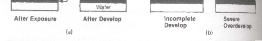
18 Line width as function of development
19 Development Process Immersion possible but same drawbacks as primer immersion. Spray, Rinse, Dry Puddle, Spray, Rinse, Dry Preferred!
20 Scum and Descumming Thin layer of resist or developer might be present on surface after rinse. Can be removed by plasma oxidation, if substrate is not damaged too severely by this
21 Eight Steps of Photolithography UV Light HMDS Resist Mask 1) Vapor prime 2) Spin coat 3) Soft bake 4) Alignment and Exposure 5) Post-exposure bake 6) Develop 7) Hard bake 8) Develop inspect
22 Hard Bake A Post-Development Thermal Bake Evaporate Remaining Solvent Improve Resist-to-Wafer Adhesion Higher Temperature (120 to 140 C) than Soft Bake

23 Hard Bake Hardening of the resist film after development. Makes it more durable for subsequent processes. Typical temperatures C and 30 min in convection oven. Other oven designs shorter duration Don t bake too hot! This will make the resist flow!
24 Photolithography Track System
25 Automated Wafer Track for Photolithography Load station Vapor prime Resist coat Develop and Rinse Edge-bead removal Transfer station Wafer stepper (Alignment/Exposure system) Wafer Transfer System Soft bake Cool plate Cool plate Hard bake
26 Photolithography Concepts Patterning process Photomask Reticle Critical dimension generations Light spectrum and wavelengths Resolution Overlay accuracy Process latitude

27 Three Basic Exposure Methods 1:1 Exposure 1:1 Exposure ~5:1 Exposure
28 Contact printing capable of high resolution but has unacceptable defect densities. May be used in Development but not manufacturing. Proximity printing cannot easily print features below a few m in line width. Used in nano-technolgy. Projection printing provides high resolution and low defect densities and dominates today. Typical projection systems use reduction optics (2X - 5X), step and repeat or step and scan. They print» 50 wafers/hour and cost $5-10M.
29 Contact lithography implementation. Normally mask is aligned with substrate and then brought into contact with substrate before exposure. Alignment Exposure
30 Contact Lithography Since illumination almost perfectly follows mask, almost perfect features can be produced regardless of contrast of resist. Contact printing produces superb images. Image quality under contact printing conditions is not a reflection of quality of resist. Disadvantages of contact printing: Contact can cause defects in resist. Contact can damage mask. Throughput limited. Contact not used in commercial production of silicon devices. However it can be used in laboratory situations as well as in special low volume production. Smallest feature sizes not easily attainable due to problems making the mask.


31 Commercial contact aligners. Suss laboratory contact aligner. Suss MA6a contact aligner. Quintel contact aligner.


32 Commercial contact aligners.continued. K-W MA1006 contact aligner Suss MA8 contact aligner
33 Contact vs. Proximity Lithography
34 Proximity lithography. In proximity lithography, the mask is held above the substrate by a fixed distance or gap. (better protection for mask) Limiting factor: Fresnel diffraction. General rule: resolution ~ (g ) 0.5 where g is gap. Derivation: Chang and Sze, ULSI Technology (McGraw Hill, 1996), p 274. Take g = 20 micron and = 0.4 micron: resolution ~ 3 micron. Since it is difficult to maintain g < 20 micron, proximity lithography is rarely used in commercial production. Some versions are widely used in research and small scale production (Suss, 250 nm wavelength).
35 Lithographic exposure and equipment. Diffraction pattern from coherently illuminated mask.
36 Projection lithography: General considerations. source Collimating optics mask Projection Lens.
37 Properties of optical lenses used in lithography. Simple lens can be characterized by diameter D and focal length, f. Source distance d 1 from lens will be focused at distance d 2 according to the relation: 1 f 1 d 1 Thus if d 1 = then d 2 = f. 1 d 2 Image will be magnified by factor m=d 2 /d 1. Could alternately define simple lens in terms of numerical aperture NA and D where NA = D/(2f). Lithographic lenses are extremely complex lenses with multiple elements to minimize aberrations resulting from several phenomena. However they can to first order be described in terms of simple lens equivalent.
38 Projection lithography: Resolution. Limitations are due to Fraunhofer diffraction. Consider the following geometry: Souce. Collection optics. Mask Projection lens: NA Image onto surface of wafer.
39 Projection lithography: General considerations. Frauenhoffer Diffraction: Resolution = k 1 / NA Minimum intensity at space is X maximum intensity. Theory: k 1 = 0.61 for optical resolution. k 1 can vary with esoteric optical systems or if response of resist is included.
Semiconductor Manufacturing Technology. Semiconductor Manufacturing Technology. Photolithography: Resist Development and Advanced Lithography
 Semiconductor Manufacturing Technology Michael Quirk & Julian Serda October 2001 by Prentice Hall Chapter 15 Photolithography: Resist Development and Advanced Lithography Eight Basic Steps of Photolithography
Photolithography I ( Part 1 )
") 1 Photolithography I ( Part 1 ) Chapter 13 : Semiconductor Manufacturing Technology by M. Quirk & J. Serda Bjørn-Ove Fimland, Department of Electronics and Telecommunication, Norwegian University of Science
1 Photolithography I ( Part 1 ) Chapter 13 : Semiconductor Manufacturing Technology by M. Quirk & J. Serda Bjørn-Ove Fimland, Department of Electronics and Telecommunication, Norwegian University of Science
Part 5-1: Lithography
 Part 5-1: Lithography Yao-Joe Yang 1 Pattern Transfer (Patterning) Types of lithography systems: Optical X-ray electron beam writer (non-traditional, no masks) Two-dimensional pattern transfer: limited
Lecture 7. Lithography and Pattern Transfer. Reading: Chapter 7
 Lecture 7 Lithography and Pattern Transfer Reading: Chapter 7 Used for Pattern transfer into oxides, metals, semiconductors. 3 types of Photoresists (PR): Lithography and Photoresists 1.) Positive: PR
Device Fabrication: Photolithography
 Device Fabrication: Photolithography 1 Objectives List the four components of the photoresist Describe the difference between +PR and PR Describe a photolithography process sequence List four alignment
Photolithography Technology and Application
 Photolithography Technology and Application Jeff Tsai Director, Graduate Institute of Electro-Optical Engineering Tatung University Art or Science? Lind width = 100 to 5 micron meter!! Resolution = ~ 3
Lecture 13 Basic Photolithography
 Lecture 13 Basic Photolithography Chapter 12 Wolf and Tauber 1/64 Announcements Homework: Homework 3 is due today, please hand them in at the front. Will be returned one week from Thursday (16 th Nov).
Chapter 6. Photolithography
 Chapter 6 Photolithography 2006/4/10 1 Objectives List the four components of the photoresist Describe the difference between +PR and PR Describe a photolithography process sequence List four alignment
Dr. Dirk Meyners Prof. Wagner. Wagner / Meyners Micro / Nanosystems Technology
 Micro/Nanosystems Technology Dr. Dirk Meyners Prof. Wagner 1 Outline - Lithography Overview - UV-Lithography - Resolution Enhancement Techniques - Electron Beam Lithography - Patterning with Focused Ion
Lithography. 3 rd. lecture: introduction. Prof. Yosi Shacham-Diamand. Fall 2004
 Lithography 3 rd lecture: introduction Prof. Yosi Shacham-Diamand Fall 2004 1 List of content Fundamental principles Characteristics parameters Exposure systems 2 Fundamental principles Aerial Image Exposure
Chapter 6 Photolithography
 Chapter 6 Photolithography Hong Xiao, Ph. D. hxiao89@hotmail.com www2.austin.cc.tx.us/hongxiao/book.htm Hong Xiao, Ph. D. www2.austin.cc.tx.us/hongxiao/book.htm 1 Objectives List the four components of
Section 2: Lithography. Jaeger Chapter 2 Litho Reader. The lithographic process
 Section 2: Lithography Jaeger Chapter 2 Litho Reader The lithographic process Photolithographic Process (a) (b) (c) (d) (e) (f) (g) Substrate covered with silicon dioxide barrier layer Positive photoresist
Section 2: Lithography. Jaeger Chapter 2 Litho Reader. EE143 Ali Javey Slide 5-1
 Section 2: Lithography Jaeger Chapter 2 Litho Reader EE143 Ali Javey Slide 5-1 The lithographic process EE143 Ali Javey Slide 5-2 Photolithographic Process (a) (b) (c) (d) (e) (f) (g) Substrate covered
Module 11: Photolithography. Lecture 14: Photolithography 4 (Continued)
") Module 11: Photolithography Lecture 14: Photolithography 4 (Continued) 1 In the previous lecture, we have discussed the utility of the three printing modes, and their relative advantages and disadvantages.
Module 11: Photolithography Lecture 14: Photolithography 4 (Continued) 1 In the previous lecture, we have discussed the utility of the three printing modes, and their relative advantages and disadvantages.
i- Line Photoresist Development: Replacement Evaluation of OiR
 i- Line Photoresist Development: Replacement Evaluation of OiR 906-12 Nishtha Bhatia High School Intern 31 July 2014 The Marvell Nanofabrication Laboratory s current i-line photoresist, OiR 897-10i, has
EE 143 Microfabrication Technology Fall 2014
 EE 143 Microfabrication Technology Fall 2014 Prof. Clark T.-C. Nguyen Dept. of Electrical Engineering & Computer Sciences University of California at Berkeley Berkeley, CA 94720 EE 143: Microfabrication
MICRO AND NANOPROCESSING TECHNOLOGIES
 MICRO AND NANOPROCESSING TECHNOLOGIES LECTURE 4 Optical lithography Concepts and processes Lithography systems Fundamental limitations and other issues Photoresists Photolithography process Process parameter
Section 2: Lithography. Jaeger Chapter 2. EE143 Ali Javey Slide 5-1
 Section 2: Lithography Jaeger Chapter 2 EE143 Ali Javey Slide 5-1 The lithographic process EE143 Ali Javey Slide 5-2 Photolithographic Process (a) (b) (c) (d) (e) (f) (g) Substrate covered with silicon
Photolithography II ( Part 2 )
") 1 Photolithography II ( Part 2 ) Chapter 14 : Semiconductor Manufacturing Technology by M. Quirk & J. Serda Saroj Kumar Patra, Department of Electronics and Telecommunication, Norwegian University of Science
1 Photolithography II ( Part 2 ) Chapter 14 : Semiconductor Manufacturing Technology by M. Quirk & J. Serda Saroj Kumar Patra, Department of Electronics and Telecommunication, Norwegian University of Science
PHGN/CHEN/MLGN 435/535: Interdisciplinary Silicon Processing Laboratory. Simple Si solar Cell!
 Where were we? Simple Si solar Cell! Two Levels of Masks - photoresist, alignment Etch and oxidation to isolate thermal oxide, deposited oxide, wet etching, dry etching, isolation schemes Doping - diffusion/ion
Semiconductor Technology
 Semiconductor Technology from A to Z + - x 1 0 x Photolithographie www.halbleiter.org Contents Contents List of Figures III 1 Photolithographie 1 1.1 Exposure and resist coating..........................
EE143 Fall 2016 Microfabrication Technologies. Lecture 3: Lithography Reading: Jaeger, Chap. 2
 EE143 Fall 2016 Microfabrication Technologies Lecture 3: Lithography Reading: Jaeger, Chap. 2 Prof. Ming C. Wu wu@eecs.berkeley.edu 511 Sutardja Dai Hall (SDH) 1-1 The lithographic process 1-2 1 Photolithographic
Lithography Is the Designer s Brush. Lithography is indispensible for defining locations and configurations of circuit elements/functions.
 Lithography 1 Lithography Is the Designer s Brush Lithography is indispensible for defining locations and configurations of circuit elements/functions. 2 ITRS 2007 The major challenge in litho: CD, CD
ECSE 6300 IC Fabrication Laboratory Lecture 3 Photolithography. Lecture Outline
 ECSE 6300 IC Fabrication Laboratory Lecture 3 Photolithography Prof. James J. Q. Lu Bldg. CII, Rooms 6229 Rensselaer Polytechnic Institute Troy, NY 12180 Tel. (518)276 2909 e mails: luj@rpi.edu http://www.ecse.rpi.edu/courses/s18/ecse
Outline. 1 Introduction. 2 Basic IC fabrication processes. 3 Fabrication techniques for MEMS. 4 Applications. 5 Mechanics issues on MEMS MDL NTHU
 Outline 1 Introduction 2 Basic IC fabrication processes 3 Fabrication techniques for MEMS 4 Applications 5 Mechanics issues on MEMS 2.2 Lithography Reading: Runyan Chap. 5, or 莊達人 Chap. 7, or Wolf and
KMPR 1010 Process for Glass Wafers
 KMPR 1010 Process for Glass Wafers KMPR 1010 Steps Protocol Step System Condition Note Plasma Cleaning PVA Tepla Ion 10 5 mins Run OmniCoat Receipt Dehydration Any Heat Plate 150 C, 5 mins HMDS Coating
T in sec, I in W/cm 2, E in J/cm 2
 Exposures from Mask Aligner into Resist Mask aligner images created by shadowing from mask into resist Soft contact and Proximity good for 3 micron structures Vacuum Hard Contact: no shadow effects at
T in sec, I in W/cm 2, E in J/cm 2
 Exposures from Mask Aligner into Resist Mask aligner images created by shadowing from mask into resist Soft contact and Proximity good for 3 micron structures Vacuum Hard Contact: no shadow effects at
2 Integrated Circuit Manufacturing:
 2 Integrated Circuit Manufacturing: A Technology Resource 2 IC MANUFACTURING TECHNOLOGIES While the integrated circuit drives the packaging and assembly, the IC manufacturing process, and associated methodologies,
CMOS Digital Integrated Circuits Lec 2 Fabrication of MOSFETs
 CMOS Digital Integrated Circuits Lec 2 Fabrication of MOSFETs 1 CMOS Digital Integrated Circuits 3 rd Edition Categories of Materials Materials can be categorized into three main groups regarding their
Optical Requirements
 Optical Requirements Transmission vs. Film Thickness A pellicle needs a good light transmission and long term transmission stability. Transmission depends on the film thickness, film material and any anti-reflective
FABRICATION OF CMOS INTEGRATED CIRCUITS. Dr. Mohammed M. Farag
 FABRICATION OF CMOS INTEGRATED CIRCUITS Dr. Mohammed M. Farag Outline Overview of CMOS Fabrication Processes The CMOS Fabrication Process Flow Design Rules Reference: Uyemura, John P. "Introduction to
Process Optimization
 Process Optimization Process Flow for non-critical layer optimization START Find the swing curve for the desired resist thickness. Determine the resist thickness (spin speed) from the swing curve and find
Photolithography. References: Introduction to Microlithography Thompson, Willson & Bowder, 1994
 Photolithography References: Introduction to Microlithography Thompson, Willson & Bowder, 1994 Microlithography, Science and Technology Sheats & Smith, 1998 Any other Microlithography or Photolithography
College of Engineering Department of Electrical Engineering and Computer Sciences University of California, Berkeley
 College of Engineering Department of Electrical Engineering and Below are your weekly quizzes. You should print out a copy of the quiz and complete it before your lab section. Bring in the completed quiz
William Reiniach 5th Year Microelectronic Engineering Student Rochester Institute of Technology
 DEVELOPMENT OF A PHOTOSENSITIVE POLYIMIDE PROCESS William Reiniach 5th Year Microelectronic Engineering Student Rochester Institute of Technology 1~BS TRACT A six step lithographic process has been developed
AZ 1512 RESIST PHOTOLITHOGRAPHY
 AZ 1512 RESIST PHOTOLITHOGRAPHY STANDARD OPERATIONAL PROCEDURE Faculty Supervisor: Prof. R. Bruce Darling Students: Katherine Lugo Danling Wang Department of Electrical Engineering Spring, 2009 TABLE OF
5. Lithography. 1. photolithography intro: overall, clean room 2. principle 3. tools 4. pattern transfer 5. resolution 6. next-gen
 5. Lithography 1. photolithography intro: overall, clean room 2. principle 3. tools 4. pattern transfer 5. resolution 6. next-gen References: Semiconductor Devices: Physics and Technology. 2 nd Ed. SM
Module - 2 Lecture - 13 Lithography I
 Nano Structured Materials-Synthesis, Properties, Self Assembly and Applications Prof. Ashok. K.Ganguli Department of Chemistry Indian Institute of Technology, Delhi Module - 2 Lecture - 13 Lithography
MICROCHIP MANUFACTURING by S. Wolf
 MICROCHIP MANUFACTURING by S. Wolf Chapter 19 LITHOGRAPHY II: IMAGE-FORMATION and OPTICAL HARDWARE 2004 by LATTICE PRESS CHAPTER 19 - CONTENTS Preliminaries: Wave- Motion & The Behavior of Light Resolution
DOE Project: Resist Characterization
 DOE Project: Resist Characterization GOAL To achieve high resolution and adequate throughput, a photoresist must possess relatively high contrast and sensitivity to exposing radiation. The objective of
Chapter 2 Silicon Planar Processing and Photolithography
 Chapter 2 Silicon Planar Processing and Photolithography The success of the electronics industry has been due in large part to advances in silicon integrated circuit (IC) technology based on planar processing,
EE-527: MicroFabrication
 EE-57: MicroFabrication Exposure and Imaging Photons white light Hg arc lamp filtered Hg arc lamp excimer laser x-rays from synchrotron Electrons Ions Exposure Sources focused electron beam direct write
Photolithography Module
 Electronics Workforce Development System Photolithography Module Introduction Photolithography Module This module will teach students the different types of microlithographic systems being used today,
Technology for the MEMS processing and testing environment. SUSS MicroTec AG Dr. Hans-Georg Kapitza
 Technology for the MEMS processing and testing environment SUSS MicroTec AG Dr. Hans-Georg Kapitza 1 SUSS MicroTec Industrial Group Founded 1949 as Karl Süss KG GmbH&Co. in Garching/ Munich San Jose Waterbury
ADVANCED MASK MAKING AT RIT. David P. Kanen 5th Year Microelectronic Engineer Student Rochester Institute of Technology ABSTRACT
 ADVANCED MASK MAKING AT RIT David P. Kanen 5th Year Microelectronic Engineer Student Rochester Institute of Technology ABSTRACT This project involved the definition of the steps necessary to generate a
Lecture 5. Optical Lithography
 Lecture 5 Optical Lithography Intro For most of microfabrication purposes the process (e.g. additive, subtractive or implantation) has to be applied selectively to particular areas of the wafer: patterning
T in sec, I in W/cm 2, E in J/cm 2
 Exposures from Mask Aligner into Resist Mask aligner images created by shadowing from mask into resist Soft contact and Proximity good for 3 micron structures Vacuum Hard Contact: no shadow effects at
Optolith 2D Lithography Simulator
 2D Lithography Simulator Advanced 2D Optical Lithography Simulator 4/13/05 Introduction is a powerful non-planar 2D lithography simulator that models all aspects of modern deep sub-micron lithography It
Micro/Nanolithography
 Dale E. Ewbank dale.ewbank@rit.edu unl081413_microe.ppt 2013 Dale E. Ewbank page 1 OUTLINE Masks Optical Lithography Photoresist Sensitivity Processing Exposure Tools Advanced Processes page 2 MICROLITHOGRAPHY
Microlithography. Dale E. Ewbank ul ppt. Microlithography Dale E. Ewbank page 1
 Dale E. Ewbank dale.ewbank@rit.edu ul012014.ppt 2014 Dale E. Ewbank page 1 OUTLINE Masks Optical Lithography Photoresist Sensitivity Processing Exposure Tools Advanced Processes page 2 MICROLITHOGRAPHY
Transistor was first invented by William.B.Shockley, Walter Brattain and John Bardeen of Bell Labratories. In 1961, first IC was introduced.
 Unit 1 Basic MOS Technology Transistor was first invented by William.B.Shockley, Walter Brattain and John Bardeen of Bell Labratories. In 1961, first IC was introduced. Levels of Integration:- i) SSI:-
MeRck. AZ nlof technical datasheet. Negative Tone Photoresist for Single Layer Lift-Off APPLICATION TYPICAL PROCESS. SPIN CURVE (150MM Silicon)
") MeRck technical datasheet AZ nlof 5510 Negative Tone Photoresist for Single Layer Lift-Off APPLICATION AZ nlof 5510 i-line photoresist is engineered to simplify the historically complex image reversal
MeRck technical datasheet AZ nlof 5510 Negative Tone Photoresist for Single Layer Lift-Off APPLICATION AZ nlof 5510 i-line photoresist is engineered to simplify the historically complex image reversal
Supporting Information. High-Resolution Organic Light Emitting Diodes Patterned via Contact Printing
 Supporting Information High-Resolution Organic Light Emitting Diodes Patterned via Contact Printing Jinhai Li, Lisong Xu, Ching W. Tang and Alexander A. Shestopalov* Department of Chemical Engineering,
Applications of Maskless Lithography for the Production of Large Area Substrates Using the SF-100 ELITE. Jay Sasserath, PhD
 Applications of Maskless Lithography for the Production of Large Area Substrates Using the SF-100 ELITE Executive Summary Jay Sasserath, PhD Intelligent Micro Patterning LLC St. Petersburg, Florida Processing
MeRck. nlof 2000 Series. technical datasheet. Negative Tone Photoresists for Single Layer Lift-Off APPLICATION TYPICAL PROCESS
 MeRck technical datasheet AZ Negative Tone Photoresists for Single Layer Lift-Off APPLICATION AZ i-line photoresists are engineered to simplify the historically complex image reversal and multilayer lift-off
Lithography. Development of High-Quality Attenuated Phase-Shift Masks
 Lithography S P E C I A L Development of High-Quality Attenuated Phase-Shift Masks by Toshihiro Ii and Masao Otaki, Toppan Printing Co., Ltd. Along with the year-by-year acceleration of semiconductor device
State-of-the-art device fabrication techniques
 State-of-the-art device fabrication techniques! Standard Photo-lithography and e-beam lithography! Advanced lithography techniques used in semiconductor industry Deposition: Thermal evaporation, e-gun
THE USE OF A CONTRAST ENHANCEMENT LAYER TO EXTEND THE PRACTICAL RESOLUTION LIMITS OF OPTICAL LITHOGRAPHIC SYSTEMS
 THE USE OF A CONTRAST ENHANCEMENT LAYER TO EXTEND THE PRACTICAL RESOLUTION LIMITS OF OPTICAL LITHOGRAPHIC SYSTEMS Daniel R. Sutton 5th Year Microelectronic Engineering Student Rochester Institute of Technology
Microlens formation using heavily dyed photoresist in a single step
 Microlens formation using heavily dyed photoresist in a single step Chris Cox, Curtis Planje, Nick Brakensiek, Zhimin Zhu, Jonathan Mayo Brewer Science, Inc., 2401 Brewer Drive, Rolla, MO 65401, USA ABSTRACT
Module 11: Photolithography. Lecture11: Photolithography - I
 Module 11: Photolithography Lecture11: Photolithography - I 1 11.0 Photolithography Fundamentals We will all agree that incredible progress is happening in the filed of electronics and computers. For example,
Contrast Enhancement Materials CEM 365HR
 INTRODUCTION In 1989 Shin-Etsu Chemical acquired MicroSi, Inc. including their Contrast Enhancement Material (CEM) technology business*. A concentrated effort in the technology advancement of a CEM led
CHAPTER 2 Principle and Design
 CHAPTER 2 Principle and Design The binary and gray-scale microlens will be designed and fabricated. Silicon nitride and photoresist will be taken as the material of the microlens in this thesis. The design
Notes. (Subject Code: 7EC5)
") COMPUCOM INSTITUTE OF TECHNOLOGY & MANAGEMENT, JAIPUR (DEPARTMENT OF ELECTRONICS & COMMUNICATION) Notes VLSI DESIGN NOTES (Subject Code: 7EC5) Prepared By: MANVENDRA SINGH Class: B. Tech. IV Year, VII
COMPUCOM INSTITUTE OF TECHNOLOGY & MANAGEMENT, JAIPUR (DEPARTMENT OF ELECTRONICS & COMMUNICATION) Notes VLSI DESIGN NOTES (Subject Code: 7EC5) Prepared By: MANVENDRA SINGH Class: B. Tech. IV Year, VII
Discovering Electrical & Computer Engineering. Carmen S. Menoni Professor Week 3 armain.
 Discovering Electrical & Computer Engineering Carmen S. Menoni Professor Week 3 http://www.engr.colostate.edu/ece103/semin armain.html TOP TECH 2012 SPECIAL REPORT IEEE SPECTRUM PAGE 28, JANUARY 2012 P.E.
(ksaligner & quintel resolution)
") Process [4.10] (ksaligner & quintel resolution) 1.0 Process Summary 1.1 Since Karl Suss ksaligner is heavily used and Quintel aligner is not, nanolab decided to compare the 2 micron line resolution from
Process [4.10] (ksaligner & quintel resolution) 1.0 Process Summary 1.1 Since Karl Suss ksaligner is heavily used and Quintel aligner is not, nanolab decided to compare the 2 micron line resolution from
+ Preferred material for tool O Acceptable material for tool X Unacceptable material for tool
 Contact Aligners (HTG, ABM, EV620) GCA 5X g-line Stepper GCA i-line Steppers (GCA 10X, AS200) Shipley 1800 Series (1805, 1813, 1818, 1827) + + X AZ nlof 2000 O X + AZ4903 + + X OiR 620-7i X X + OiR 897-12i
MICROBUMP CREATION SYSTEM FOR ADVANCED PACKAGING APPLICATIONS
 MICROBUMP CREATION SYSTEM FOR ADVANCED PACKAGING APPLICATIONS Andrew Ahr, EKC Technology, & Chester E. Balut, DuPont Electronic Technologies Alan Huffman, RTI International Abstract Today, the electronics
32nm High-K/Metal Gate Version Including 2nd Generation Intel Core processor family
 From Sand to Silicon Making of a Chip Illustrations 32nm High-K/Metal Gate Version Including 2nd Generation Intel Core processor family April 2011 1 The illustrations on the following foils are low resolution
A review on contemporary practices in Lithography
 IOSR Journal of Applied Chemistry (IOSR-JAC) e-issn: 2278-5736.Volume 7, Issue 4 Ver. II. (Apr. 2014), PP 27-31 A review on contemporary practices in Lithography Perna Kishor Krishna, Mantha Anil Srimanth,
Micro- and Nano-Technology... for Optics
 Micro- and Nano-Technology...... for Optics 3.2 Lithography U.D. Zeitner Fraunhofer Institut für Angewandte Optik und Feinmechanik Jena Printing on Stones Map of Munich Stone Print Shadow Printing Photomask
A process for, and optical performance of, a low cost Wire Grid Polarizer
 1.0 Introduction A process for, and optical performance of, a low cost Wire Grid Polarizer M.P.C.Watts, M. Little, E. Egan, A. Hochbaum, Chad Jones, S. Stephansen Agoura Technology Low angle shadowed deposition
Optical Issues in Photolithography
 OpenStax-CNX module: m25448 1 Optical Issues in Photolithography Andrew R. Barron This work is produced by OpenStax-CNX and licensed under the Creative Commons Attribution License 3.0 note: This module
Topic 3. CMOS Fabrication Process
 Topic 3 CMOS Fabrication Process Peter Cheung Department of Electrical & Electronic Engineering Imperial College London URL: www.ee.ic.ac.uk/pcheung/ E-mail: p.cheung@ic.ac.uk Lecture 3-1 Layout of a Inverter
University of California, Berkeley Department of Mechanical Engineering. ME 290R Topics in Manufacturing, Fall 2014: Lithography
 University of California, Berkeley Department of Mechanical Engineering ME 290R Topics in Manufacturing, Fall 2014: Lithography Class meetings: TuTh 3.30 5pm in 1165 Etcheverry Tentative class schedule
Fabrication Methodology of microlenses for stereoscopic imagers using standard CMOS process. R. P. Rocha, J. P. Carmo, and J. H.
 Fabrication Methodology of microlenses for stereoscopic imagers using standard CMOS process R. P. Rocha, J. P. Carmo, and J. H. Correia Department of Industrial Electronics, University of Minho, Campus
Micro- and Nano-Technology... for Optics
 Micro- and Nano-Technology...... for Optics 3.2 Lithography U.D. Zeitner Fraunhofer Institut für Angewandte Optik und Feinmechanik Jena Printing on Stones Map of Munich Stone Print Contact Printing light
immersion optics Immersion Lithography with ASML HydroLith TWINSCAN System Modifications for Immersion Lithography by Bob Streefkerk
 immersion optics Immersion Lithography with ASML HydroLith by Bob Streefkerk For more than 25 years, many in the semiconductor industry have predicted the end of optical lithography. Recent developments,
Contrast Enhancement Materials CEM 365iS
 INTRODUCTION In 1989 Shin-Etsu Chemical acquired MicroSi, Inc. and the Contrast Enhancement Material (CEM) technology business from General Electric including a series of patents and technologies*. A concentrated
Integrated Focusing Photoresist Microlenses on AlGaAs Top-Emitting VCSELs
 Integrated Focusing Photoresist Microlenses on AlGaAs Top-Emitting VCSELs Andrea Kroner We present 85 nm wavelength top-emitting vertical-cavity surface-emitting lasers (VCSELs) with integrated photoresist
The End of Thresholds: Subwavelength Optical Linewidth Measurement Using the Flux-Area Technique
 The End of Thresholds: Subwavelength Optical Linewidth Measurement Using the Flux-Area Technique Peter Fiekowsky Automated Visual Inspection, Los Altos, California ABSTRACT The patented Flux-Area technique
EG2605 Undergraduate Research Opportunities Program. Large Scale Nano Fabrication via Proton Lithography Using Metallic Stencils
 EG2605 Undergraduate Research Opportunities Program Large Scale Nano Fabrication via Proton Lithography Using Metallic Stencils Tan Chuan Fu 1, Jeroen Anton van Kan 2, Pattabiraman Santhana Raman 2, Yao
Lecture 8. Microlithography
 Lecture 8 Microlithography Lithography Introduction Process Flow Wafer Exposure Systems Masks Resists State of the Art Lithography Next Generation Lithography (NGL) Recommended videos: http://www.youtube.com/user/asmlcompany#p/search/1/jh6urfqt_d4
Semiconductor Physics and Devices
 Metal-Semiconductor and Semiconductor Heterojunctions The Metal-Oxide-Semiconductor Field-Effect Transistor (MOSFET) is one of two major types of transistors. The MOSFET is used in digital circuit, because
Institute of Solid State Physics. Technische Universität Graz. Lithography. Peter Hadley
 Technische Universität Graz Institute of Solid State Physics Lithography Peter Hadley http://www.cleanroom.byu.edu/virtual_cleanroom.parts/lithography.html http://www.cleanroom.byu.edu/su8.phtml Spin coater
Opto-Mechanical Equipment of KBTEM: Present Day and the Future
 KBTEM JSC, Minsk, Belarus Opto-Mechanical Equipment of KBTEM: Present Day and the Future Quality Management System Certificate ISO-9001 since 2001 SPIE Member since 2003 www.kb-omo.by Dr. S.Avakaw SEMI
Low-power carbon nanotube-based integrated circuits that can be transferred to biological surfaces
 SUPPLEMENTARY INFORMATION Articles https://doi.org/10.1038/s41928-018-0056-6 In the format provided by the authors and unedited. Low-power carbon nanotube-based integrated circuits that can be transferred
From Sand to Silicon Making of a Chip Illustrations May 2009
 From Sand to Silicon Making of a Chip Illustrations May 2009 1 The illustrations on the following foils are low resolution images that visually support the explanations of the individual steps. For publishing
Layout of a Inverter. Topic 3. CMOS Fabrication Process. The CMOS Process - photolithography (2) The CMOS Process - photolithography (1) v o.
 The CMOS Process - photolithography (1) v o.") Layout of a Inverter Topic 3 CMOS Fabrication Process V DD Q p Peter Cheung Department of Electrical & Electronic Engineering Imperial College London v i v o Q n URL: www.ee.ic.ac.uk/pcheung/ E-mail: p.cheung@ic.ac.uk
Layout of a Inverter Topic 3 CMOS Fabrication Process V DD Q p Peter Cheung Department of Electrical & Electronic Engineering Imperial College London v i v o Q n URL: www.ee.ic.ac.uk/pcheung/ E-mail: p.cheung@ic.ac.uk
Clean Room Technology Optical Lithography. Lithography I. takenfrombdhuey
 Clean Room Technology Optical Lithography Lithography I If the automobile had followed the same development cycle as the computer, a Rolls Royce would today cost $100, get a million miles per gallon, and
MICROLITHOGRAPHY 2004
 MICROLITHOGRAPHY 2004 From Computer Aided Design (CAD) to Patterned Substrate At the CNF, a number of different options exist for producing a patterned substrate, but deciding which option is best for
Optical Lithography. Here Is Why. Burn J. Lin SPIE PRESS. Bellingham, Washington USA
 Optical Lithography Here Is Why Burn J. Lin SPIE PRESS Bellingham, Washington USA Contents Preface xiii Chapter 1 Introducing Optical Lithography /1 1.1 The Role of Lithography in Integrated Circuit Fabrication
Micro-Nanofabrication
 Zheng Cui Micro-Nanofabrication TECHNOLOGIES AND APPLICATIONS ^f**"?* ö Springer Higher Education Press -T O Table of Content Preface About the Author Chapter 1 Introduction 1 1.1 Micro-nanotechnologies
Newer process technology (since 1999) includes :
 includes :") Newer process technology (since 1999) includes : copper metalization hi-k dielectrics for gate insulators si on insulator strained silicon lo-k dielectrics for interconnects Immersion lithography for masks
Newer process technology (since 1999) includes : copper metalization hi-k dielectrics for gate insulators si on insulator strained silicon lo-k dielectrics for interconnects Immersion lithography for masks
All-Glass Gray Scale PhotoMasks Enable New Technologies. Che-Kuang (Chuck) Wu Canyon Materials, Inc.
 Wu Canyon Materials, Inc.") All-Glass Gray Scale PhotoMasks Enable New Technologies Che-Kuang (Chuck) Wu Canyon Materials, Inc. 1 Overview All-Glass Gray Scale Photomask technologies include: HEBS-glasses and LDW-glasses HEBS-glass
All-Glass Gray Scale PhotoMasks Enable New Technologies Che-Kuang (Chuck) Wu Canyon Materials, Inc. 1 Overview All-Glass Gray Scale Photomask technologies include: HEBS-glasses and LDW-glasses HEBS-glass
Design Rules for Silicon Photonics Prototyping
 Design Rules for licon Photonics Prototyping Version 1 (released February 2008) Introduction IME s Photonics Prototyping Service offers 248nm lithography based fabrication technology for passive licon-on-insulator
Figure 7 Dynamic range expansion of Shack- Hartmann sensor using a spatial-light modulator
 Figure 4 Advantage of having smaller focal spot on CCD with super-fine pixels: Larger focal point compromises the sensitivity, spatial resolution, and accuracy. Figure 1 Typical microlens array for Shack-Hartmann
EE141-Fall 2009 Digital Integrated Circuits
 EE141-Fall 2009 Digital Integrated Circuits Lecture 2 Integrated Circuit Basics: Manufacturing and Cost 1 1 Administrative Stuff Discussions start this Friday We have a third GSI Richie Przybyla, rjp@eecs
Innovative Mask Aligner Lithography for MEMS and Packaging
 Innovative Mask Aligner Lithography for MEMS and Packaging Dr. Reinhard Voelkel CEO SUSS MicroOptics SA September 9 th, 2010 1 SUSS Micro-Optics SUSS MicroOptics is a leading supplier for high-quality
Chapter 3 Fabrication
 Chapter 3 Fabrication The total structure of MO pick-up contains four parts: 1. A sub-micro aperture underneath the SIL The sub-micro aperture is used to limit the final spot size from 300nm to 600nm for