R&D Status and Key Technical and Implementation Challenges for EUV HVM
|
|
|
- Brian Garrison
- 6 years ago
- Views:
Transcription
1 R&D Status and Key Technical and Implementation Challenges for EUV HVM Sam Intel Corporation
2 Agenda Requirements by Process Node EUV Technology Status and Gaps Photoresists Tools Reticles Summary 2

3 Moore s Law at Intel The trend is expected to continue 3

4 Transistor Density Trend 4


5 On-Time 2 Year Cycle 130 nm 90 nm 65 nm 45 nm 32 nm 22 nm forecast 2011 forecast In Development 291 Mb SRAM 2 ND gen. HK+MG 5


6 Paths to Feature Size Scaling d = k 1 λ NA NA = 0.93 λ= 193nm Increase NA Enable reduced pitches through process options (like double patterning) Reduce Wavelength k k 1 < 0.3 tends to have 0.25 manufacturability issues Feature Size (nm) 6
7 Lithography Transitions If current lithography is capable of delivering a manufacturable process, use it If not: If new lithography technology is ready, manufacturable and cost-effective, use it (increase NA, reduce λ) If not: need to make alternative decisions to enable scaling without litho improvements (operate more effectively at lower k 1 ) Managing litho transitions is key! Requires significant planning 7
8 1.2 ArF Pitch Division vs. EUV NA ArF DP 1.35NA ArF EUV k NA ArF?? 0.3 k 1 = /2 Pitch (nm)? 45nm node 80nm HP 07 HVM Dry 32nm node 56nm HP 09 HVM Immersion 22nm node ~40nm HP 11 HVM Immersion 15nm node 26-30nm HP 13 HVM ArF PD/ EUV 11nm node 18-22nm HP 15 HVM ArF PD/ EUV 8
9 Patterning Choices for 15nm and 11nm ArF Pitch Division EUV Advantages: Known technology Well-established infrastructure Mature photoresist and tooling Disadvantages: Complex process flow Very expensive Complicated DRs Advantages: Single exposure Simpler DRs Disadvantages: Unknown technology Infrastructure needs to be developed Immature photoresist, tooling 9

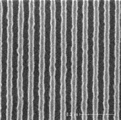
10 ArF Pitch Division Double Patterning Pitch Division (DPPD) Spacer Based Pitch Division (SBPD) Half Pitch (nm) NA ArF PD gains significant resolution at the expense of process complexity 10


11 λ Scaling The Case for EUV 28nm ArF DP EUV HP k
12 EUV HVM Key Requirements Stable hardware Scanner platform Optics Overlay/stage System (vacuum) Source Reliability and uptime Power Photoresist that meets requirements Resolution, sensitivity, LWR Etch interactions Reticles Defectivity Infrastructure (cleans, inspections, handling) Success of EUV in HVM will depend on progress on all these fronts 12
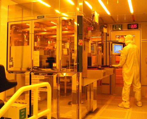
13 Exposure Tooling 13
14 External EUV Exposure Tooling Nikon EUV1 alpha tool 0.25NA full field scanner Currently installed at Nikon and SELETE ASML Alpha Demo Tool (ADT) 0.25NA full field scanner Currently installed at IMEC and SEMATECH Intel Internal MET small-field exposure tool Target application is resist development 14


15 EUV HVM Exposure Tooling Development ASML ADT printed wafer Nikon EUV1 printed wafer EUV Source Suppliers are competing towards HVM tool development Cymer beta source Philips beta source 15


16 Nikon EUV1 Tool Field Size 26 x 33 mm 2 NA and Magnification 0.25, x1/4 Illumination Sigma Overlay Adjustable 10 nm WFE 0.4 nm RMS (average) mm Min. 0.3nm RMS ~ Max. 0.5nm RMS 16


 28")
 5.33 5.")
17 Nikon EUV Tool Data Lines (Static) Ultimate Resolution 26nm HP LWR 7.05nm Esize 17.8mJ/cm 2 32/64nm Line Ends HP (nm) LWR (nm) DOF (nm) 140 >210 >210 >280 17


 6.")
")
18 Nikon EUV Tool Data Trenches (Static) Ultimate Resolution 31nm HP LWR 7.22nm Esize 16.2mJ/cm 2 32/64nm Line End Trench HP (nm) LWR (nm) DOF (nm) >100 >140 >160 >180 18

19 ASML Alpha Demo Tool (ADT) 19

20 ADT Patterning Results 20

21 ADT Overlay Stability Data 21

22 Cymer LPP EUV Source Photo Courtesy of Nigel Farrar, Cymer, Inc. 22

23 Cymer EUV Source 23

24 Philips DPP EUV Source 24
25 Photoresists 25
 0.")

26 0.3NA capability 600 x 600 µm field Low flare (3-6%) Intel MET Source: (XTREME DPF Source) 0.5mm x 2mm (FWHM) 35W EUV in 2π New EUV collector installed New outer shell extended σ outer from 0.55 to 0.65, 22nm HP resolution with quadrupole illumination First step in preparation for 0.5 NA MET projection optics (2010) that will enable ~10nm HP resolution 26

27 Intel MET Status Uptime average: 67% in 07, 85% in 08, 63% through WW22 in 09 Continuous improvement in output efficiency 13J/cm 2 /day currently On track to deliver more dose in 2009 than in 2008 Improved resolution and expanded process window Long term upgrade path defined down to ~10nm HP > 250 Resists Screened in 08. Goal > 500 in 09 27


28 New MET Quad Source Enables 22nm HP Quad 0.68/ nm HP 28nm HP 26nm HP 24nm HP 22nm HP 20nm HP 28
 ::")


29 Berkeley ALS-MET (Rotated Dipole) :: Champion RLS Summary for hp Resist D Esize = mj Min LWR = 4.8 nm UR ~ 28 nm HP SMT01 Esize = mj Min LWR = 6.2 nm UR ~ 24 nm HP Resist E Esize = 9.95 mj Min LWR = 6.3 nm UR~ 24 nm HP Resist F Esize = 6.85 mj Min LWR = 5.3 nm UR~ 26 nm HP 22 HP 30 HP Champion CAR platforms Nominally Meeting 22nm HP R/S Targets but Failing for LWR/PC 29

30 Pattern Collapse Margin Improvement Pattern Collapse Mitigation is primary focus for 2009 Multiple approaches may be needed to address problem Modify Aspect Ratio Surface (Energy)Optimization: Hydrophobicity, Multilayer stacks Increased resist modulus, Negative Tone & Semi-organic Resists Decreased Surface Tension: Rinse agents, Organic Developers, Develop/Rinse/Spin Dry Process Optimization 30
")


 Multiple techniques may be")
31 LWR Reduction Techniques No Treatment Technique Etch/Trim Reduction (nm) Reduction (%) Etch/Trim Vapor Smoothing Hardbake Ozonation Rinse 2 40 Vapor Hardbake Ozonation Physical (Etch/Trim, Hardbake) Photoresist chemistry independent Chemical (Vapor, Ozonation, Rinse Agent) Photoresist chemistry dependent Rinse Chandhok et al, J. Vac. Sci. Technol. B, (Nov 2008) Multiple techniques may be needed to address LF & HF roughness Largest LWR Improvement Seen with Rinse Agent 31
 Power (W) Current ~20 Target 200 Improvement Required 10X Scanner Runrate Runrate (wph) Current 5 Target 100 Improvement")
32 Resist and Tooling Gaps Photospeed (mj/cm 2 ) 3σ LWR (nm) Current 10/20 3.8/6.4 Target /1.28 Improvement Required None/2X 2X/5X Source Power Photoresists (32/22nm HP) Power (W) Current ~20 Target 200 Improvement Required 10X Scanner Runrate Runrate (wph) Current 5 Target 100 Improvement Required 20X Summary: Good progress made to date Need continued work to bridge (or significantly reduce) gaps for both performance and COO 32
33 Reticles 33

34 HVM Reticle Infrastructure Requirements Reticle Requirements Mask Shop Mask Manufacturing Mask Cleaning Blank inspection Patterned inspection AIMS inspection Fab In-situ Inspection Patterned Inspection Need inspection capability in both the mask shop and the fab to ensure manufacturable operations 34


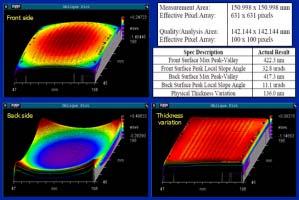

35 Intel s Mask Tool Pilot Line 1G & 2G Blank Inspection Flatness EUV Refl Film Dep 3G Actinic Blank Inspection Sorter Patterned mask inspection Mask Clean EUV AIMS 35


36 Mask Blank Yield Gap for Pilot Line and HVM Introduction Determine Defect Density Target defects/cm 18 nm is the historical defect free target However, recent data suggests only 10-20% of defects print The ultimate HVM defect density target might be nm Today: 1 defect/cm Gap to Pilot: > 25x Gap to HVM: >100x Pilot Line Yield defects/cm 2 Today 10-20% of defects print HVM Pilot HVM Yield Data from Sematech 36
37 Jan-06 Jan-07 Jan-08 Jan-09 Jan-10 Jan-11 Jan-12 Jan-13 Jan-14 Defect counts 1.E+04 1.E+03 1.E+02 1.E+01 1.E+00 Mask Blank Defect Trends 80nm 1G inspection tool 45nm 50nm 45nm 2G tool 35nm 35nm 80nm defect size 50nm defect size RM-for blank need by 2012 RM-for blank need by G Actinic Inspection 30nm 25nm 3G tool 25nm 20nm Actual Needed Metrology Tool Gap Limits HVM Insertion! 37

38 New Blank Defect Inspection Capability M1350 M7360 Blank inspection tool G1 (M1350) G2 (M7360) Laser source λ 488 nm 266 nm > 98% capture rate 2004-Q2 08 Q3 08 Q1 09 Def. on quartz substrate 70 nm 45 nm 35 nm Def. on ML blank 80 nm 50 nm 40 nm 2 nd -gen mask blank inspection tool successfully installed in June Inspectability will be further extended with spatial filter upgrade in Q4 Moving toward ultimate 25nm inspection requirement for
39 AIMS and Patterned Defect Inspections AIMS: Industry requirement: 22nm hp+ defect repair verification with scanner conditions Strategy for 2013 HVM: HVM tool requires commercial partner, but market is small Consortium model attempts underway July summit Patterned: Industry Requirement: Patterned defect inspection at 22nm HP KLA6XX will achieve 32nm and some 22nm HP performance Strategy for 2013 HVM: Market is sizeable and tool cost significant Suppliers unwilling to bear $250M NRE cost alone July summit SEMATECH contribution will be to broker funding model 39
![HVM Pilot Development EUV Mask Inspection Tools Summary Defect Size [nm] 51 67 41 35 20 15 Substrate 53 40 25 20 15 Blank Substrate & Blank Lasertec M1350 (1st Generation) M1350 & M7360 @ SEMATECH](/docs-images/77/74888494/images/40-1.jpg "Lasertec M7360 (2nd Generation) 2.5 Generation Substrate Inspection Tool (2.")
40 HVM Pilot Development EUV Mask Inspection Tools Summary Defect Size [nm] Substrate Blank Substrate & Blank Lasertec M1350 (1st Generation) M1350 & SEMATECH Lasertec M7360 (2nd Generation) 2.5 Generation Substrate Inspection Tool (2.5G) (Supplier TBD) (can also be used for destructive blank inspection) Table from Sematech SEMATECH Berkeley AIT Selete MIRAI 3 rd Generation Blank Inspection Bridge Tool (3G ) (Supplier TBD) Commercial 3G Inspection Tool (Supplier TBD) ABC = Existing Tools AIMS & Patterned SEMATECH Berkeley AIT 88 nm mask CD resolution Key for defect printability understanding SEMATECH Berkeley AIT2 60 nm mask CD resolution AIMS Bridge tool Commercial AIMS Tool (Supplier TBD) KLA 5XX KLA 6XX Actinic Patterned Inspection (Supplier TBD) = Actinic Inspection Tools 40

 shows reticle protection down to 0.")
41 Particle-free Reticle Handling Progress spod Carrier He, et al. Proc. SPIE 6921, 69211Z (March 21, 2008) E152 standard compliant prototype (spod) shows reticle protection down to 0.1 added particles per nm. with Inner Pod Exposed 41


42 EUV Pellicle Demonstration Hexagonal Ni mesh + Si membrane high risk/cost backup project full size pellicle demonstrated uniformity impact studies underway varying standoff height and mesh size 42
43 In-situ Inspection Need to verify reticle cleanliness AFTER loading into scanner and BEFORE printing wafers Repeater concern is serious due to lack of pellicles ArF scanners have in-situ reticle inspection capability Not having in-situ capability would require printing of defect look-ahead wafers Manageable in development and perhaps in pilot line mode Unacceptable for HVM Need focus from tool vendors to have capability avaialable in HVM tooling platforms 43
44 Reticle Technical and Infrastructure Gaps Current reticle defectivity gap is about X Need continuous improvement Relaxation of flatness spec might help bridge gap Inspection gaps Actinic blank inspection Patterned defect inspection spec vs. actual In-situ inspection AIMs inspection SEMATECH is adopting a bridge tool solution for actinic blank and AIMS inspection so that some capability will be available for pilot line in 2011 Production actinic inspection, AIMS, and patterned inspection will require industry-wide funding (July workshop) 44
45 Summing Up 45
46 HVM Gaps - Overall Full field production scanner Suppliers building solutions? Estimated Cost for HVM Solution Time to HVM Solution Yes Funded 2012 Source Yes Funded 2011 Resist Yes Funded 2011 Mask Blank Multilayer Dep Actinic Blank Inspection Actinic Defect Review Mask Patterned Inspection Yes No No No Funded >50M >50M >100M ? 2013? 2013? Table from Bryan Rice, Sematech SEMATECH s EUV mask infrastructure strategy is: Obtain support from various partners (public and private) Commit most of SEMATECH s Litho budget to mask infrastructure over next four years Need industry consensus on required funding to bridge gaps 46


47 EUV Cost-Effectiveness COO! 47
 Source: http://singularity.")
48 No Exponential is forever, but we can delay forever Gordon Moore Scaling + Yield Defect Density (Log Scale) Source: Will EUV performance and COO enable us to continue to delay forever? 48
49 Conclusions Substantial progress made on resist and tooling Resists typically about 2X from goal for sensitivity/lwr Laser power about 10X from goal Overall tool runrate requires ~ 20X improvement to 100wph goal Reticle defectivity is a major concern Blank defectivity needs substantial improvement Relaxation of flatness requirement might provide some mitigation Reticle inspection capability has major gaps. Need industry funding to enable tooling to be developed in time for HVM Academic exercise is over!! EUV has moved from research to implementation mode Problems left to be solved are largely engineering in nature Need sustained focus and industry-wide commitment to solve Ultimately EUV insertion will be based on a COO decision vs. ArF 49


50
EUVL getting ready for volume introduction
 EUVL getting ready for volume introduction SEMICON West 2010 Hans Meiling, July 14, 2010 Slide 1 public Outline ASML s Lithography roadmap to support Moore s Law Progress on 0.25NA EUV systems Progress
EUVL Scanners Operational at Chipmakers. Skip Miller Semicon West 2011
 EUVL Scanners Operational at Chipmakers Skip Miller Semicon West 2011 Outline ASML s Lithography roadmap to support Moore s Law Progress on NXE:3100 (0.25NA) EUV systems Progress on NXE:3300 (0.33NA) EUV
EUV Lithography Transition from Research to Commercialization
 EUV Lithography Transition from Research to Commercialization Charles W. Gwyn and Peter J. Silverman and Intel Corporation Photomask Japan 2003 Pacifico Yokohama, Kanagawa, Japan Gwyn:PMJ:4/17/03:1 EUV
Spring of EUVL: SPIE 2012 AL EUVL Conference Review
 Spring of EUVL: SPIE 2012 AL EUVL Conference Review Vivek Bakshi, EUV Litho, Inc., Austin, Texas Monday, February 20, 2012 The SPIE Advanced Lithography EUVL Conference is usually held close to spring,
Lithography Industry Collaborations
 Accelerating the next technology revolution Lithography Industry Collaborations SOKUDO Breakfast July 13, 2011 Stefan Wurm SEMATECH Copyright 2009 SEMATECH, Inc. SEMATECH, and the SEMATECH logo are registered
Towards an affordable Cost of Ownership for EUVL. Melissa Shell Principal Engineer & Program Manager, EUVL Research Components Research October 2006
 Towards an affordable Cost of Ownership for EUVL Melissa Shell Principal Engineer & Program Manager, EUVL Research Components Research October 2006 1 Robert Bristol Heidi Cao Manish Chandhok Michael Leeson
2009 International Workshop on EUV Lithography
 Contents Introduction Absorber Stack Optimization Non-flatness Correction Blank Defect and Its Mitigation Wafer Printing Inspection Actinic Metrology Cleaning and Repair Status Remaining Issues in EUV
EUV: Status and Challenges Ahead International Workshop on EUVL, Maui 2010
 EUV: Status and Challenges Ahead International Workshop on EUVL, Maui 2010 Jos Benschop Public Agenda Roadmap Status Challenges Summary & conclusion Slide 2 Public Resolution (half pitch) "Shrink" [nm]
TSMC Property. EUV Lithography. The March toward HVM. Anthony Yen. 9 September TSMC, Ltd
 EUV Lithography The March toward HVM Anthony Yen 9 September 2016 1 1 st EUV lithography setup and results, 1986 Si Stencil Mask SR W/C Multilayer Coating Optics λ=11 nm, provided by synchrotron radiation
2008 European EUVL. EUV activities the EUVL shop future plans. Rob Hartman
 2008 European EUVL EUV activities the EUVL shop future plans Rob Hartman 2007 international EUVL Symposium 28-31 October 2007 2008 international EUVL Symposium 28 Sapporo, September Japan 1 October 2008
Holistic View of Lithography for Double Patterning. Skip Miller ASML
 Holistic View of Lithography for Double Patterning Skip Miller ASML Outline Lithography Requirements ASML Holistic Lithography Solutions Conclusions Slide 2 Shrink Continues Lithography keeps adding value
Mask Technology Development in Extreme-Ultraviolet Lithography
 Mask Technology Development in Extreme-Ultraviolet Lithography Anthony Yen September 6, 2013 Projected End of Optical Lithography 2013 TSMC, Ltd 1976 1979 1982 1985 1988 1991 1994 1997 2000 2003 2007 2012
Lithography Roadmap. without immersion lithography. Node Half pitch. 248nm. 193nm. 157nm EUVL. 3-year cycle: 2-year cycle: imec 2005
 Lithography Roadmap without immersion lithography Node Half pitch 180 nm 130 nm 90 nm 65 nm 45 nm 32 nm 22 nm 250 nm 180 nm 130 nm 90 nm 65 nm 45 nm 32 nm 248nm 193nm 157nm EUVL 3-year cycle: 2-year cycle:
Discovering Electrical & Computer Engineering. Carmen S. Menoni Professor Week 3 armain.
 Discovering Electrical & Computer Engineering Carmen S. Menoni Professor Week 3 http://www.engr.colostate.edu/ece103/semin armain.html TOP TECH 2012 SPECIAL REPORT IEEE SPECTRUM PAGE 28, JANUARY 2012 P.E.
Nikon EUVL Development Progress Update
 Nikon EUVL Development Progress Update Takaharu Miura EUVL Symposium September 29, 2008 EUVL Symposium 2008 @Lake Tahoe T. Miura September 29, 2008 Slide 1 Presentation Outline 1. Nikon EUV roadmap 2.
IMEC update. A.M. Goethals. IMEC, Leuven, Belgium
 IMEC update A.M. Goethals IMEC, Leuven, Belgium Outline IMEC litho program overview ASML ADT status 1 st imaging Tool description Resist projects Screening using interference litho K LUP / Novel resist
Progress in full field EUV lithography program at IMEC
 Progress in full field EUV lithography program at IMEC A.M. Goethals*, G.F. Lorusso*, R. Jonckheere*, B. Baudemprez*, J. Hermans*, F. Iwamoto 1, B.S. Kim 2, I.S. Kim 2, A. Myers 3, A. Niroomand 4, N. Stepanenko
Optics for EUV Lithography
 Optics for EUV Lithography Dr. Sascha Migura, Carl Zeiss SMT GmbH, Oberkochen, Germany 2018 EUVL Workshop June 13 th, 2018 Berkeley, CA, USA The resolution of the optical system determines the minimum
Computational Lithography Requirements & Challenges for Mask Making. Naoya Hayashi, Dai Nippon Printing Co., Ltd
 Computational Lithography Requirements & Challenges for Mask Making Naoya Hayashi, Dai Nippon Printing Co., Ltd Contents Introduction Lithography Trends Computational lithography options More Complex OPC
EUVL: Challenges to Manufacturing Insertion
 EUVL: Challenges to Manufacturing Insertion Obert R Wood II International Workshop on EUV Lithography CXRO, LBNL, Berkeley, California 14 June 2017 EUV Critical Issues List EUV Critical Issues, as identified
EUV lithography: today and tomorrow
 EUV lithography: today and tomorrow Vadim Banine, Stuart Young, Roel Moors Dublin, October 2012 Resolution/half pitch, "Shrink" [nm] EUV DPT ArFi ArF KrF Industry roadmap towards < 10 nm resolution Lithography
UV Nanoimprint Stepper Technology: Status and Roadmap. S.V. Sreenivasan Sematech Litho Forum May 14 th, 2008
 UV Nanoimprint Stepper Technology: Status and Roadmap S.V. Sreenivasan Sematech Litho Forum May 14 th, 2008 Overview Introduction Stepper technology status: Patterning and CD Control Through Etch Alignment
Shooting for the 22nm Lithography Goal with the. Coat/Develop Track. SOKUDO Lithography Breakfast Forum 2010 July 14 (L1)
") Shooting for the 22nm Lithography Goal with the Coat/Develop Track SOKUDO Lithography Breakfast Forum 2010 July 14 (L1) Three (3) different exposure options for 22nm: Public External (L1) MAPPER Lithography
Shooting for the 22nm Lithography Goal with the Coat/Develop Track SOKUDO Lithography Breakfast Forum 2010 July 14 (L1) Three (3) different exposure options for 22nm: Public External (L1) MAPPER Lithography
Novel EUV Resist Development for Sub-14nm Half Pitch
 EUV Workshop 2015 Maui, HI P64 Novel EUV Resist Development for Sub-14nm Half Pitch Yoshi Hishiro JSR Micro Inc. EUV Workshop, June 17, 2015 1 Contents Requirement for sub-14nm HP EUV resist JSR strategy
Scope and Limit of Lithography to the End of Moore s Law
 Scope and Limit of Lithography to the End of Moore s Law Burn J. Lin tsmc, Inc. 1 What dictate the end of Moore s Law Economy Device limits Lithography limits 2 Litho Requirement of Critical Layers Logic
Light Sources for EUV Mask Metrology. Heiko Feldmann, Ulrich Müller
 Light Sources for EUV Mask Metrology Heiko Feldmann, Ulrich Müller Dublin, October 9, 2012 Agenda 1 2 3 4 Actinic Metrology in Mask Making The AIMS EUV Concept Metrology Performance Drivers and their Relation
Reliable High Power EUV Source Technology for HVM: LPP or DPP? Vivek Bakshi, Ph.D. EUV Litho, Inc.
 Reliable High Power EUV Source Technology for HVM: LPP or DPP? Vivek Bakshi, Ph.D. EUV Litho, Inc. Presentation Outline Source Technology Requirements Source Technology Performance DPP LPP Technology Trend
450mm silicon wafers specification challenges. Mike Goldstein Intel Corp.
 450mm silicon wafers specification challenges Mike Goldstein Intel Corp. Outline Background 450mm transition program 450mm silicon evolution Mechanical grade wafers (spec case study) Developmental (test)
Challenges of EUV masks and preliminary evaluation
 Challenges of EUV masks and preliminary evaluation Naoya Hayashi Electronic Device Laboratory Dai Nippon Printing Co.,Ltd. EUV Mask Workshop 2004 1 Contents Recent Lithography Options on Roadmap Challenges
Advanced Patterning Techniques for 22nm HP and beyond
 Advanced Patterning Techniques for 22nm HP and beyond An Overview IEEE LEOS (Bay Area) Yashesh A. Shroff Intel Corporation Aug 4 th, 2009 Outline The Challenge Advanced (optical) lithography overview Flavors
EUV Light Source The Path to HVM Scalability in Practice
 EUV Light Source The Path to HVM Scalability in Practice Harald Verbraak et al. (all people at XTREME) 2011 International Workshop on EUV and Soft X-ray Sources Nov. 2011 Today s Talk o LDP Technology
TWINSCAN XT:1950i Water-based immersion taken to the max Enabling fast, single-exposure lithography at sub 40 nm
 TWINSCAN XT:1950i Water-based immersion taken to the max Enabling fast, single-exposure lithography at sub 40 nm SEMICON West, San Francisco July 14-18, 2008 Slide 1 The immersion pool becomes an ocean
Holistic Lithography. Christophe Fouquet. Executive Vice President, Applications. 24 November 2014
 Holistic Lithography Christophe Fouquet Executive Vice President, Applications 24 Holistic Lithography Introduction Customer Problem: Beyond 20nm node scanner and non scanner contributions must be addressed
Status and challenges of EUV Lithography
 Status and challenges of EUV Lithography SEMICON Europa Dresden, Germany Jan-Willem van der Horst Product Manager EUV October 10 th, 2013 Slide 2 Contents Introduction NXE:3100 NXE:3300B Summary and acknowledgements
TECHNOLOGY ROADMAP 2006 UPDATE LITHOGRAPHY FOR
 INTERNATIONAL TECHNOLOGY ROADMAP FOR SEMICONDUCTORS 2006 UPDATE LITHOGRAPHY THE ITRS IS DEVISED AND INTENDED FOR TECHNOLOGY ASSESSMENT ONLY AND IS WITHOUT REGARD TO ANY COMMERCIAL CONSIDERATIONS PERTAINING
EUV Actinic Blank Inspection Tool Development
 EUV Actinic Blank Inspection Tool Development EUVL Symposium 2011 Hiroki Miyai 1, Tomohiro Suzuki 1, Kiwamu Takehisa 1, Haruhiko Kusunose 1, Takeshi Yamane 2, Tsuneo Terasawa 2, Hidehiro Watanabe 2, Soichi
EUV Substrate, Blank, and Mask Flatness Current Specifications & Issues Overview
 EUV Mask Flatness & Carrier/Loadport Workshop October 19 th 2006 - Barcelona Spain EUV Substrate, Blank, and Mask Flatness Current Specifications & Issues Overview Phil Seidel, Chris Van Peski Stefan Wurm
450mm and Moore s Law Advanced Packaging Challenges and the Impact of 3D
 450mm and Moore s Law Advanced Packaging Challenges and the Impact of 3D Doug Anberg VP, Technical Marketing Ultratech SOKUDO Lithography Breakfast Forum July 10, 2013 Agenda Next Generation Technology
EUV lithography: status, future requirements and challenges
 EUV lithography: status, future requirements and challenges EUVL Dublin Vadim Banine with the help of Rudy Peters, David Brandt, Igor Fomenkov, Maarten van Kampen, Andrei Yakunin, Vladimir Ivanov and many
Actinic Review of EUV Masks: Performance Data and Status of the AIMS TM EUV System
 Actinic Review of EUV Masks: Performance Data and Status of the AIMS TM EUV System Dirk Hellweg*, Markus Koch, Sascha Perlitz, Martin Dietzel, Renzo Capelli Carl Zeiss SMT GmbH, Rudolf-Eber-Str. 2, 73447
Imaging for the next decade
 Imaging for the next decade Martin van den Brink Executive Vice President Products & Technology IMEC Technology Forum 2009 3 June, 2009 Slide 1 Congratulations! ASML and years of making chips better Slide
Imec pushes the limits of EUV lithography single exposure for future logic and memory
 Edition March 2018 Semiconductor technology & processing Imec pushes the limits of EUV lithography single exposure for future logic and memory Imec has made considerable progress towards enabling extreme
Update on 193nm immersion exposure tool
 Update on 193nm immersion exposure tool S. Owa, H. Nagasaka, Y. Ishii Nikon Corporation O. Hirakawa and T. Yamamoto Tokyo Electron Kyushu Ltd. January 28, 2004 Litho Forum 1 What is immersion lithography?
Scaling of Semiconductor Integrated Circuits and EUV Lithography
 Scaling of Semiconductor Integrated Circuits and EUV Lithography ( 半導体集積回路の微細化と EUV リソグラフィー ) December 13, 2016 EIDEC (Emerging nano process Infrastructure Development Center, Inc.) Hidemi Ishiuchi 1 OUTLINE
State of the art EUV mask blank inspection with a Lasertec M7360 at the SEMATECH MBDC
 State of the art EUV mask blank inspection with a Lasertec M7360 at the SEMATECH MBDC Patrick Kearney a, Won-Il Cho a, Chan-Uk Jeon a, Eric Gullikson b, Anwei Jia c, Tomoya Tamura c, Atsushi Tajima c,
Process Optimization
 Process Optimization Process Flow for non-critical layer optimization START Find the swing curve for the desired resist thickness. Determine the resist thickness (spin speed) from the swing curve and find
Beyond Immersion Patterning Enablers for the Next Decade
 Beyond Immersion Patterning Enablers for the Next Decade Colin Brodsky Manager and Senior Technical Staff Member Patterning Process Development IBM Semiconductor Research & Development Center Hopewell
(Complementary E-Beam Lithography)
") Extending Optical Lithography with C E B L (Complementary E-Beam Lithography) July 13, 2011 4008 Burton Drive, Santa Clara, CA 95054 Outline Complementary Lithography E-Beam Complements Optical Multibeam
Extending Optical Lithography with C E B L (Complementary E-Beam Lithography) July 13, 2011 4008 Burton Drive, Santa Clara, CA 95054 Outline Complementary Lithography E-Beam Complements Optical Multibeam
EUV Supporting Moore s Law
 EUV Supporting Moore s Law Marcel Kemp Director Investor Relations - Europe DB 2014 TMT Conference London September 4, 2014 Forward looking statements This document contains statements relating to certain
Competitive in Mainstream Products
 Competitive in Mainstream Products Bert Koek VP, Business Unit manager 300mm Fabs Analyst Day 20 September 2005 ASML Competitive in mainstream products Introduction Market share Device layers critical
Lecture 7. Lithography and Pattern Transfer. Reading: Chapter 7
 Lecture 7 Lithography and Pattern Transfer Reading: Chapter 7 Used for Pattern transfer into oxides, metals, semiconductors. 3 types of Photoresists (PR): Lithography and Photoresists 1.) Positive: PR
Light Source Technology Advances to Support Process Stability and Performance Predictability for ArF Immersion Double Patterning
 Light Source Technology Advances to Support Process Stability and Performance Predictability for ArF Immersion Double Patterning Ivan Lalovic, Rajasekhar Rao, Slava Rokitski, John Melchior, Rui Jiang,
Enabling Semiconductor Innovation and Growth
 Enabling Semiconductor Innovation and Growth EUV lithography drives Moore s law well into the next decade BAML 2018 APAC TMT Conference Taipei, Taiwan Craig De Young Vice President IR - Asia IR March 14,
Comparison of actinic and non-actinic inspection of programmed defect masks
 Comparison of actinic and non-actinic inspection of programmed defect masks Funded by Kenneth Goldberg, Anton Barty Hakseung Han*, Stefan Wurm*, Patrick Kearney, Phil Seidel Obert Wood*, Bruno LaFontaine
EUV Resist Materials and Process for 16 nm Half Pitch and Beyond
 EUV Workshop 2013 June 13, 2013 EUV Resist Materials and Process for 16 nm Half Pitch and Beyond Yoshi Hishiro JSR Micro Inc. No13-2400-056 Challenge for EUV Resist & JSR approaches EUV Resist Resolution,
Mask magnification at the 45-nm node and beyond
 Mask magnification at the 45-nm node and beyond Summary report from the Mask Magnification Working Group Scott Hector*, Mask Strategy Program Manager, ISMT Mask Magnification Working Group January 29,
immersion optics Immersion Lithography with ASML HydroLith TWINSCAN System Modifications for Immersion Lithography by Bob Streefkerk
 immersion optics Immersion Lithography with ASML HydroLith by Bob Streefkerk For more than 25 years, many in the semiconductor industry have predicted the end of optical lithography. Recent developments,
Intel Technology Journal
 Volume 06 Issue 02 Published, May 16, 2002 ISSN 1535766X Intel Technology Journal Semiconductor Technology and Manufacturing The Intel Lithography Roadmap A compiled version of all papers from this issue
TECHNOLOGY ROADMAP 2011 EDITION LITHOGRAPHY FOR
 INTERNATIONAL TECHNOLOGY ROADMAP FOR SEMICONDUCTORS 2011 EDITION LITHOGRAPHY THE ITRS IS DEVISED AND INTENDED FOR TECHNOLOGY ASSESSMENT ONLY AND IS WITHOUT REGARD TO ANY COMMERCIAL CONSIDERATIONS PERTAINING
Double Patterning Combined with Shrink Technique to Extend ArF Lithography for Contact Holes to 22nm Node and Beyond
 Double Patterning Combined with Shrink Technique to Extend ArF Lithography for Contact Holes to 22nm Node and Beyond Juliet Xiangqun Miao, Lior Huli b, Hao Chen, Xumou Xu, Hyungje Woo, Chris Bencher, Jen
From ArF Immersion to EUV Lithography
 From ArF Immersion to EUV Lithography Luc Van den hove Vice President IMEC Outline Introduction 193nm immersion lithography EUV lithography Global collaboration Conclusions Lithography is enabling 1000
Shot noise and process window study for printing small contacts using EUVL. Sang Hun Lee John Bjorkohlm Robert Bristol
 Shot noise and process window study for printing small contacts using EUVL Sang Hun Lee John Bjorkohlm Robert Bristol Abstract There are two issues in printing small contacts with EUV lithography (EUVL).
EUV Micro-Exposure Tool (MET) for Near-Term Development Using a High NA Projection System
 for Near-Term Development Using a High NA Projection System") EUV Micro-Exposure Tool (MET) for Near-Term Development Using a High NA Projection System John S. Taylor, Donald Sweeney, Russell Hudyma Layton Hale, Todd Decker Lawrence Livermore National Laboratory
EUV Micro-Exposure Tool (MET) for Near-Term Development Using a High NA Projection System John S. Taylor, Donald Sweeney, Russell Hudyma Layton Hale, Todd Decker Lawrence Livermore National Laboratory
Copyright 2000, Society of Photo-Optical Instrumentation Engineers This paper was published in Optical Microlithography XIII, Volume 4000 and is made
 Copyright 00, Society of Photo-Optical Instrumentation Engineers This paper was published in Optical Microlithography XIII, Volume 4000 and is made available as an electronic reprint with permission of
SEMATECH Defect Printability Studies
 Accelerating the next technology revolution SEMATECH Defect Printability Studies Il Yong Jang 1, Jenah Harris-Jones 1, Ranganath Teki 1, Vibhu Jindal 1, Frank Goodwin 1 Masaki Satake 2, Ying Li 2, Danping
Bank of America Merrill Lynch Taiwan, Technology and Beyond Conference
 Bank of America Merrill Lynch Taiwan, Technology and Beyond Conference Craig De Young Vice President Investor Relations Taipei, Taiwan March 12, 2013 Forward looking statements Slide 2 Safe Harbor Statement
Electron Multi-Beam Technology for Mask and Wafer Direct Write. Elmar Platzgummer IMS Nanofabrication AG
 Electron Multi-Beam Technology for Mask and Wafer Direct Write Elmar Platzgummer IMS Nanofabrication AG Contents 2 Motivation for Multi-Beam Mask Writer (MBMW) MBMW Tool Principles and Architecture MBMW
Lithography on the Edge
 Lithography on the Edge David Medeiros IBM Prague, Czech Republic 3 October 009 An Edge A line where an something begins or ends: A border, a discontinuity, a threshold Scaling Trend End of an Era? 0000
The future of EUVL. Outline. by Winfried Kaiser, Udo Dinger, Peter Kuerz, Martin Lowisch, Hans-Juergen Mann, Stefan Muellender,
 The future of EUVL by Winfried Kaiser, Udo Dinger, Peter Kuerz, Martin Lowisch, Hans-Juergen Mann, Stefan Muellender, William H. Arnold, Jos Benshop, Steven G. Hansen, Koen van Ingen-Schenau Outline Introduction
Progress towards Actinic Patterned Mask Inspection. Oleg Khodykin
 Progress towards Actinic Patterned Mask Inspection Oleg Khodykin Outline Status (technical) of EUV Actinic Reticle Inspection program Xe based LPP source as bright and reliable solution Requirements Choice
Negative tone development process for double patterning
 Negative tone development process for double patterning FUJIFILM Corporation Electronic Materials Research Laboratories P-1 Outline 1. Advantages of negative tone imaging for DP 2. Resist material progress
Diffractive optical elements and their potential role in high efficiency illuminators
 Diffractive optical elements and their potential role in high efficiency illuminators Patrick Naulleau Farhad Salmassi, Eric Gullikson, Erik Anderson Lawrence Berkeley National Laboratory Patrick Naulleau
Characterization of Actinic Mask Blank Inspection for Improving Sensitivity
 Characterization of Actinic Mask Blank Inspection for Improving Sensitivity Yoshihiro Tezuka, Toshihiko Tanaka, Tsuneo Terasawa, Toshihisa Tomie * M-ASET, Tsukuba, Japan * M-ASRC, AIST, Tsukuba, Japan
ECSE 6300 IC Fabrication Laboratory Lecture 3 Photolithography. Lecture Outline
 ECSE 6300 IC Fabrication Laboratory Lecture 3 Photolithography Prof. James J. Q. Lu Bldg. CII, Rooms 6229 Rensselaer Polytechnic Institute Troy, NY 12180 Tel. (518)276 2909 e mails: luj@rpi.edu http://www.ecse.rpi.edu/courses/s18/ecse
Multiple Patterning for Immersion Extension and EUV Insertion. Chris Bencher Distinguished Member of Technical Staff Applied Materials CTO group
 Multiple Patterning for Immersion Extension and EUV Insertion Chris Bencher Distinguished Member of Technical Staff Applied Materials CTO group Abstract Multiple Patterning for Immersion Extension and
Lithography. International SEMATECH: A Focus on the Photomask Industry
 Lithography S P E C I A L International SEMATECH: A Focus on the Photomask Industry by Wally Carpenter, International SEMATECH, Inc. (*IBM Corporation Assignee) It is well known that the semiconductor
MAPPER: High throughput Maskless Lithography
 MAPPER: High throughput Maskless Lithography Marco Wieland CEA- Leti Alterative Lithography workshop 1 Today s agenda Introduction Applications Qualification of on-tool metrology by in-resist metrology
Critical Challenges of EUV Mask Blank Volume Production
 Critical Challenges of EUV Mask Blank Volume Production Holger Seitz, Markus Renno, Thomas Leutbecher, Nathalie Olschewski, Helmut Popp, Torsten Reichardt, Ronny Walter, Günter Hess SCHOTT Lithotec AG,
22nm node imaging and beyond: a comparison of EUV and ArFi double patterning
 22nm node imaging and beyond: a comparison of EUV and ArFi double patterning ASML: Eelco van Setten, Orion Mouraille, Friso Wittebrood, Mircea Dusa, Koen van Ingen-Schenau, Jo Finders, Kees Feenstra IMEC:
DSA and 193 immersion lithography
 NIKON RESEARCH CORP. OF AMERICA DSA and 193 immersion lithography Steve Renwick Senior Research Scientist, Imaging Sol ns Technology Development Where the industry wants to go 2 Where we are now 193i e-beam
Actinic Review of EUV Masks: Status and Recent Results of the AIMS TM EUV System
 Actinic Review of EUV Masks: Status and Recent Results of the AIMS TM EUV System Sascha Perlitz a, Jan Hendrik Peters a, Markus Weiss b, Dirk Hellweg b, Renzo Capelli b, Krister Magnusson b, Matt Malloy
EUVL: Challenges to Manufacturing Insertion
 Journal of Photopolymer Science and Technology Volume 30, Number 5 (2017) 599-604 C 2017SPST Technical Paper EUVL: Challenges to Manufacturing Insertion Obert R. Wood II * Strategic Lithography Technology,
5. Lithography. 1. photolithography intro: overall, clean room 2. principle 3. tools 4. pattern transfer 5. resolution 6. next-gen
 5. Lithography 1. photolithography intro: overall, clean room 2. principle 3. tools 4. pattern transfer 5. resolution 6. next-gen References: Semiconductor Devices: Physics and Technology. 2 nd Ed. SM
450mm patterning out of darkness Backend Process Exposure Tool SOKUDO Lithography Breakfast Forum July 10, 2013 Doug Shelton Canon USA Inc.
 450mm patterning out of darkness Backend Process Exposure Tool SOKUDO Lithography Breakfast Forum 2013 July 10, 2013 Doug Shelton Canon USA Inc. Introduction Half Pitch [nm] 2013 2014 2015 2016 2017 2018
Lithography. Development of High-Quality Attenuated Phase-Shift Masks
 Lithography S P E C I A L Development of High-Quality Attenuated Phase-Shift Masks by Toshihiro Ii and Masao Otaki, Toppan Printing Co., Ltd. Along with the year-by-year acceleration of semiconductor device
Optical Lithography. Keeho Kim Nano Team / R&D DongbuAnam Semi
 Optical Lithography Keeho Kim Nano Team / R&D DongbuAnam Semi Contents Lithography = Photolithography = Optical Lithography CD : Critical Dimension Resist Pattern after Development Exposure Contents Optical
Progresses in NIL Template Fabrication Naoya Hayashi
 Progresses in NIL Template Fabrication Naoya Hayashi Electronic Device Operations Dai Nippon Printing Co., Ltd. Contents 1. Introduction Motivation NIL mask fabrication process 2. NIL mask resolution improvement
Closed Loop Registration Control (RegC ) Using PROVE as the Data Source for the RegC Process
 Using PROVE as the Data Source for the RegC Process") Invited Paper Closed Loop Registration Control (RegC ) Using PROVE as the Data Source for the RegC Process Erez Graitzer 1 ; Avi Cohen 1 ; Vladimir Dmitriev 1 ; Itamar Balla 1 ; Dan Avizemer 1 Dirk Beyer
Invited Paper Closed Loop Registration Control (RegC ) Using PROVE as the Data Source for the RegC Process Erez Graitzer 1 ; Avi Cohen 1 ; Vladimir Dmitriev 1 ; Itamar Balla 1 ; Dan Avizemer 1 Dirk Beyer
Section 2: Lithography. Jaeger Chapter 2 Litho Reader. The lithographic process
 Section 2: Lithography Jaeger Chapter 2 Litho Reader The lithographic process Photolithographic Process (a) (b) (c) (d) (e) (f) (g) Substrate covered with silicon dioxide barrier layer Positive photoresist
Section 2: Lithography. Jaeger Chapter 2 Litho Reader. EE143 Ali Javey Slide 5-1
 Section 2: Lithography Jaeger Chapter 2 Litho Reader EE143 Ali Javey Slide 5-1 The lithographic process EE143 Ali Javey Slide 5-2 Photolithographic Process (a) (b) (c) (d) (e) (f) (g) Substrate covered
Line Width Roughness Control for EUV Patterning
 Line Width Roughness Control for EUV Patterning Shinichiro Kawakami, Lior Huli, Shannon Dunn, Akiteru Ko TEL Technology Center, America, LLC., 255 Fuller Road, STE 244, Albany, NY 12203 USA Karen Petrillo,
Tin LDP Source Collector Module (SoCoMo) ready for integration into Beta scanner ABSTRACT Keywords : 1. INTRODUCTION
 ready for integration into Beta scanner ABSTRACT Keywords : 1. INTRODUCTION") 1 ) XTREME technologies GmbH, Steinbachstr. 15, 5274 Aachen, Germany 2 ) Gotemba R&D Center, Extreme Ultraviolet Lithography System Development Association (EUVA), 1-9, Komakado, Gotemba, Shizuoka-prefecture,
1 ) XTREME technologies GmbH, Steinbachstr. 15, 5274 Aachen, Germany 2 ) Gotemba R&D Center, Extreme Ultraviolet Lithography System Development Association (EUVA), 1-9, Komakado, Gotemba, Shizuoka-prefecture,
Zoneplate lenses for EUV microscopy. EUVL workshop 2009 Iacopo Mochi, Kenneth A. Goldberg, Erik H. Anderson, Sungmin Huh
 Zoneplate lenses for EUV microscopy EUVL workshop 2009 Iacopo Mochi, Kenneth A. Goldberg, Erik H. Anderson, Sungmin Huh Iacopo Mochi, Kenneth A. Goldberg, Erik H. Anderson Lawrence Berkeley National Laboratory
Defect printability of thin absorber mask in EUV lithography with refined LER resist
 [#5, MA] Defect printability of thin absorber mask in EUV lithography with refined LER resist Takashi Kamo, Hajime Aoyama, Yukiyasu Arisawa, Mihoko Kijima, Toshihiko Tanaka and Osamu Suga e-mail: kamo.takashi@selete.co.jp
EUVL Activities in China. Xiangzhao Wang Shanghai Inst. Of Opt. and Fine Mech. Of CAS. (SIOM) Shanghai, China.
 Shanghai, China.") EUVL Activities in China Xiangzhao Wang Shanghai Inst. Of Opt. and Fine Mech. Of CAS. (SIOM) Shanghai, China. wxz26267@siom.ac.cn Projection Optics Imaging System Surface Testing Optical Machining ML Coating
EUVL Activities in China Xiangzhao Wang Shanghai Inst. Of Opt. and Fine Mech. Of CAS. (SIOM) Shanghai, China. wxz26267@siom.ac.cn Projection Optics Imaging System Surface Testing Optical Machining ML Coating
Pellicle dimensions for high NA photomasks
 Pellicle dimensions for high NA photomasks Frank Erber a, Thomas Schulmeyer a, Christian Holfeld a a Advanced Technology Center GmbH & Co. KG, Raehnitzer Allee 9, 01109 Dresden, Germany ABSTRACT At photomask
High-NA EUV lithography enabling Moore s law in the next decade
 High-NA EUV lithography enabling Moore s law in the next decade Jan van Schoot, Kars Troost, Alberto Pirati, Rob van Ballegoij, Peter Krabbendam, Judon Stoeldraijer, Erik Loopstra, Jos Benschop, Jo Finders,
Optical Microlithography XXVIII
 PROCEEDINGS OF SPIE Optical Microlithography XXVIII Kafai Lai Andreas Erdmann Editors 24-26 February 2015 San Jose, California, United States Sponsored by SPIE Cosponsored by Cymer, an ASML company (United
What s So Hard About Lithography?
 What s So Hard About Lithography? Chris A. Mack, www.lithoguru.com, Austin, Texas Optical lithography has been the mainstay of semiconductor patterning since the early days of integrated circuit production.
Photolithography I ( Part 1 )
") 1 Photolithography I ( Part 1 ) Chapter 13 : Semiconductor Manufacturing Technology by M. Quirk & J. Serda Bjørn-Ove Fimland, Department of Electronics and Telecommunication, Norwegian University of Science
1 Photolithography I ( Part 1 ) Chapter 13 : Semiconductor Manufacturing Technology by M. Quirk & J. Serda Bjørn-Ove Fimland, Department of Electronics and Telecommunication, Norwegian University of Science