5. Lithography. 1. photolithography intro: overall, clean room 2. principle 3. tools 4. pattern transfer 5. resolution 6. next-gen
|
|
|
- Carol Parrish
- 6 years ago
- Views:
Transcription
1 5. Lithography 1. photolithography intro: overall, clean room 2. principle 3. tools 4. pattern transfer 5. resolution 6. next-gen References: Semiconductor Devices: Physics and Technology. 2 nd Ed. SM Sze. Ch 12 Fundamental of Semiconductor Fabrication. GS May & SM Sze. Ch 4 1
2 Photolithography process 2

![environment [A] because the presence](/docs-images/76/74336434/images/3-1.jpg "of dust particles [B] will lower")

3 Clean room: lithography must be carried out in a clean-room environment [A] because the presence of dust particles [B] will lower yields. [A] yield = # good chips / # total chips [B] 1. Pinhole 2. Current constriction 3. S/C or O/C 3
4 "clean" quantified: Figure Particle-size distribution curve for English (---) and metric ( ) classes of clean rooms. 4 ENGLISH System Class 100 = 100 particles/ft 3 (particle size >= 0.5 µm) or particles / m 3 (particle size >= 0.1 µm) cleanliness cost trade-off 1 ft = m 1 ft 3 = m 3 4


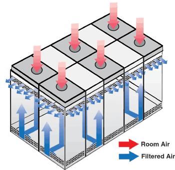
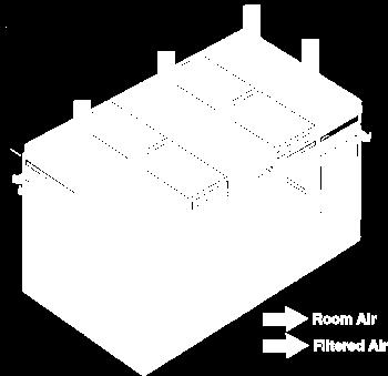
5 Clean room & HEPA filter HEPA = high efficiency particulate air. 5
6 Lithography 1. photolithography 2. principle shadow, projection 3. tools 4. pattern transfer 5. resolution 6. next-gen 6
 yield-resolution trade-off CD λg g λ λ (µm) g (µm) CD (µm) 0.4 50 4.5 0.")
7 Shadow Contact: dust particles can be transferred between mask and wafer low yield Proximity: dust not transferred high yield (poor resolution due to diffraction) yield-resolution trade-off CD λg g λ λ (µm) g (µm) CD (µm)
")
 M:1 reduction")
8 Projection Stepper (step-and-repeat system) Image partitioning techniques for projection printing: (a) annual-field wafer scan, (b) 1:1 step-and-repeat, (c) M:1 reduction step-and-repeat, and (d) M:1 reduction step-and-scan. 8

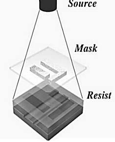
9 1. photolithography 2. principle 3. tools light source mask photoresist 4. pattern transfer 5. resolution 6. next-gen Lithography 9
10 Pre-1990: high-pressure mercury-arc lamp Mercury (Hg) source line λ(nm) G 436 H 405 I 365 source λ(nm) resolution (nm) Hg KrF ArF F Hg 10


11 Light source roadmap CMOS scaling necessitates the development of low-λ light source 11


12 1. photolithography 2. principle 3. tools light source mask photoresist 4. pattern transfer 5. resolution 6. next-gen Lithography ITRS2009. Table LITH5A 12


13 Mask How to make masks? Mask blank electron-beam lithography IC Mask (reticle) [Cr / SiO 2 ] [CAD] info, alignment marks, test structures, etc. alignment marks test structures 13
14 Yield see fig. [B] slide #3 Yield for a 10-mask lithographic process with various defect densities per level. the yield of a lithographic step depends critically on mask cleanliness, or how many fatal defects are presence: In order to improve yield, masks are cleaned / inspected regularly 14

15 1. photolithography 2. principle 3. tools light source mask photoresist 4. pattern transfer 5. resolution 6. next-gen Lithography source: ITRS2011, Table LITH3A 15
 or opposite to ( ) those on mask.")

16 Photoresist There are two types of resists: positive and negative. The final pattern on wafer is the same as (+) or opposite to ( ) those on mask. It is called photo-resist because: photo it responds to photons resist it resists etching / dopant atoms, protecting the layer underneath Suppliers: AZ, Shipley, Sumitomo photo resist 16
 Positive photoresist; (b) negative photoresist.")
17 The quality of the resist and the exposure / development process is measured by the steepness of the resist wall, or the contrast ratio: Figure Exposure-response curve and cross section of the resist image after development. 1 (a) Positive photoresist; (b) negative photoresist. source: ITRS2011, Table LITH3B 17
18 1. photolithography 2. principle 3. tools 4. pattern transfer 5. resolution 6. next-gen Lithography 18
![Pattern transfer transfers the pattern which appears on the photoresist onto the substrate (Si). The transfer process can be subtractive [A], or additive [B] in nature.](/docs-images/76/74336434/images/19-1.jpg "[A] Subtractive: etching (for oxide removal, interconnect) [B] Additive: metallization (S/D metal, via filling) Lift-Off process Some process (such as doping through photoresist) is neither")
19 Pattern transfer transfers the pattern which appears on the photoresist onto the substrate (Si). The transfer process can be subtractive [A], or additive [B] in nature. [A] Subtractive: etching (for oxide removal, interconnect) [B] Additive: metallization (S/D metal, via filling) Lift-Off process Some process (such as doping through photoresist) is neither subtractive nor additive. 19

20 source: ITRS2011, Fig. LITH1 20
21 Lithography 1. photolithography 2. principle 3. tools 4. pattern transfer 5. resolution limit enhancement (PSM, OPC, Immersion) 6. next-gen 21
22 Resolution of photolithography minimum printed line / feature size / resolution (l m ) trigonometry: λ l m = k1 NA NA = nsinθ DOF = k 2 λ ( NA) 2 NA: numerical aperture DOF: depth of focus Q) How to improve resolution (l m )? A) λ, NA Requirements: l m,, DOF 22

23 Diffraction diffraction is the limiting factor in printing two closely-spaced lines. Diffraction strong when L ~< λ mask wafer λ L L > λ L λ 23
24 Lithography 1. photolithography 2. principle 3. tools 4. pattern transfer 5. resolution limit enhancement (PSM, OPC, Immersion) 6. next-gen 24


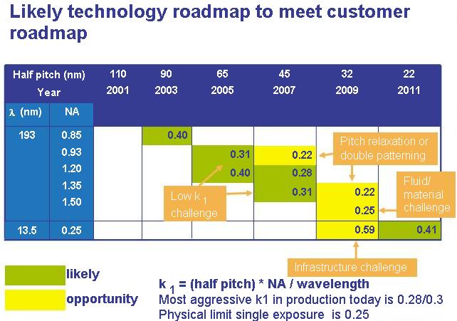
25 source: ITRS2009, Table LITH1 25

26 Resolution Enhancement Techniques A schematic of an optical lithography system showing the methods that can improve the technique's performance. Key: λ is the wavelength of the illumination source; OAIis offaxis illumination; IIL is imaging interferometric illumination; OPC is optical proximity correction; and PSM is phase-shift masks. Link 26
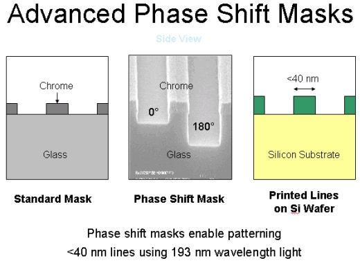
27 Phase-Shift Mask (PSM) diffraction intensity d = λ/2(n-1) Figure The principle of phase-shift technology. (a) Conventional technology; (b) phase-shift technology. 9 27
28 28


29 Optical Proximity Correction (OPC) a purely mathematical process The automated algorithmic link between DesignGauge, the application system for CD scanning electron microscopy (CD-SEM), and Proteus OPC for pre-processing OPC model building data allows Proteus customers to seamlessly obtain a large sampling of metrology data to account for process variations across the entire process window. 29


30 Immersion λ l m = k1 NA NA = nsinθ use n > 1 30


31 source: ITRS2011, Table LITH2 31

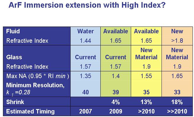
32 High-Index Lenses Push Immersion Beyond 32 nm Aaron Hand -- Semiconductor International, 4/1/2006 water's refractive index (n) = 1.44 high-index fluids n~1.65 photoresist n = 1.7 lens (n=1.56) becomes the limiter: calcium fluoride (CaF2) higher-index lens materials: lutetium aluminum garnet (LuAG), n =
33 33
34 Lithography 1. photolithography 2. principle 3. tools 4. pattern transfer 5. resolution 6. next-gen EUV, XRL, EBL, IBL, NIL 34


35 source: ITRS2011, Fig. LITH3A source: ITRS2011, Fig. LITH3B 35


36 EUV: extreme-ultra violet lithography In an laser produced plasma (LPP)-based system, EUV light is produced by bombarding a sliver of tin with a high-power laser. The light is then gathered by specially engineered EUV mirrors, which then focus an EUV beam in the EUV scanner to produce microchip patterns. ITRS2009: Table LITH5C 36

37 XRL: X-ray lithography 37
38 EBL: electron-beam lithography Schematic of an electron-beam machine. Direct-write (serial) Figure Schematic of positive and negative resists used in electron-beam lithography. 38
39 EBL: parallel Basic SCALPEL principle of operation showing contrast generation by differentiating more- or less-scattered electrons. Scattering with angular limitation projection electron beam lithography system R SiN x nm small scattering angle L Cr/W 30-60nm large scattering angle L 100 kev R 39
40 IBL: ion-beam lithography IBL: Trajectories of 60 kev H* ions traveling through PMMA into Au, Si, and PMMA. 18 EBL: Proximity effect: (a) Simulated trajectories of 100 electrons in PMMA for a 20-keV electron beam. 15 (b) Dose distribution for forward scattering and backscattering at the resist-substrate interface. 40
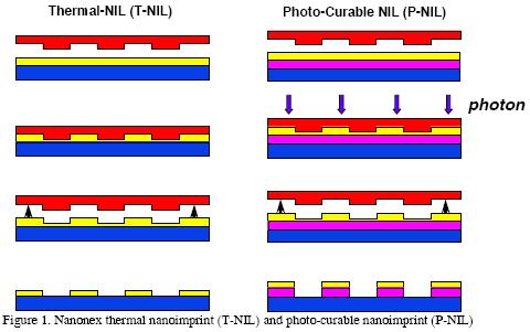

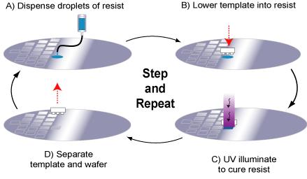
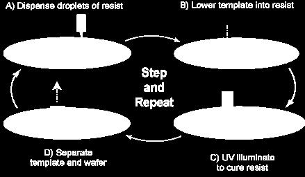
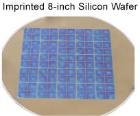
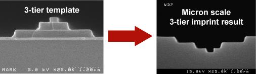
41 NIL: Nano-imprint lithography ITRS2009: Table LITH5D 41


42 42
43 photolithography process, principle, tools resolution limits Conclusions resolution-enhancement techniques PSM, OPC, Immersion, DP, future lithographic systems EUV, XRL, ML2 (EBL, IBL), NIL,... from ITRS2009:... To continue as the dominant technique for leading-edge critical layer lithography, resolution enhancement techniques (RETs) such as off-axis illumination (OAI), phase shifting masks (PSMs), and optical proximity corrections (OPCs) are being used with imaging systems at the 193 nm wavelength. In addition to RETs, lenses with increasing numerical apertures and decreasing aberrations will be required to extend the life of optical lithography. Liquid immersion imaging with a fluid between the final lens element and the wafer is also being used to extend optical lithography. 43
Section 2: Lithography. Jaeger Chapter 2 Litho Reader. The lithographic process
 Section 2: Lithography Jaeger Chapter 2 Litho Reader The lithographic process Photolithographic Process (a) (b) (c) (d) (e) (f) (g) Substrate covered with silicon dioxide barrier layer Positive photoresist
Optical Lithography. Keeho Kim Nano Team / R&D DongbuAnam Semi
 Optical Lithography Keeho Kim Nano Team / R&D DongbuAnam Semi Contents Lithography = Photolithography = Optical Lithography CD : Critical Dimension Resist Pattern after Development Exposure Contents Optical
MICROCHIP MANUFACTURING by S. Wolf
 MICROCHIP MANUFACTURING by S. Wolf Chapter 19 LITHOGRAPHY II: IMAGE-FORMATION and OPTICAL HARDWARE 2004 by LATTICE PRESS CHAPTER 19 - CONTENTS Preliminaries: Wave- Motion & The Behavior of Light Resolution
EE143 Fall 2016 Microfabrication Technologies. Lecture 3: Lithography Reading: Jaeger, Chap. 2
 EE143 Fall 2016 Microfabrication Technologies Lecture 3: Lithography Reading: Jaeger, Chap. 2 Prof. Ming C. Wu wu@eecs.berkeley.edu 511 Sutardja Dai Hall (SDH) 1-1 The lithographic process 1-2 1 Photolithographic
Section 2: Lithography. Jaeger Chapter 2 Litho Reader. EE143 Ali Javey Slide 5-1
 Section 2: Lithography Jaeger Chapter 2 Litho Reader EE143 Ali Javey Slide 5-1 The lithographic process EE143 Ali Javey Slide 5-2 Photolithographic Process (a) (b) (c) (d) (e) (f) (g) Substrate covered
Section 2: Lithography. Jaeger Chapter 2. EE143 Ali Javey Slide 5-1
 Section 2: Lithography Jaeger Chapter 2 EE143 Ali Javey Slide 5-1 The lithographic process EE143 Ali Javey Slide 5-2 Photolithographic Process (a) (b) (c) (d) (e) (f) (g) Substrate covered with silicon
Lithography. 3 rd. lecture: introduction. Prof. Yosi Shacham-Diamand. Fall 2004
 Lithography 3 rd lecture: introduction Prof. Yosi Shacham-Diamand Fall 2004 1 List of content Fundamental principles Characteristics parameters Exposure systems 2 Fundamental principles Aerial Image Exposure
Update on 193nm immersion exposure tool
 Update on 193nm immersion exposure tool S. Owa, H. Nagasaka, Y. Ishii Nikon Corporation O. Hirakawa and T. Yamamoto Tokyo Electron Kyushu Ltd. January 28, 2004 Litho Forum 1 What is immersion lithography?
ECSE 6300 IC Fabrication Laboratory Lecture 3 Photolithography. Lecture Outline
 ECSE 6300 IC Fabrication Laboratory Lecture 3 Photolithography Prof. James J. Q. Lu Bldg. CII, Rooms 6229 Rensselaer Polytechnic Institute Troy, NY 12180 Tel. (518)276 2909 e mails: luj@rpi.edu http://www.ecse.rpi.edu/courses/s18/ecse
NANOFABRICATION, THE NEW GENERATION OF LITHOGRAPHY. Cheng-Sheng Huang & Alvin Chang ABSTRACT
 NANOFABRICATION, THE NEW GENERATION OF LITHOGRAPHY Cheng-Sheng Huang & Alvin Chang ABSTRACT Fabrication on the micro- and nano-structure has opened the new horizons in science and engineering. The success
Photolithography II ( Part 2 )
") 1 Photolithography II ( Part 2 ) Chapter 14 : Semiconductor Manufacturing Technology by M. Quirk & J. Serda Saroj Kumar Patra, Department of Electronics and Telecommunication, Norwegian University of Science
1 Photolithography II ( Part 2 ) Chapter 14 : Semiconductor Manufacturing Technology by M. Quirk & J. Serda Saroj Kumar Patra, Department of Electronics and Telecommunication, Norwegian University of Science
Major Fabrication Steps in MOS Process Flow
 Major Fabrication Steps in MOS Process Flow UV light Mask oxygen Silicon dioxide photoresist exposed photoresist oxide Silicon substrate Oxidation (Field oxide) Photoresist Coating Mask-Wafer Alignment
Lecture 8. Microlithography
 Lecture 8 Microlithography Lithography Introduction Process Flow Wafer Exposure Systems Masks Resists State of the Art Lithography Next Generation Lithography (NGL) Recommended videos: http://www.youtube.com/user/asmlcompany#p/search/1/jh6urfqt_d4
Part 5-1: Lithography
 Part 5-1: Lithography Yao-Joe Yang 1 Pattern Transfer (Patterning) Types of lithography systems: Optical X-ray electron beam writer (non-traditional, no masks) Two-dimensional pattern transfer: limited
State-of-the-art device fabrication techniques
 State-of-the-art device fabrication techniques! Standard Photo-lithography and e-beam lithography! Advanced lithography techniques used in semiconductor industry Deposition: Thermal evaporation, e-gun
Optical Microlithography XXVIII
 PROCEEDINGS OF SPIE Optical Microlithography XXVIII Kafai Lai Andreas Erdmann Editors 24-26 February 2015 San Jose, California, United States Sponsored by SPIE Cosponsored by Cymer, an ASML company (United
Optical Lithography. Here Is Why. Burn J. Lin SPIE PRESS. Bellingham, Washington USA
 Optical Lithography Here Is Why Burn J. Lin SPIE PRESS Bellingham, Washington USA Contents Preface xiii Chapter 1 Introducing Optical Lithography /1 1.1 The Role of Lithography in Integrated Circuit Fabrication
Lecture 7. Lithography and Pattern Transfer. Reading: Chapter 7
 Lecture 7 Lithography and Pattern Transfer Reading: Chapter 7 Used for Pattern transfer into oxides, metals, semiconductors. 3 types of Photoresists (PR): Lithography and Photoresists 1.) Positive: PR
Photolithography I ( Part 1 )
") 1 Photolithography I ( Part 1 ) Chapter 13 : Semiconductor Manufacturing Technology by M. Quirk & J. Serda Bjørn-Ove Fimland, Department of Electronics and Telecommunication, Norwegian University of Science
1 Photolithography I ( Part 1 ) Chapter 13 : Semiconductor Manufacturing Technology by M. Quirk & J. Serda Bjørn-Ove Fimland, Department of Electronics and Telecommunication, Norwegian University of Science
Photolithography 光刻 Part I: Optics
 微纳光电子材料与器件工艺原理 Photolithography 光刻 Part I: Optics Xing Sheng 盛兴 Department of Electronic Engineering Tsinghua University xingsheng@tsinghua.edu.cn 1 Integrate Circuits Moore's law transistor number transistor
Process Optimization
 Process Optimization Process Flow for non-critical layer optimization START Find the swing curve for the desired resist thickness. Determine the resist thickness (spin speed) from the swing curve and find
Micro- and Nano-Technology... for Optics
 Micro- and Nano-Technology...... for Optics 3.2 Lithography U.D. Zeitner Fraunhofer Institut für Angewandte Optik und Feinmechanik Jena Printing on Stones Map of Munich Stone Print Contact Printing light
What s So Hard About Lithography?
 What s So Hard About Lithography? Chris A. Mack, www.lithoguru.com, Austin, Texas Optical lithography has been the mainstay of semiconductor patterning since the early days of integrated circuit production.
immersion optics Immersion Lithography with ASML HydroLith TWINSCAN System Modifications for Immersion Lithography by Bob Streefkerk
 immersion optics Immersion Lithography with ASML HydroLith by Bob Streefkerk For more than 25 years, many in the semiconductor industry have predicted the end of optical lithography. Recent developments,
Module 11: Photolithography. Lecture 14: Photolithography 4 (Continued)
") Module 11: Photolithography Lecture 14: Photolithography 4 (Continued) 1 In the previous lecture, we have discussed the utility of the three printing modes, and their relative advantages and disadvantages.
Module 11: Photolithography Lecture 14: Photolithography 4 (Continued) 1 In the previous lecture, we have discussed the utility of the three printing modes, and their relative advantages and disadvantages.
Photolithography. References: Introduction to Microlithography Thompson, Willson & Bowder, 1994
 Photolithography References: Introduction to Microlithography Thompson, Willson & Bowder, 1994 Microlithography, Science and Technology Sheats & Smith, 1998 Any other Microlithography or Photolithography
Institute of Solid State Physics. Technische Universität Graz. Lithography. Peter Hadley
 Technische Universität Graz Institute of Solid State Physics Lithography Peter Hadley http://www.cleanroom.byu.edu/virtual_cleanroom.parts/lithography.html http://www.cleanroom.byu.edu/su8.phtml Spin coater
Semiconductor Manufacturing Technology. Semiconductor Manufacturing Technology. Photolithography: Resist Development and Advanced Lithography
 Semiconductor Manufacturing Technology Michael Quirk & Julian Serda October 2001 by Prentice Hall Chapter 15 Photolithography: Resist Development and Advanced Lithography Eight Basic Steps of Photolithography
INTERNATIONAL TECHNOLOGY ROADMAP LITHOGRAPHY FOR SEMICONDUCTORS 2009 EDITION
 INTERNATIONAL TECHNOLOGY ROADMAP FOR SEMICONDUCTORS 2009 EDITION LITHOGRAPHY THE ITRS IS DEVISED AND INTENDED FOR TECHNOLOGY ASSESSMENT ONLY AND IS WITHOUT REGARD TO ANY COMMERCIAL CONSIDERATIONS PERTAINING
Micro- and Nano-Technology... for Optics
 Micro- and Nano-Technology...... for Optics 3.2 Lithography U.D. Zeitner Fraunhofer Institut für Angewandte Optik und Feinmechanik Jena Printing on Stones Map of Munich Stone Print Shadow Printing Photomask
Nanotechnology I+II 2006 / 07
 Nanotechnology for engineers Winter semester 2006-2007 Nanotechnology I+II 2006 / 07 Juergen Brugger & Patrik Hoffmann & Teams Course agenda (winter semester) Nanotechnology I winter semester (23.10.06-9.2.06)
Device Fabrication: Photolithography
 Device Fabrication: Photolithography 1 Objectives List the four components of the photoresist Describe the difference between +PR and PR Describe a photolithography process sequence List four alignment
Lecture 5. Optical Lithography
 Lecture 5 Optical Lithography Intro For most of microfabrication purposes the process (e.g. additive, subtractive or implantation) has to be applied selectively to particular areas of the wafer: patterning
Discovering Electrical & Computer Engineering. Carmen S. Menoni Professor Week 3 armain.
 Discovering Electrical & Computer Engineering Carmen S. Menoni Professor Week 3 http://www.engr.colostate.edu/ece103/semin armain.html TOP TECH 2012 SPECIAL REPORT IEEE SPECTRUM PAGE 28, JANUARY 2012 P.E.
Mask Technology Development in Extreme-Ultraviolet Lithography
 Mask Technology Development in Extreme-Ultraviolet Lithography Anthony Yen September 6, 2013 Projected End of Optical Lithography 2013 TSMC, Ltd 1976 1979 1982 1985 1988 1991 1994 1997 2000 2003 2007 2012
Photolithography Technology and Application
 Photolithography Technology and Application Jeff Tsai Director, Graduate Institute of Electro-Optical Engineering Tatung University Art or Science? Lind width = 100 to 5 micron meter!! Resolution = ~ 3
Lithography Is the Designer s Brush. Lithography is indispensible for defining locations and configurations of circuit elements/functions.
 Lithography 1 Lithography Is the Designer s Brush Lithography is indispensible for defining locations and configurations of circuit elements/functions. 2 ITRS 2007 The major challenge in litho: CD, CD
Lecture 13 Basic Photolithography
 Lecture 13 Basic Photolithography Chapter 12 Wolf and Tauber 1/64 Announcements Homework: Homework 3 is due today, please hand them in at the front. Will be returned one week from Thursday (16 th Nov).
Chapter 6. Photolithography
 Chapter 6 Photolithography 2006/4/10 1 Objectives List the four components of the photoresist Describe the difference between +PR and PR Describe a photolithography process sequence List four alignment
Optolith 2D Lithography Simulator
 2D Lithography Simulator Advanced 2D Optical Lithography Simulator 4/13/05 Introduction is a powerful non-planar 2D lithography simulator that models all aspects of modern deep sub-micron lithography It
Optical Issues in Photolithography
 OpenStax-CNX module: m25448 1 Optical Issues in Photolithography Andrew R. Barron This work is produced by OpenStax-CNX and licensed under the Creative Commons Attribution License 3.0 note: This module
EE-527: MicroFabrication
 EE-57: MicroFabrication Exposure and Imaging Photons white light Hg arc lamp filtered Hg arc lamp excimer laser x-rays from synchrotron Electrons Ions Exposure Sources focused electron beam direct write
Copyright 2004 by the Society of Photo-Optical Instrumentation Engineers.
 Copyright 2004 by the Society of Photo-Optical Instrumentation Engineers. This paper was published in the proceedings of Emerging Lithographic Technologies VIII, SPIE Vol. 5374, pp. 1-8. It is made available
FABRICATION OF CMOS INTEGRATED CIRCUITS. Dr. Mohammed M. Farag
 FABRICATION OF CMOS INTEGRATED CIRCUITS Dr. Mohammed M. Farag Outline Overview of CMOS Fabrication Processes The CMOS Fabrication Process Flow Design Rules Reference: Uyemura, John P. "Introduction to
EUVL Activities in China. Xiangzhao Wang Shanghai Inst. Of Opt. and Fine Mech. Of CAS. (SIOM) Shanghai, China.
 Shanghai, China.") EUVL Activities in China Xiangzhao Wang Shanghai Inst. Of Opt. and Fine Mech. Of CAS. (SIOM) Shanghai, China. wxz26267@siom.ac.cn Projection Optics Imaging System Surface Testing Optical Machining ML Coating
EUVL Activities in China Xiangzhao Wang Shanghai Inst. Of Opt. and Fine Mech. Of CAS. (SIOM) Shanghai, China. wxz26267@siom.ac.cn Projection Optics Imaging System Surface Testing Optical Machining ML Coating
Lithography. Development of High-Quality Attenuated Phase-Shift Masks
 Lithography S P E C I A L Development of High-Quality Attenuated Phase-Shift Masks by Toshihiro Ii and Masao Otaki, Toppan Printing Co., Ltd. Along with the year-by-year acceleration of semiconductor device
* AIT-5: Maskless, High-NA, Immersion, EUV, Imprint
 Advanced Issues and Technology (AIT) Modules Purpose: Explain the top advanced issues and concepts in optical projection printing and electron-beam lithography. AIT-1: LER and CAR AIT-2: Resolution Enhancement
Synthesis of projection lithography for low k1 via interferometry
 Synthesis of projection lithography for low k1 via interferometry Frank Cropanese *, Anatoly Bourov, Yongfa Fan, Andrew Estroff, Lena Zavyalova, Bruce W. Smith Center for Nanolithography Research, Rochester
Advanced Patterning Techniques for 22nm HP and beyond
 Advanced Patterning Techniques for 22nm HP and beyond An Overview IEEE LEOS (Bay Area) Yashesh A. Shroff Intel Corporation Aug 4 th, 2009 Outline The Challenge Advanced (optical) lithography overview Flavors
Outline. 1 Introduction. 2 Basic IC fabrication processes. 3 Fabrication techniques for MEMS. 4 Applications. 5 Mechanics issues on MEMS MDL NTHU
 Outline 1 Introduction 2 Basic IC fabrication processes 3 Fabrication techniques for MEMS 4 Applications 5 Mechanics issues on MEMS 2.2 Lithography Reading: Runyan Chap. 5, or 莊達人 Chap. 7, or Wolf and
2009 International Workshop on EUV Lithography
 Contents Introduction Absorber Stack Optimization Non-flatness Correction Blank Defect and Its Mitigation Wafer Printing Inspection Actinic Metrology Cleaning and Repair Status Remaining Issues in EUV
Module - 2 Lecture - 13 Lithography I
 Nano Structured Materials-Synthesis, Properties, Self Assembly and Applications Prof. Ashok. K.Ganguli Department of Chemistry Indian Institute of Technology, Delhi Module - 2 Lecture - 13 Lithography
Nano Fabrication. ChiiDong Chen Institute of Physics, Academia Sinica
 Nano Fabrication ChiiDong Chen Institute of Physics, Academia Sinica e-mail: chiidong@phys.sinica.edu.tw Web: http://www.phys.sinica.edu.tw/~quela TEL : 02 2789 6766 State-of-the-art device fabrication
Semiconductor Technology
 Semiconductor Technology from A to Z + - x 1 0 x Photolithographie www.halbleiter.org Contents Contents List of Figures III 1 Photolithographie 1 1.1 Exposure and resist coating..........................
EUVL getting ready for volume introduction
 EUVL getting ready for volume introduction SEMICON West 2010 Hans Meiling, July 14, 2010 Slide 1 public Outline ASML s Lithography roadmap to support Moore s Law Progress on 0.25NA EUV systems Progress
Project Staff: Timothy A. Savas, Michael E. Walsh, Thomas B. O'Reilly, Dr. Mark L. Schattenburg, and Professor Henry I. Smith
 9. Interference Lithography Sponsors: National Science Foundation, DMR-0210321; Dupont Agreement 12/10/99 Project Staff: Timothy A. Savas, Michael E. Walsh, Thomas B. O'Reilly, Dr. Mark L. Schattenburg,
Optical Requirements
 Optical Requirements Transmission vs. Film Thickness A pellicle needs a good light transmission and long term transmission stability. Transmission depends on the film thickness, film material and any anti-reflective
MICRO AND NANOPROCESSING TECHNOLOGIES
 MICRO AND NANOPROCESSING TECHNOLOGIES LECTURE 4 Optical lithography Concepts and processes Lithography systems Fundamental limitations and other issues Photoresists Photolithography process Process parameter
Amphibian XIS: An Immersion Lithography Microstepper Platform
 Amphibian XIS: An Immersion Lithography Microstepper Platform Bruce W. Smith, Anatoly Bourov, Yongfa Fan, Frank Cropanese, Peter Hammond Rochester Institute of Technology, Microelectronic Engineering Department,
Imec pushes the limits of EUV lithography single exposure for future logic and memory
 Edition March 2018 Semiconductor technology & processing Imec pushes the limits of EUV lithography single exposure for future logic and memory Imec has made considerable progress towards enabling extreme
Chapter 2 Silicon Planar Processing and Photolithography
 Chapter 2 Silicon Planar Processing and Photolithography The success of the electronics industry has been due in large part to advances in silicon integrated circuit (IC) technology based on planar processing,
Newer process technology (since 1999) includes :
 includes :") Newer process technology (since 1999) includes : copper metalization hi-k dielectrics for gate insulators si on insulator strained silicon lo-k dielectrics for interconnects Immersion lithography for masks
Newer process technology (since 1999) includes : copper metalization hi-k dielectrics for gate insulators si on insulator strained silicon lo-k dielectrics for interconnects Immersion lithography for masks
Tutor43.doc; Version 8/15/03 T h e L i t h o g r a p h y E x p e r t (November 2003)
") Tutor43.doc; Version /15/03 T h e L i t h o g r a p h y E x p e r t (November 2003) Scattering Bars Chris A. Mack, KLA-Tencor, FINLE Division, Austin, Texas Resolution enhancement technologies refer to
Tutor43.doc; Version /15/03 T h e L i t h o g r a p h y E x p e r t (November 2003) Scattering Bars Chris A. Mack, KLA-Tencor, FINLE Division, Austin, Texas Resolution enhancement technologies refer to
THE CHARACTERIZATION OF CHROMELESS PHASE SHIFT MASK TECHNIQUE FOR SUB-45NM LITHOGRAPHY TAN SOON YOENG
 THE CHARACTERIZATION OF CHROMELESS PHASE SHIFT MASK TECHNIQUE FOR SUB-45NM LITHOGRAPHY TAN SOON YOENG NATIONAL UNIVERSITY OF SINGAPORE 2008 THE CHARACTERIZATION OF CHROMELESS PHASE SHIFT MASK TECHNIQUE
TECHNOLOGY ROADMAP 2006 UPDATE LITHOGRAPHY FOR
 INTERNATIONAL TECHNOLOGY ROADMAP FOR SEMICONDUCTORS 2006 UPDATE LITHOGRAPHY THE ITRS IS DEVISED AND INTENDED FOR TECHNOLOGY ASSESSMENT ONLY AND IS WITHOUT REGARD TO ANY COMMERCIAL CONSIDERATIONS PERTAINING
Chapter 6 Photolithography
 Chapter 6 Photolithography Hong Xiao, Ph. D. hxiao89@hotmail.com www2.austin.cc.tx.us/hongxiao/book.htm Hong Xiao, Ph. D. www2.austin.cc.tx.us/hongxiao/book.htm 1 Objectives List the four components of
Electron Multi-Beam Technology for Mask and Wafer Direct Write. Elmar Platzgummer IMS Nanofabrication AG
 Electron Multi-Beam Technology for Mask and Wafer Direct Write Elmar Platzgummer IMS Nanofabrication AG Contents 2 Motivation for Multi-Beam Mask Writer (MBMW) MBMW Tool Principles and Architecture MBMW
Micro- and Nano- Fabrication and Replication Techniques
 Micro- and Nano- Fabrication and Replication Techniques Why do we have to write thing small and replicate fast? Plenty of Room at the Bottom Richard P. Feynman, December 1959 How do we write it? We have
Recent Development Activities on EUVL at ASET
 Title Recent Development Activities on at ASET Shinji Okazaki ASET Laboratory 2 nd International Workshop on 1 Overall Development Plan 98 99 00 01 02 03 04 05 06 07 08 ASET Basic Technologies 100% Government
From ArF Immersion to EUV Lithography
 From ArF Immersion to EUV Lithography Luc Van den hove Vice President IMEC Outline Introduction 193nm immersion lithography EUV lithography Global collaboration Conclusions Lithography is enabling 1000
Clean Room Technology Optical Lithography. Lithography I. takenfrombdhuey
 Clean Room Technology Optical Lithography Lithography I If the automobile had followed the same development cycle as the computer, a Rolls Royce would today cost $100, get a million miles per gallon, and
PHGN/CHEN/MLGN 435/535: Interdisciplinary Silicon Processing Laboratory. Simple Si solar Cell!
 Where were we? Simple Si solar Cell! Two Levels of Masks - photoresist, alignment Etch and oxidation to isolate thermal oxide, deposited oxide, wet etching, dry etching, isolation schemes Doping - diffusion/ion
Holistic View of Lithography for Double Patterning. Skip Miller ASML
 Holistic View of Lithography for Double Patterning Skip Miller ASML Outline Lithography Requirements ASML Holistic Lithography Solutions Conclusions Slide 2 Shrink Continues Lithography keeps adding value
TECHNOLOGY ROADMAP 2011 EDITION LITHOGRAPHY FOR
 INTERNATIONAL TECHNOLOGY ROADMAP FOR SEMICONDUCTORS 2011 EDITION LITHOGRAPHY THE ITRS IS DEVISED AND INTENDED FOR TECHNOLOGY ASSESSMENT ONLY AND IS WITHOUT REGARD TO ANY COMMERCIAL CONSIDERATIONS PERTAINING
Scope and Limit of Lithography to the End of Moore s Law
 Scope and Limit of Lithography to the End of Moore s Law Burn J. Lin tsmc, Inc. 1 What dictate the end of Moore s Law Economy Device limits Lithography limits 2 Litho Requirement of Critical Layers Logic
Reducing Proximity Effects in Optical Lithography
 INTERFACE '96 This paper was published in the proceedings of the Olin Microlithography Seminar, Interface '96, pp. 325-336. It is made available as an electronic reprint with permission of Olin Microelectronic
INTERNATIONAL TECHNOLOGY ROADMAP SEMICONDUCTORS 2001 EDITION LITHOGRAPHY FOR
 INTERNATIONAL TECHNOLOGY ROADMAP FOR SEMICONDUCTORS 2001 EDITION LITHOGRAPHY TABLE OF CONTENTS Scope...1 Difficult Challenges...1 Lithography Technology Requirements...3 Potential Solutions...14 Crosscut
Nanoscale Lithography. NA & Immersion. Trends in λ, NA, k 1. Pushing The Limits of Photolithography Introduction to Nanotechnology
 15-398 Introduction to Nanotechnology Nanoscale Lithography Seth Copen Goldstein Seth@cs.cmu.Edu CMU Pushing The Limits of Photolithography Reduce wavelength (λ) Use Reducing Lens Increase Numerical Aperture
Eun-Jin Kim, GukJin Kim, Seong-Sue Kim*, Han-Ku Cho*, Jinho Ahn**, Ilsin An, and Hye-Keun Oh
 Eun-Jin Kim, GukJin Kim, Seong-Sue Kim*, Han-Ku Cho*, Jinho Ahn**, Ilsin An, and Hye-Keun Oh Lithography Lab. Department of Applied Physics, Hanyang University, Korea *Samsung Electronics Co., LTD. Korea
Electron Beam Lithography. Adam Ramm
 Electron Beam Lithography Adam Ramm Why use electrons? Negligible diffraction limitations: R = k λ NA With current optical technology, this equates to about 45nm resolution. For an electron, wavelength
Advanced Device Fabrication Techniques. ChiiDong Chen
 Advanced Device Fabrication Techniques TIGP lecture, NTU 070501 ChiiDong Chen Institute of Physics, Academia Sinica e-mail: chiidong@phys.sinica.edu.tw url: www.phys.sinica.edu.tw/~quela Outline: 1 State-of-the-art
EUV Lithography Transition from Research to Commercialization
 EUV Lithography Transition from Research to Commercialization Charles W. Gwyn and Peter J. Silverman and Intel Corporation Photomask Japan 2003 Pacifico Yokohama, Kanagawa, Japan Gwyn:PMJ:4/17/03:1 EUV
attocfm I for Surface Quality Inspection NANOSCOPY APPLICATION NOTE M01 RELATED PRODUCTS G
 APPLICATION NOTE M01 attocfm I for Surface Quality Inspection Confocal microscopes work by scanning a tiny light spot on a sample and by measuring the scattered light in the illuminated volume. First,
T in sec, I in W/cm 2, E in J/cm 2
 Exposures from Mask Aligner into Resist Mask aligner images created by shadowing from mask into resist Soft contact and Proximity good for 3 micron structures Vacuum Hard Contact: no shadow effects at
ADVANCED TECHNOLOGY FOR EXTENDING OPTICAL LITHOGRAPHY
 ADVANCED TECHNOLOGY FOR EXTENDING OPTICAL LITHOGRAPHY Christian Wagner a, Winfried Kaiser a, Jan Mulkens b, Donis G. Flagello c a Carl Zeiss, D-73446 Oberkochen, Germany; b ASM Lithography, De Run 1110,
UV Nanoimprint Stepper Technology: Status and Roadmap. S.V. Sreenivasan Sematech Litho Forum May 14 th, 2008
 UV Nanoimprint Stepper Technology: Status and Roadmap S.V. Sreenivasan Sematech Litho Forum May 14 th, 2008 Overview Introduction Stepper technology status: Patterning and CD Control Through Etch Alignment
Advanced Digital Integrated Circuits. Lecture 2: Scaling Trends. Announcements. No office hour next Monday. Extra office hour Tuesday 2-3pm
 EE241 - Spring 20 Advanced Digital Integrated Circuits Lecture 2: Scaling Trends and Features of Modern Technologies Announcements No office hour next Monday Extra office hour Tuesday 2-3pm 2 1 Outline
EUVL Scanners Operational at Chipmakers. Skip Miller Semicon West 2011
 EUVL Scanners Operational at Chipmakers Skip Miller Semicon West 2011 Outline ASML s Lithography roadmap to support Moore s Law Progress on NXE:3100 (0.25NA) EUV systems Progress on NXE:3300 (0.33NA) EUV
Testing Aspheric Lenses: New Approaches
 Nasrin Ghanbari OPTI 521 - Synopsis of a published Paper November 5, 2012 Testing Aspheric Lenses: New Approaches by W. Osten, B. D orband, E. Garbusi, Ch. Pruss, and L. Seifert Published in 2010 Introduction
CHARACTERIZATION OF THE IMPACT OF SCATTERED LIGHT AND POWER ILLUMINATION NON UNIFORMITY ON SEMICONDUCTOR PROCESSES
 CHARACTERIZATION OF THE IMPACT OF SCATTERED LIGHT AND POWER ILLUMINATION NON UNIFORMITY ON SEMICONDUCTOR PROCESSES By Rajesh Joshi A thesis submitted in fulfillment of the requirement for the degree of
Nikon EUVL Development Progress Update
 Nikon EUVL Development Progress Update Takaharu Miura EUVL Symposium September 29, 2008 EUVL Symposium 2008 @Lake Tahoe T. Miura September 29, 2008 Slide 1 Presentation Outline 1. Nikon EUV roadmap 2.
Optical Waveguide Types
 8 Refractive Micro Optics Optical Waveguide Types There are two main types of optical waveguide structures: the step index and the graded index. In a step-index waveguide, the interface between the core
Lithographic Performance and Mix-and-Match Lithography using 100 kv Electron Beam System JBX-9300FS
 Lithographic Performance and Mix-and-Match Lithography using 100 kv Electron Beam System JBX-9300FS Yukinori Ochiai, Takashi Ogura, Mitsuru Narihiro, and Kohichi Arai Silicon Systems Research Laboratories,
Intel Technology Journal
 Volume 06 Issue 02 Published, May 16, 2002 ISSN 1535766X Intel Technology Journal Semiconductor Technology and Manufacturing The Intel Lithography Roadmap A compiled version of all papers from this issue
A review on contemporary practices in Lithography
 IOSR Journal of Applied Chemistry (IOSR-JAC) e-issn: 2278-5736.Volume 7, Issue 4 Ver. II. (Apr. 2014), PP 27-31 A review on contemporary practices in Lithography Perna Kishor Krishna, Mantha Anil Srimanth,
Sub-12nm Optical Lithography with 4x Pitch Division and SMO-Lite
 Sub-12nm Optical Lithography with 4x Pitch Division and SMO-Lite Michael C. Smayling* a, Koichiro Tsujita b, Hidetami Yaegashi c, Valery Axelrad d Tadashi Arai b, Kenichi Oyama c, Arisa Hara c a Tela Innovations,
Optical Projection Printing and Modeling
 Optical Projection Printing and Modeling Overview of optical lithography, concepts, trends Basic Parameters and Effects (1-14) Resolution Depth of Focus; Proximity, MEEF, LES Image Calculation, Characterization
Evaluation of Technology Options by Lithography Simulation
 Evaluation of Technology Options by Lithography Simulation Andreas Erdmann Fraunhofer IISB, Erlangen, Germany Semicon Europe, Dresden, October 12, 2011 Outline Introduction: Resolution limits of optical
Semiconductor Manufacturing and Inspection Technologies for the 0.1 µm Process Generation
 Hitachi Review Vol. 49 (2000), No. 4 199 Semiconductor Manufacturing and Inspection Technologies for the 0.1 µm Process Generation Takafumi Tokunaga Katsutaka Kimura Jun Nakazato Masaki Nagao, D. Eng.
TECHNOLOGY ROADMAP 2005 EDITION LITHOGRAPHY FOR
 INTERNATIONAL TECHNOLOGY ROADMAP FOR SEMICONDUCTORS 2005 EDITION LITHOGRAPHY THE ITRS IS DEVISED AND INTENDED FOR TECHNOLOGY ASSESSMENT ONLY AND IS WITHOUT REGARD TO ANY COMMERCIAL CONSIDERATIONS PERTAINING