Lecture 5. Optical Lithography
|
|
|
- Avis Kennedy
- 5 years ago
- Views:
Transcription
1 Lecture 5 Optical Lithography
2 Intro For most of microfabrication purposes the process (e.g. additive, subtractive or implantation) has to be applied selectively to particular areas of the wafer: patterning is required; Predominately done by optical lithography


3 Intro Patterns for lithography are usually designed where cells are assembled in the devices and repeated on the wafer Layout of cells is designed according to layout or design rules: smallest feature allowed smallest spacing allowed minimum overlap between the layers minimum spacing to underlying topology etc. Intel s Dual core CPU, 45nm tech, 420mln transistor each
 Optical tool: $20M")
4 Optical Lithography Roadmap g-line i-line DUV Today: Intel 45nm process, 157nm source wafer in use: 300mm diam processing steps per wafer: ~40 Costs: Mask cost: $ $ (!!!) Optical tool: $20M
5 Lecture plan Diffraction and the resolution limits Modulation transfer function Light sources Contact/proximity printers: Mask Aligners Projection printers: Steppers Advanced techniques: Phase-shift masks Immersion lithography Maskless lithography Stencil lithography ( Resistless )

6 Simple exposure system areal image of the mask


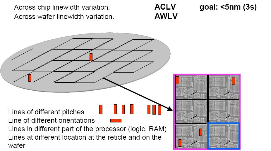
7 Performance issues Resolution: quoted as minimum feature size resolved maintaining a tolerance 6s<10% Registration: measure of overlay accuracy, usually 6s; Throughput: wafer/h for optical, <1 for ebeam Variation (within the chip, within the waferm wafer to wafer etc.)
8 Performance issues
9 as in 2003 reported by AMD Where we are now? wavelength NA Resolution Overlay CD-uniformity Development nm 20nm 6nm Production nm 30nm 8nm current projections
10 Requirements for the mask Required properties: high transparency at the exposure wavelength small thermal expansion coefficient flat highly polished surface Photomask material: fused silica glass (soda-lime) for NUV applications; opaque layer: usually chromium
 Waves from different sources will interfere with each other I = E + E + E E cos( φ φ ) 2 2 1 2 1 2 1")
11 Huygens Principle Resolution issues Generally, at a point r: Er (, ν ) = E( r)exp( jφ( r, ν)) 0 I r E r 2 () = ε 0 () Waves from different sources will interfere with each other I = E + E + E E cos( φ φ )
12 Resolution issues Near field (Mask close to wafer) Fresnel diffraction W λ g + r oscillations due to interference W+DW if W is very large and ray tracing can be used: g W = W D
 ( πyl λg) sin 2 sin 2 = ; Iy = 2πxW λg")
13 Far field (Fraunhofer diffraction) W λ g + r Resolution issues I x ( π xw λg) ( πyl λg) sin 2 sin 2 = ; Iy = 2πxW λg 2πyL λg
14 Resolution issues Other complications: light source is not a point imperfection of optical components reflection, adsorption, phase shift on the mask reflection on the wafer etc
15 Resolution issues Modulation transfer function (MTF) MTF I I max min = Imax + Imin measure of the optical contrast in the areal image The higher the MTF the better the contrast; The smaller the period of the grating, the lower is the MTF
, as the Intensity (or power density) times the exposure time.")
16 Resolution issues The MTF uses the power density (W/cm2 or (J/sec)/cm 2 ). The resist responds to the total amount of energy absorbed. Thus, we need to define the Dose, with units of energy density (mj/cm 2 ), as the Intensity (or power density) times the exposure time. We can also define D 100 = the minimum dose for which the photoresist will completely dissolve when developed. We define D 0 as the maximum energy density for which the photoresist will not dissolve at all when developed. Between these values, the photoresist will partially dissolve. Commonly, image with the MTF lower than 0.4 cannot be reproduced (of course depend on the resist system
 lithography equipment.")
 and electron transitions in Hg/Xe atoms Often particular lines are")
17 Light Source Typically mercury (Hg)- Xenon (Xe) vapor bulbs are used as a light source in visible (>420 nm) and ultraviolet (> nm and <420 nm) lithography equipment. Light is generated by: gray body radiation of electrons (40000K, lmax=75nm, absorbed by fused silica envelop, impurities added to reduce ozon production) and electron transitions in Hg/Xe atoms Often particular lines are filtered: 436 nm (g-line), 365 (i-line), 290, 280, 265 and 248 nm.
18 Light Source Schematics of contact/proximity printer

19 Light Sources Excimer lasers (excited dimers): brightest optical sources in UV based on excitation and breakage of dimeric molecules (like F 2, XeCl etc.) pumped by strobed kv arc lamps
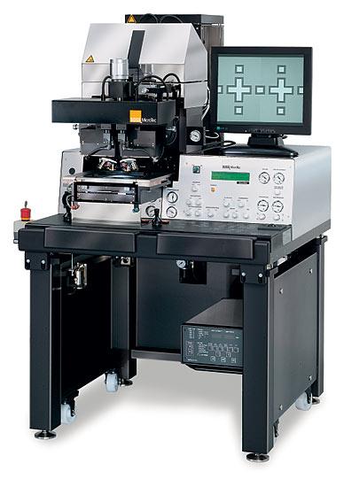
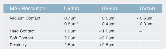
20 Contact/proximity printers Example: Carl Suss MA6 system

21 Contact/proximity printers W kλg constant ~1, depending on resist process Example: for k=1 and l=0.365 intensity vs. wafer position
22 Projection printers Rayleigh s criteria NA = nsin( α) Wmin λ k NA k is typically n DOF nλ 2 NA Köhler illumination
23 Projection printers Finite source effect: Dependence on the spatial coherence of the source For a source of finite size light will arrive with a different phase from different parts of the source! S = sourceimagediameter pupil diameter spatial frequency: ν ν ap 0 1 = 2W 1 = = W 0 NA 0.61λ

24 1:1 projection printers (1970) completely reflective optics (+) NA~0.16 very high throughput resolution ~2um global alignment Projection printers


25 Projection printers Canon 1x mirror projection system
 is exposed at a time high NA possible field leveling possible (so, high NA can be used)")
26 Projection printers: steppers small region of wafer (field cm2) is exposed at a time high NA possible field leveling possible (so, high NA can be used) Throughput 1 T = O+ n*[ E+ M + S+ A+ F]
27 Resolution improvement Wmin λ k NA reducing wavelength (193nm -> 157nm ->13.6 nm) increasing NA (but also decreasing the DOF) reducing k (depends on resist, mask, illumination, can be decreased from 1 down to 0.3.)

28 Advance mask concepts resolution improvement: phase shift mask Introduction of phase shifting regions on mask creates real zeros of the electrical field on the wafer => increased contrast
 Patterns")

29 Advance mask concepts Optical proximity correction (OPC) Patterns are distorted on mask in order to compensate limited resolution of optical system

30 Advance mask concepts Off-axis illumination Illumination under an angle brings enables transmission of first diffraction order through optical system


31 Surface reflection and standing waves reflection of surface topography features leads to poorly controlled linewidth standing waves can be formed

32 Surface reflection and standing waves Solution: antireflection coating on the wafer and/or on the resist (bottom/top ARC)
33 Immersion lithography

34 Immersion lithography improvement in resolution

35 concept Immersion lithography


36 Immersion lithography roadmap without immersion with immersion

37 Current Technology and Trends new systems under development
 H. Smith, MIT see R. Menon et al, Materials Today 4, p.26 (2005)")
38 Maskless lithography For low volume production maskless lithography can be advantageous (mainly due to high mask cost: per wafer cost ~$500 ($300 for the mask!) H. Smith, MIT see R. Menon et al, Materials Today 4, p.26 (2005)
, arrays are made on")
39 Fabrication of DNA arrays w. maskless lithography Fabrication of DNA array requires many lithographic steps (equal to number of bp), arrays are made on demand good candidate for maskless lithography S. Singh-Gasson et al, Nature Biotech., 17, p.974 (1999)
 might be damaged by standard")
 can be")
40 Stencil lithography biological or fragile object (e.g. membranes) might be damaged by standard resist processing techniques. Stencil lithography ( resistless ) can be advantageous for those objects.
41 Problems Campbell 7.4: In an effort to make a relatively inexpensive aligner, capable of producing very small features an optical source of a simple contact printer is replaced with ArF laser. list 2 problems that the engineer is likely to encounter in trying to use this device, assume yield is unimportant assume the resist constant 0.8 for the process and the gap equal to resist thickness in hard contact. What is the minimum feature size for 1um resist How thin the resist should be made to achieve 0.1um resolution Campbell 7.8 A particular resist process is able to resolve features whose MTF 0.3. Using fig 7.22 calculate the minimum feature size for an i-line aligner with NA=9.4 and S=0.5
Lecture 7. Lithography and Pattern Transfer. Reading: Chapter 7
 Lecture 7 Lithography and Pattern Transfer Reading: Chapter 7 Used for Pattern transfer into oxides, metals, semiconductors. 3 types of Photoresists (PR): Lithography and Photoresists 1.) Positive: PR
Lithography. 3 rd. lecture: introduction. Prof. Yosi Shacham-Diamand. Fall 2004
 Lithography 3 rd lecture: introduction Prof. Yosi Shacham-Diamand Fall 2004 1 List of content Fundamental principles Characteristics parameters Exposure systems 2 Fundamental principles Aerial Image Exposure
Section 2: Lithography. Jaeger Chapter 2 Litho Reader. The lithographic process
 Section 2: Lithography Jaeger Chapter 2 Litho Reader The lithographic process Photolithographic Process (a) (b) (c) (d) (e) (f) (g) Substrate covered with silicon dioxide barrier layer Positive photoresist
EE143 Fall 2016 Microfabrication Technologies. Lecture 3: Lithography Reading: Jaeger, Chap. 2
 EE143 Fall 2016 Microfabrication Technologies Lecture 3: Lithography Reading: Jaeger, Chap. 2 Prof. Ming C. Wu wu@eecs.berkeley.edu 511 Sutardja Dai Hall (SDH) 1-1 The lithographic process 1-2 1 Photolithographic
Section 2: Lithography. Jaeger Chapter 2 Litho Reader. EE143 Ali Javey Slide 5-1
 Section 2: Lithography Jaeger Chapter 2 Litho Reader EE143 Ali Javey Slide 5-1 The lithographic process EE143 Ali Javey Slide 5-2 Photolithographic Process (a) (b) (c) (d) (e) (f) (g) Substrate covered
MICRO AND NANOPROCESSING TECHNOLOGIES
 MICRO AND NANOPROCESSING TECHNOLOGIES LECTURE 4 Optical lithography Concepts and processes Lithography systems Fundamental limitations and other issues Photoresists Photolithography process Process parameter
Section 2: Lithography. Jaeger Chapter 2. EE143 Ali Javey Slide 5-1
 Section 2: Lithography Jaeger Chapter 2 EE143 Ali Javey Slide 5-1 The lithographic process EE143 Ali Javey Slide 5-2 Photolithographic Process (a) (b) (c) (d) (e) (f) (g) Substrate covered with silicon
Part 5-1: Lithography
 Part 5-1: Lithography Yao-Joe Yang 1 Pattern Transfer (Patterning) Types of lithography systems: Optical X-ray electron beam writer (non-traditional, no masks) Two-dimensional pattern transfer: limited
EE-527: MicroFabrication
 EE-57: MicroFabrication Exposure and Imaging Photons white light Hg arc lamp filtered Hg arc lamp excimer laser x-rays from synchrotron Electrons Ions Exposure Sources focused electron beam direct write
MICROCHIP MANUFACTURING by S. Wolf
 MICROCHIP MANUFACTURING by S. Wolf Chapter 19 LITHOGRAPHY II: IMAGE-FORMATION and OPTICAL HARDWARE 2004 by LATTICE PRESS CHAPTER 19 - CONTENTS Preliminaries: Wave- Motion & The Behavior of Light Resolution
Photolithography 光刻 Part I: Optics
 微纳光电子材料与器件工艺原理 Photolithography 光刻 Part I: Optics Xing Sheng 盛兴 Department of Electronic Engineering Tsinghua University xingsheng@tsinghua.edu.cn 1 Integrate Circuits Moore's law transistor number transistor
Photolithography I ( Part 1 )
") 1 Photolithography I ( Part 1 ) Chapter 13 : Semiconductor Manufacturing Technology by M. Quirk & J. Serda Bjørn-Ove Fimland, Department of Electronics and Telecommunication, Norwegian University of Science
1 Photolithography I ( Part 1 ) Chapter 13 : Semiconductor Manufacturing Technology by M. Quirk & J. Serda Bjørn-Ove Fimland, Department of Electronics and Telecommunication, Norwegian University of Science
Major Fabrication Steps in MOS Process Flow
 Major Fabrication Steps in MOS Process Flow UV light Mask oxygen Silicon dioxide photoresist exposed photoresist oxide Silicon substrate Oxidation (Field oxide) Photoresist Coating Mask-Wafer Alignment
ECSE 6300 IC Fabrication Laboratory Lecture 3 Photolithography. Lecture Outline
 ECSE 6300 IC Fabrication Laboratory Lecture 3 Photolithography Prof. James J. Q. Lu Bldg. CII, Rooms 6229 Rensselaer Polytechnic Institute Troy, NY 12180 Tel. (518)276 2909 e mails: luj@rpi.edu http://www.ecse.rpi.edu/courses/s18/ecse
Photolithography II ( Part 2 )
") 1 Photolithography II ( Part 2 ) Chapter 14 : Semiconductor Manufacturing Technology by M. Quirk & J. Serda Saroj Kumar Patra, Department of Electronics and Telecommunication, Norwegian University of Science
1 Photolithography II ( Part 2 ) Chapter 14 : Semiconductor Manufacturing Technology by M. Quirk & J. Serda Saroj Kumar Patra, Department of Electronics and Telecommunication, Norwegian University of Science
Lecture 13 Basic Photolithography
 Lecture 13 Basic Photolithography Chapter 12 Wolf and Tauber 1/64 Announcements Homework: Homework 3 is due today, please hand them in at the front. Will be returned one week from Thursday (16 th Nov).
Lecture 8. Microlithography
 Lecture 8 Microlithography Lithography Introduction Process Flow Wafer Exposure Systems Masks Resists State of the Art Lithography Next Generation Lithography (NGL) Recommended videos: http://www.youtube.com/user/asmlcompany#p/search/1/jh6urfqt_d4
Optical Lithography. Here Is Why. Burn J. Lin SPIE PRESS. Bellingham, Washington USA
 Optical Lithography Here Is Why Burn J. Lin SPIE PRESS Bellingham, Washington USA Contents Preface xiii Chapter 1 Introducing Optical Lithography /1 1.1 The Role of Lithography in Integrated Circuit Fabrication
Process Optimization
 Process Optimization Process Flow for non-critical layer optimization START Find the swing curve for the desired resist thickness. Determine the resist thickness (spin speed) from the swing curve and find
EE 143 Microfabrication Technology Fall 2014
 EE 143 Microfabrication Technology Fall 2014 Prof. Clark T.-C. Nguyen Dept. of Electrical Engineering & Computer Sciences University of California at Berkeley Berkeley, CA 94720 EE 143: Microfabrication
5. Lithography. 1. photolithography intro: overall, clean room 2. principle 3. tools 4. pattern transfer 5. resolution 6. next-gen
 5. Lithography 1. photolithography intro: overall, clean room 2. principle 3. tools 4. pattern transfer 5. resolution 6. next-gen References: Semiconductor Devices: Physics and Technology. 2 nd Ed. SM
Photolithography. References: Introduction to Microlithography Thompson, Willson & Bowder, 1994
 Photolithography References: Introduction to Microlithography Thompson, Willson & Bowder, 1994 Microlithography, Science and Technology Sheats & Smith, 1998 Any other Microlithography or Photolithography
Optical Projection Printing and Modeling
 Optical Projection Printing and Modeling Overview of optical lithography, concepts, trends Basic Parameters and Effects (1-14) Resolution Depth of Focus; Proximity, MEEF, LES Image Calculation, Characterization
Optical Lithography. Keeho Kim Nano Team / R&D DongbuAnam Semi
 Optical Lithography Keeho Kim Nano Team / R&D DongbuAnam Semi Contents Lithography = Photolithography = Optical Lithography CD : Critical Dimension Resist Pattern after Development Exposure Contents Optical
Microlithography. exposing radiation. mask. imaging system (low pass filter) photoresist. develop. etch
 photoresist. develop. etch") Microlithography Geometry Trends Master Patterns: Mask technology Pattern Transfer: Mask Aligner technology Wafer Transfer Media: Photo resist technology mask blank: transparent, mechanically rigid masking
Microlithography Geometry Trends Master Patterns: Mask technology Pattern Transfer: Mask Aligner technology Wafer Transfer Media: Photo resist technology mask blank: transparent, mechanically rigid masking
Purpose: Explain the top 10 phenomena and concepts. BPP-1: Resolution and Depth of Focus (1.5X)
") Basic Projection Printing (BPP) Modules Purpose: Explain the top 10 phenomena and concepts key to understanding optical projection printing BPP-1: Resolution and Depth of Focus (1.5X) BPP-2: Bragg condition
Basic Projection Printing (BPP) Modules Purpose: Explain the top 10 phenomena and concepts key to understanding optical projection printing BPP-1: Resolution and Depth of Focus (1.5X) BPP-2: Bragg condition
What s So Hard About Lithography?
 What s So Hard About Lithography? Chris A. Mack, www.lithoguru.com, Austin, Texas Optical lithography has been the mainstay of semiconductor patterning since the early days of integrated circuit production.
Innovative Mask Aligner Lithography for MEMS and Packaging
 Innovative Mask Aligner Lithography for MEMS and Packaging Dr. Reinhard Voelkel CEO SUSS MicroOptics SA September 9 th, 2010 1 SUSS Micro-Optics SUSS MicroOptics is a leading supplier for high-quality
Sub-50 nm period patterns with EUV interference lithography
 Microelectronic Engineering 67 68 (2003) 56 62 www.elsevier.com/ locate/ mee Sub-50 nm period patterns with EUV interference lithography * a, a a b b b H.H. Solak, C. David, J. Gobrecht, V. Golovkina,
Tutor43.doc; Version 8/15/03 T h e L i t h o g r a p h y E x p e r t (November 2003)
") Tutor43.doc; Version /15/03 T h e L i t h o g r a p h y E x p e r t (November 2003) Scattering Bars Chris A. Mack, KLA-Tencor, FINLE Division, Austin, Texas Resolution enhancement technologies refer to
Tutor43.doc; Version /15/03 T h e L i t h o g r a p h y E x p e r t (November 2003) Scattering Bars Chris A. Mack, KLA-Tencor, FINLE Division, Austin, Texas Resolution enhancement technologies refer to
Module 11: Photolithography. Lecture 14: Photolithography 4 (Continued)
") Module 11: Photolithography Lecture 14: Photolithography 4 (Continued) 1 In the previous lecture, we have discussed the utility of the three printing modes, and their relative advantages and disadvantages.
Module 11: Photolithography Lecture 14: Photolithography 4 (Continued) 1 In the previous lecture, we have discussed the utility of the three printing modes, and their relative advantages and disadvantages.
Micro- and Nano-Technology... for Optics
 Micro- and Nano-Technology...... for Optics 3.2 Lithography U.D. Zeitner Fraunhofer Institut für Angewandte Optik und Feinmechanik Jena Printing on Stones Map of Munich Stone Print Contact Printing light
Key Photolithographic Outputs
 Exposure latitude Depth of Focus Exposure latitude Vs DOF plot Linearity and MEEF Isolated-Dense Bias NILS Contrast Swing Curve Reflectivity Curve 1 Exposure latitude:the range of exposure energies (usually
Clean Room Technology Optical Lithography. Lithography I. takenfrombdhuey
 Clean Room Technology Optical Lithography Lithography I If the automobile had followed the same development cycle as the computer, a Rolls Royce would today cost $100, get a million miles per gallon, and
T in sec, I in W/cm 2, E in J/cm 2
 Exposures from Mask Aligner into Resist Mask aligner images created by shadowing from mask into resist Soft contact and Proximity good for 3 micron structures Vacuum Hard Contact: no shadow effects at
Optolith 2D Lithography Simulator
 2D Lithography Simulator Advanced 2D Optical Lithography Simulator 4/13/05 Introduction is a powerful non-planar 2D lithography simulator that models all aspects of modern deep sub-micron lithography It
Chapter 15 IC Photolithography
 Chapter 15 IC Photolithography Advances in integrated circuit density are driven by the self-fulfilling prophecy known as Moore s law, which specifies that there is an exponential increase in circuit density
T in sec, I in W/cm 2, E in J/cm 2
 Exposures from Mask Aligner into Resist Mask aligner images created by shadowing from mask into resist Soft contact and Proximity good for 3 micron structures Vacuum Hard Contact: no shadow effects at
Synthesis of projection lithography for low k1 via interferometry
 Synthesis of projection lithography for low k1 via interferometry Frank Cropanese *, Anatoly Bourov, Yongfa Fan, Andrew Estroff, Lena Zavyalova, Bruce W. Smith Center for Nanolithography Research, Rochester
Photolithography Technology and Application
 Photolithography Technology and Application Jeff Tsai Director, Graduate Institute of Electro-Optical Engineering Tatung University Art or Science? Lind width = 100 to 5 micron meter!! Resolution = ~ 3
Oriel Flood Exposure Sources
 218 Oriel Flood Exposure Sources High intensity outputs CALIBRATION SOURCES Highly uniform, large collimated beams Efficient out of band rejection Timed exposures DEUTERIUM SOURCES ARC SOURCES INCANDESCENT
Institute of Solid State Physics. Technische Universität Graz. Lithography. Peter Hadley
 Technische Universität Graz Institute of Solid State Physics Lithography Peter Hadley http://www.cleanroom.byu.edu/virtual_cleanroom.parts/lithography.html http://www.cleanroom.byu.edu/su8.phtml Spin coater
PHY 431 Homework Set #5 Due Nov. 20 at the start of class
 PHY 431 Homework Set #5 Due Nov. 0 at the start of class 1) Newton s rings (10%) The radius of curvature of the convex surface of a plano-convex lens is 30 cm. The lens is placed with its convex side down
Photolithography Module
 Electronics Workforce Development System Photolithography Module Introduction Photolithography Module This module will teach students the different types of microlithographic systems being used today,
Chapter 6. Photolithography
 Chapter 6 Photolithography 2006/4/10 1 Objectives List the four components of the photoresist Describe the difference between +PR and PR Describe a photolithography process sequence List four alignment
Refractive Power of a Surface. Exposure Sources. Thin Lenses. Thick Lenses. High Pressure Hg Arc Lamp Spectrum
 eractive Power o a Surace The reractive power P is measured in diopters when the radius is expressed in meters. n and n are the reractive indices o the two media. EE-57: icrofabrication n n P n n Exposure
TSMC Property. EUV Lithography. The March toward HVM. Anthony Yen. 9 September TSMC, Ltd
 EUV Lithography The March toward HVM Anthony Yen 9 September 2016 1 1 st EUV lithography setup and results, 1986 Si Stencil Mask SR W/C Multilayer Coating Optics λ=11 nm, provided by synchrotron radiation
Optical Issues in Photolithography
 OpenStax-CNX module: m25448 1 Optical Issues in Photolithography Andrew R. Barron This work is produced by OpenStax-CNX and licensed under the Creative Commons Attribution License 3.0 note: This module
NANOFABRICATION, THE NEW GENERATION OF LITHOGRAPHY. Cheng-Sheng Huang & Alvin Chang ABSTRACT
 NANOFABRICATION, THE NEW GENERATION OF LITHOGRAPHY Cheng-Sheng Huang & Alvin Chang ABSTRACT Fabrication on the micro- and nano-structure has opened the new horizons in science and engineering. The success
Optical Requirements
 Optical Requirements Transmission vs. Film Thickness A pellicle needs a good light transmission and long term transmission stability. Transmission depends on the film thickness, film material and any anti-reflective
Copyright 2000 by the Society of Photo-Optical Instrumentation Engineers.
 Copyright by the Society of Photo-Optical Instrumentation Engineers. This paper was published in the proceedings of Optical Microlithography XIII, SPIE Vol. 4, pp. 658-664. It is made available as an electronic
Module - 2 Lecture - 13 Lithography I
 Nano Structured Materials-Synthesis, Properties, Self Assembly and Applications Prof. Ashok. K.Ganguli Department of Chemistry Indian Institute of Technology, Delhi Module - 2 Lecture - 13 Lithography
Shot noise and process window study for printing small contacts using EUVL. Sang Hun Lee John Bjorkohlm Robert Bristol
 Shot noise and process window study for printing small contacts using EUVL Sang Hun Lee John Bjorkohlm Robert Bristol Abstract There are two issues in printing small contacts with EUV lithography (EUVL).
Design Rules for Silicon Photonics Prototyping
 Design Rules for licon Photonics Prototyping Version 1 (released February 2008) Introduction IME s Photonics Prototyping Service offers 248nm lithography based fabrication technology for passive licon-on-insulator
Device Fabrication: Photolithography
 Device Fabrication: Photolithography 1 Objectives List the four components of the photoresist Describe the difference between +PR and PR Describe a photolithography process sequence List four alignment
450mm and Moore s Law Advanced Packaging Challenges and the Impact of 3D
 450mm and Moore s Law Advanced Packaging Challenges and the Impact of 3D Doug Anberg VP, Technical Marketing Ultratech SOKUDO Lithography Breakfast Forum July 10, 2013 Agenda Next Generation Technology
Project Staff: Timothy A. Savas, Michael E. Walsh, Thomas B. O'Reilly, Dr. Mark L. Schattenburg, and Professor Henry I. Smith
 9. Interference Lithography Sponsors: National Science Foundation, DMR-0210321; Dupont Agreement 12/10/99 Project Staff: Timothy A. Savas, Michael E. Walsh, Thomas B. O'Reilly, Dr. Mark L. Schattenburg,
* AIT-5: Maskless, High-NA, Immersion, EUV, Imprint
 Advanced Issues and Technology (AIT) Modules Purpose: Explain the top advanced issues and concepts in optical projection printing and electron-beam lithography. AIT-1: LER and CAR AIT-2: Resolution Enhancement
Semiconductor Manufacturing Technology. Semiconductor Manufacturing Technology. Photolithography: Resist Development and Advanced Lithography
 Semiconductor Manufacturing Technology Michael Quirk & Julian Serda October 2001 by Prentice Hall Chapter 15 Photolithography: Resist Development and Advanced Lithography Eight Basic Steps of Photolithography
Near-field optical photomask repair with a femtosecond laser
 Journal of Microscopy, Vol. 194, Pt 2/3, May/June 1999, pp. 537 541. Received 6 December 1998; accepted 9 February 1999 Near-field optical photomask repair with a femtosecond laser K. LIEBERMAN, Y. SHANI,
More on the Mask Error Enhancement Factor
 T h e L i t h o g r a p h y E x p e r t (Fall 1999) More on the Mask Error Enhancement Factor Chris A. Mack, FINLE Technologies, Austin, Texas In a previous edition of this column (Winter, 1999) I described
200mm and 300mm Test Patterned Wafers for Bonding Process Applications SKW ASSOCIATES, INC.
 C M P C h a r a c t e r I z a t I o n S o l u t I o n s 200mm and 300mm Test Patterned Wafers for Bonding Process Applications SKW ASSOCIATES, INC. 2920 Scott Blvd., Santa Clara, CA 95054 Tel: 408-919-0094,
TECHNOLOGY ROADMAP 2006 UPDATE LITHOGRAPHY FOR
 INTERNATIONAL TECHNOLOGY ROADMAP FOR SEMICONDUCTORS 2006 UPDATE LITHOGRAPHY THE ITRS IS DEVISED AND INTENDED FOR TECHNOLOGY ASSESSMENT ONLY AND IS WITHOUT REGARD TO ANY COMMERCIAL CONSIDERATIONS PERTAINING
T in sec, I in W/cm 2, E in J/cm 2
 Exposures from Mask Aligner into Resist Mask aligner images created by shadowing from mask into resist Soft contact and Proximity good for 3 micron structures Vacuum Hard Contact: no shadow effects at
Applications of Maskless Lithography for the Production of Large Area Substrates Using the SF-100 ELITE. Jay Sasserath, PhD
 Applications of Maskless Lithography for the Production of Large Area Substrates Using the SF-100 ELITE Executive Summary Jay Sasserath, PhD Intelligent Micro Patterning LLC St. Petersburg, Florida Processing
Diffraction. Interference with more than 2 beams. Diffraction gratings. Diffraction by an aperture. Diffraction of a laser beam
 Diffraction Interference with more than 2 beams 3, 4, 5 beams Large number of beams Diffraction gratings Equation Uses Diffraction by an aperture Huygen s principle again, Fresnel zones, Arago s spot Qualitative
Will contain image distance after raytrace Will contain image height after raytrace
 Name: LASR 51 Final Exam May 29, 2002 Answer all questions. Module numbers are for guidance, some material is from class handouts. Exam ends at 8:20 pm. Ynu Raytracing The first questions refer to the
Micro- and Nano-Technology... for Optics
 Micro- and Nano-Technology...... for Optics 3.2 Lithography U.D. Zeitner Fraunhofer Institut für Angewandte Optik und Feinmechanik Jena Printing on Stones Map of Munich Stone Print Shadow Printing Photomask
Reducing Proximity Effects in Optical Lithography
 INTERFACE '96 This paper was published in the proceedings of the Olin Microlithography Seminar, Interface '96, pp. 325-336. It is made available as an electronic reprint with permission of Olin Microelectronic
Exercise 8: Interference and diffraction
 Physics 223 Name: Exercise 8: Interference and diffraction 1. In a two-slit Young s interference experiment, the aperture (the mask with the two slits) to screen distance is 2.0 m, and a red light of wavelength
Amphibian XIS: An Immersion Lithography Microstepper Platform
 Amphibian XIS: An Immersion Lithography Microstepper Platform Bruce W. Smith, Anatoly Bourov, Yongfa Fan, Frank Cropanese, Peter Hammond Rochester Institute of Technology, Microelectronic Engineering Department,
Experimental measurement of photoresist modulation curves
 Experimental measurement of photoresist modulation curves Anatoly Bourov *a,c, Stewart A. Robertson b, Bruce W. Smith c, Michael Slocum c, Emil C. Piscani c a Rochester Institute of Technology, 82 Lomb
PHGN/CHEN/MLGN 435/535: Interdisciplinary Silicon Processing Laboratory. Simple Si solar Cell!
 Where were we? Simple Si solar Cell! Two Levels of Masks - photoresist, alignment Etch and oxidation to isolate thermal oxide, deposited oxide, wet etching, dry etching, isolation schemes Doping - diffusion/ion
UV LED ILLUMINATION STEPPER OFFERS HIGH PERFORMANCE AND LOW COST OF OWNERSHIP
 UV LED ILLUMINATION STEPPER OFFERS HIGH PERFORMANCE AND LOW COST OF OWNERSHIP Casey Donaher, Rudolph Technologies Herbert J. Thompson, Rudolph Technologies Chin Tiong Sim, Rudolph Technologies Rudolph
MICROBUMP LITHOGRAPHY FOR 3D STACKING APPLICATIONS
 MICROBUMP LITHOGRAPHY FOR 3D STACKING APPLICATIONS Patrick Jaenen, John Slabbekoorn, Andy Miller IMEC Kapeldreef 75 B-3001 Leuven, Belgium millera@imec.be Warren W. Flack, Manish Ranjan, Gareth Kenyon,
Intel Technology Journal
 Volume 06 Issue 02 Published, May 16, 2002 ISSN 1535766X Intel Technology Journal Semiconductor Technology and Manufacturing The Intel Lithography Roadmap A compiled version of all papers from this issue
Copyright 2000, Society of Photo-Optical Instrumentation Engineers This paper was published in Optical Microlithography XIII, Volume 4000 and is made
 Copyright 00, Society of Photo-Optical Instrumentation Engineers This paper was published in Optical Microlithography XIII, Volume 4000 and is made available as an electronic reprint with permission of
Zone-plate-array lithography using synchrotron radiation
 Zone-plate-array lithography using synchrotron radiation A. Pépin, a) D. Decanini, and Y. Chen Laboratoire de Microstructures et de Microélectronique (L2M), CNRS, 196 avenue Henri-Ravéra, 92225 Bagneux,
Mask Technology Development in Extreme-Ultraviolet Lithography
 Mask Technology Development in Extreme-Ultraviolet Lithography Anthony Yen September 6, 2013 Projected End of Optical Lithography 2013 TSMC, Ltd 1976 1979 1982 1985 1988 1991 1994 1997 2000 2003 2007 2012
Dr. Dirk Meyners Prof. Wagner. Wagner / Meyners Micro / Nanosystems Technology
 Micro/Nanosystems Technology Dr. Dirk Meyners Prof. Wagner 1 Outline - Lithography Overview - UV-Lithography - Resolution Enhancement Techniques - Electron Beam Lithography - Patterning with Focused Ion
The End of Thresholds: Subwavelength Optical Linewidth Measurement Using the Flux-Area Technique
 The End of Thresholds: Subwavelength Optical Linewidth Measurement Using the Flux-Area Technique Peter Fiekowsky Automated Visual Inspection, Los Altos, California ABSTRACT The patented Flux-Area technique
Chapter 36: diffraction
 Chapter 36: diffraction Fresnel and Fraunhofer diffraction Diffraction from a single slit Intensity in the single slit pattern Multiple slits The Diffraction grating X-ray diffraction Circular apertures
THE CHARACTERIZATION OF CHROMELESS PHASE SHIFT MASK TECHNIQUE FOR SUB-45NM LITHOGRAPHY TAN SOON YOENG
 THE CHARACTERIZATION OF CHROMELESS PHASE SHIFT MASK TECHNIQUE FOR SUB-45NM LITHOGRAPHY TAN SOON YOENG NATIONAL UNIVERSITY OF SINGAPORE 2008 THE CHARACTERIZATION OF CHROMELESS PHASE SHIFT MASK TECHNIQUE
UV GAS LASERS PREPARED BY: STUDENT NO: COURSE NO: EEE 6503 COURSE TITLE: LASER THEORY
 UV GAS LASERS PREPARED BY: ISMAIL HOSSAIN FARHAD STUDENT NO: 0411062241 COURSE NO: EEE 6503 COURSE TITLE: LASER THEORY Introduction The most important ultraviolet lasers are the nitrogen laser and the
Requirements and designs of illuminators for microlithography
 Keynote Address Requirements and designs of illuminators for microlithography Paul Michaloski Corning Tropel Corporation Fairport, New York ABSTRACT The beam shaping by illuminators of microlithographic
Lithography. Development of High-Quality Attenuated Phase-Shift Masks
 Lithography S P E C I A L Development of High-Quality Attenuated Phase-Shift Masks by Toshihiro Ii and Masao Otaki, Toppan Printing Co., Ltd. Along with the year-by-year acceleration of semiconductor device
OPTI510R: Photonics. Khanh Kieu College of Optical Sciences, University of Arizona Meinel building R.626
 OPTI510R: Photonics Khanh Kieu College of Optical Sciences, University of Arizona kkieu@optics.arizona.edu Meinel building R.626 Announcements Homework #3 is due today No class Monday, Feb 26 Pre-record
DOE Project: Resist Characterization
 DOE Project: Resist Characterization GOAL To achieve high resolution and adequate throughput, a photoresist must possess relatively high contrast and sensitivity to exposing radiation. The objective of
Micro-Optic Solar Concentration and Next-Generation Prototypes
 Micro-Optic Solar Concentration and Next-Generation Prototypes Jason H. Karp, Eric J. Tremblay and Joseph E. Ford Photonics Systems Integration Lab University of California San Diego Jacobs School of Engineering
k λ NA Resolution of optical systems depends on the wavelength visible light λ = 500 nm Extreme ultra-violet and soft x-ray light λ = 1-50 nm
 Resolution of optical systems depends on the wavelength visible light λ = 500 nm Spatial Resolution = k λ NA EUV and SXR microscopy can potentially resolve full-field images with 10-100x smaller features
Lithography Is the Designer s Brush. Lithography is indispensible for defining locations and configurations of circuit elements/functions.
 Lithography 1 Lithography Is the Designer s Brush Lithography is indispensible for defining locations and configurations of circuit elements/functions. 2 ITRS 2007 The major challenge in litho: CD, CD
Solid Immersion and Evanescent Wave Lithography at Numerical Apertures > 1.60
 Solid Immersion and Evanescent Wave Lithography at Numerical Apertures > 1.60 Bruce Smith Y. Fan, J. Zhou, L. Zavyalova, M. Slocum, J. Park, A. Bourov, E. Piscani, N. Lafferty, A. Estroff Rochester Institute
Copyright 1997 by the Society of Photo-Optical Instrumentation Engineers.
 Copyright 1997 by the Society of Photo-Optical Instrumentation Engineers. This paper was published in the proceedings of Microlithographic Techniques in IC Fabrication, SPIE Vol. 3183, pp. 14-27. It is
IIL Imaging Model, Grating-Based Analysis and Optimization
 UNM MURI REVIEW 2002 IIL Imaging Model, Grating-Based Analysis and Optimization Balu Santhanam Dept. of EECE, University of New Mexico Email: bsanthan@eece.unm.edu Overview of Activities Optimization for
INTERNATIONAL TECHNOLOGY ROADMAP SEMICONDUCTORS 2001 EDITION LITHOGRAPHY FOR
 INTERNATIONAL TECHNOLOGY ROADMAP FOR SEMICONDUCTORS 2001 EDITION LITHOGRAPHY TABLE OF CONTENTS Scope...1 Difficult Challenges...1 Lithography Technology Requirements...3 Potential Solutions...14 Crosscut
Sub-12nm Optical Lithography with 4x Pitch Division and SMO-Lite
 Sub-12nm Optical Lithography with 4x Pitch Division and SMO-Lite Michael C. Smayling* a, Koichiro Tsujita b, Hidetami Yaegashi c, Valery Axelrad d Tadashi Arai b, Kenichi Oyama c, Arisa Hara c a Tela Innovations,
Newer process technology (since 1999) includes :
 includes :") Newer process technology (since 1999) includes : copper metalization hi-k dielectrics for gate insulators si on insulator strained silicon lo-k dielectrics for interconnects Immersion lithography for masks
Newer process technology (since 1999) includes : copper metalization hi-k dielectrics for gate insulators si on insulator strained silicon lo-k dielectrics for interconnects Immersion lithography for masks
Radial Coupling Method for Orthogonal Concentration within Planar Micro-Optic Solar Collectors
 Radial Coupling Method for Orthogonal Concentration within Planar Micro-Optic Solar Collectors Jason H. Karp, Eric J. Tremblay and Joseph E. Ford Photonics Systems Integration Lab University of California
LASER INTERFERENCE LITHOGRAPHY
 In: Lithography: Principles, Processes and Materials ISBN: 978-1-61761-837-6 Editor: Theodore C. Hennessy, pp. 133-148 2011 Nova Science Publishers, Inc. The exclusive license for this PDF is limited to
Exhibit 2 Declaration of Dr. Chris Mack
 STC.UNM v. Intel Corporation Doc. 113 Att. 5 Exhibit 2 Declaration of Dr. Chris Mack Dockets.Justia.com UNITED STATES DISTRICT COURT DISTRICT OF NEW MEXICO STC.UNM, Plaintiff, v. INTEL CORPORATION Civil