Lithography Is the Designer s Brush. Lithography is indispensible for defining locations and configurations of circuit elements/functions.
|
|
|
- Kelly Stevens
- 6 years ago
- Views:
Transcription
1 Lithography 1

2 Lithography Is the Designer s Brush Lithography is indispensible for defining locations and configurations of circuit elements/functions. 2

3 ITRS 2007 The major challenge in litho: CD, CD control, Overlay, Defect Control, Cost. 3
4 Critical Layers Passivation 2, nitride Passivation 1, USG Lead-tin alloy bump At least the following 4 Tantalum barrier layer Metal 4 Copper Active Gate Contact M1 Tungsten plug Tungsten local Interconnection FSG Metal 3 Copper FSG FSG Metal 2 Copper FSG M 1 Cu Cu FSG FSG PSG Tungsten n + n + STI USG p + p + P-well N-well P-epi P-wafer Nitride etch stop layer Nitride seal layer Tantalum barrier layer T/TiN barrier & adhesion layer PMD nitride barrier layer 4
5 Photo Lithography 5
6 Photo Lithography Photolithography is the patterning process that transfers the designed patterns from the mask to the resist on the wafer surface. It is the core of the manufacturing process flow Process Sequence: photoresist coating, alignment and exposure, photoresist developing Requirements High resolution High sensitive Precise alignment Low defect density High yield and good imaging 6
7 Photolithography Process Light Source Mask Positive Resist Photoresist Substrate Resist Coating Alignment & Exposure Developing 7
8 Positive and Negative Resist Processes Photoresist Mask/reticle Photoresist Positive Photoresist Substrate Substrate After Development UV light Exposure Positive PR: from insoluble to soluble Negative PR: from soluble to insoluble Negative Photoresist Substrate Substrate Dr. Ko, Institute of Nanotechnology, NCTU 8
9 Photoresist Photoresists are the photosensitive material coated temporarily on the wafer surface and used to transfer the image of designed circuit on the mask to the wafer surface The photosensitive chemical reaction (break bonds) mainly sensitive to the UV light and not sensitive to the visible light. Since resist is not sensitive to yellow light, all the fabs use yellow to illuminate lithography areas Ingredients: polymer, solvent, sensitizer, additives 9
10 Photoresist Material Parameter Primary two functions of resist Precise pattern formation Protection of the substrate during etch Parameters can be categorized as follows: Optical properties: resolution, photosensitivity, and index of refraction Mechanical/chemical properties: solid content, viscosity, adhesion, etch resistance, thermal stability, and sensitivity to ambient Processing and safety related properties: particle count, metals content, process latitude, shelf life, flash point, and threshold limit value 10
11 Ingredients in I-line Resist Polymer: Novolak (Etch mask) Photoactive compound (PAC, or called sensitizer): diazonaphthoquinone (DNQ) (Control photochemical reaction during exposure) Additive: phenolic materials (Modify photochemical reaction during exposure) Solvent: PGMEA, EL (Liquid suspension) O H O H O Source:Prof. Ko in NCTU H3C CH2 C O CH3 C CH3 H3C C OH C O C2H5 11

12 Chemical Reaction in I-line Resist 12

13 Photo-Resist Positive PR Becomes soluble after exposure When developed, the exposed parts dissolved Better resolution Negative PR Exposed PR becomes crosslinked polymer Cross-linked polymer has higher chemical etch resistance. Becomes insoluble after exposure When developed, the unexposed parts dissolved. Cheaper material Swelling lead to poor resolution Contrast ratio : γ ln E T E
14 Positive and Negative Resists Azide/isoprene negative resist Swells during develop Marginal step coverage Organic solvent developer Toxic strippers Sensitive to ambient oxygen Novolak resin resist No swelling during develop Good step coverage Aqueous developer Environmentally benign resist stripper Operate well in air 14

15 Wafer Exposure System Light Source 1:1 Exposure Systems Usually 4X or 5X Reduction Optical System Mask Photoresist Si Wafer Gap Contact Printing Proximity Printing Projection Printing 15
16 Projection Printing Project an image of the mask pattern onto a resist coated wafer several centimeters away from the mask. 1:1 projection optical system is easier to design. M:1 projection mask is easier to fabricate (5:1 most common or 10:1). Projection method Scan Step-and-repeat Step-and-scan Synchronized mask and wafer movement Light Source Light Source Scan Wafer Step and repeat Projection Lens Reticle Projection Lens Slit Lens Mask Lens Photoresist Wafer Wafer Stage 16


17 Diffraction Light in free space Light through a small aperture 17
18 Fresnel Diffraction g W Incident Plane Wave Mask Aperture Resist Wafer Light Intensity at Resist Surface Fresnel diffraction (near-field diffraction) applies when λ<g < W2 λ Within this range, the minimum resolvable feature size is Wmin λg Thus if g = 10 µm and an i-line (365nm) light source is used, W min?? 18

19 Shadowing Printing Contact printing Resolution ~ 1um Dust on mask will damage PR pattern. Mask pattern may be contaminated. Proximity printing A small gap of um. Longer mask lifetime. Poorer resolution. R = λ gap 19
 is dominate in the")

20 Fraunhofer Diffraction R Fraunhofer diffraction (far-field diffraction) is dominate in the projection system. According to the Rayleigh Criterion: 1.22λ f 1.22λf 0.61 λ R = = = d n(2 f sin α) n sinα 20
21 Fraunhofer Diffraction Light Source Condenser Lens Mask Objective or Projection Lens Photoresist on Wafer α x y Aperture z x 1 y 1 Plane x'y' Plane x y Plane 21
22 R = K NA λ 1 Resolution λ: wavelength, K 1 : system constant=0.61 (ideal) NA = n sinα= d/2f NA (numerical aperture): the capability of the lens to collect the diffraction light. NA is proportional to the lens diameter (camera with large lens) and reversely proportional to the distance between the wafer and the lens. Strayed refracted light D Mask Lens Diffracted light collected by the lens r o Less diffraction after focused by the lens Ideal light Intensity pattern 22

23 Resolution Comparison 23
 Ex: Point and shot cameras use small lens without focus but the resolution won t be great!")
24 Depth of Focus DOF = K λ 2 ( NA) 2 NA : numerical aperture, λ : wavelength, K 2 : system constant =0.5 (ideal) Ex: Point and shot cameras use small lens without focus but the resolution won t be great! Lens Very flat wafer surface is needed -> CMP DOF Center of focus Depth of focus Photoresist Substrate 24
25 Exposure Wavelength High pressure Hg or Hg/Se lamp Intensity (a.u) Deep UV (<260) I-line (365) H-line (405) G-line (436) Lamp intensity is too low at λ < 260 nm Rayleigh Equation R=k 1 λ/na Wavelength (nm) 25
26 Exposure Wavelength 26
27 Photolithography Light Sources Photon beam: 365nm (I-line/UV), 248nm (KrF/DUV), 193nm (ArF/DUV), 157nm (F 2 /VUV), 13.5nm (EUV) Name Wavelength (nm) Application feature Size (nm) G-line Mercury Lamp H-line 405 I-line to 250 XeF 351 XeCl 308 Excimer Laser KrF to 110 ArF to 65 Fluorine Laser F to 40 27

 ~100 C for 10 min.")
28 Photolithography Process Pre-baking C for sec. Adhesion promoter vapor deposition or spin coating PR spin coater RPM for 1um with edge bead remove Soft baking C for sec. Exposure Post exposure baking (PEB) ~100 C for 10 min. PR Developing Hard baking C for min. 28
29 Gate Oxide Wafer Clean Wafer Clean STI Polysilicon USG P-Well Removing all contaminants from the surface Standard cleaning process can remove particle, organic and metal The native oxide can be removed by dipping in diluted HF Improved adhesion Dr. Ko, Institute of Nanotechnology, NCTU 29
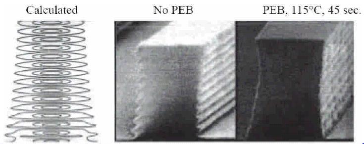
30 Substrate Preparation Pre-bake and Primer Vapor Primer STI Polysilicon P-Well USG Dehydration bake Remove moisture from wafer surface Promote adhesion between PR and surface Usually around 100 C Integration with primer coating Promotes adhesion of PR to wafer surface Widely used: Hexamethyldisilazane (HMDS) HMDS vapor coating prior to PR spin coating Usually performed in-situ with pre-bake Chill plate to cool down wafer before PR coating Dr. Ko, Institute of Nanotechnology, NCTU 30
31 Substrate Preparation Prep Chamber Primer Layer Wafer HMDS Vapor Wafer Hot Plate Dehydration Bake Hot Plate Primer Vapor Coating H 3 C H CH 3 Si Si 晶圓表面 H 3 C Si N Si CH 3 H 3 C CH 3 OH Si Si OH 親水性表面 H 3 C H 3C CH 3 CH 3 Si Si H 3 C CH 3 O O + H 2 O + NH 3 Si Si 疏水性表面 Dr. Ko, Institute of Nanotechnology, NCTU 31
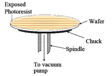
32 Resist Coating Primer STI Photoresist Polysilicon P-Well USG Wafer sits on a vacuum chuck Liquid photoresist applies at center of wafer Rotate at high speed Photoresist spreads by centrifugal force Evenly coat on wafer surface Dr. Ko, Institute of Nanotechnology, NCTU 32
33 Resist Spin Coater 33
34 Resist Thickness Viscosity Effect Dynamic Spin Rate Photoresist spread on spinning wafer surface Wafer held on a vacuum chuck Slow spin ~ 500 rpm Ramp up to ~ rpm 34
35 Resist Spin Coater 35
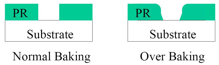
36 Soft Baking Hot plate heating is widely used Evaporating most of solvents from PR film (5~20 % left) Solvents help to make a thin PR but absorb radiation and affect adhesion Soft baking time and temperature are determined by the matrix evaluations Over bake: polymerized, less photo-sensitivity Under bake: affect adhesion and exposure (solvent is not sensitive) Dr. Ko, Institute of Nanotechnology, NCTU 36
37 Alignment & Exposure Gate Mask Gate Mask Photoresist Alignment and exposure Photoresist Polysilicon Polysilicon STI USG STI USG P-Well P-Well Alignment mark Most critical process for IC fabrication Most expensive tool (stepper or scanner) in an IC fab Most challenging technology Determines the minimum feature size Currently 65 nm and pushing to 45 nm Dr. Ko, Institute of Nanotechnology, NCTU 37

38 Structure of Mask Cr 2 O 3, 30nm Cr, 70nm quartz, 2.3mm Electron beam lithography Cr 2 O 3 Cr quartz Which illumination mode is correct? Dr. Ko, Institute of Nanotechnology, NCTU 38

39 Masks Bright field Dark field 39
40 Post Exposure Baking λ/2n PR Photoresist Photoresist STI Polysilicon P-Well USG Overexposure Underexposure Substrate Photoresist has glass transition temperature (T g ) Baking temperature higher than T g Thermal movement of photoresist molecules Rearrangement of the overexposed and underexposed PR molecules Average out standing wave effect Smooth PR sidewall and improve resolution Dr. Ko, Institute of Nanotechnology, NCTU 40
41 41
42 Development STI PR Polysilicon P-Well USG International standard of 2.38% TMAH (0.26 N) is used to reveal pattern Tetramethylammonium hydroxide, (CH 3 ) 4 NOH Developer solvent dissolves the softened part of photoresist Transferring the pattern from mask or reticle to photoresist Three basic steps: - Development -Rinse -Dry Dr. Ko, Institute of Nanotechnology, NCTU 42
43 43
44 Development 44
45 Hard Baking STI PR Polysilicon P-Well USG Dr. Ko, Institute of Nanotechnology, NCTU Evaporating all solvents in PR Improving etch and implantation resistance Improve PR adhesion with surface Polymerize and stabilize photoresist PR flow to fill pinhole Under-bake Photoresist is not fully polymerized High photoresist etch rate Poor adhesion Over-baking PR flow and bad resolution 45

46 Hard Baking 46
47 Pattern Inspection STI PR Polysilicon P-Well USG Inspection: go next step or rework (stripping PR) Photoresist pattern is temporary Etch or ion implantation pattern is permanent Photolithography process can rework Can t rework after etch or implantation Scanning electron microscope (SEM) Optical microscope (OM) Dr. Ko, Institute of Nanotechnology, NCTU 47
48 Pattern Inspection Overlay or alignment run-out, run-in, reticle rotation, wafer rotation, misplacement in X-direction, and misplacement in Y-direction Critical dimension (CD) Surface irregularities such as scratches, pin holes, stains, contamination, etc. 48


49 Critical Dimension (CD) Measurement In-line SEM plane-view inspection Off-line SEM cross-sectional inspection CD Atomic Force Microscope 49

50 Critical Dimension (CD) 50
51 Misalignment 51
Device Fabrication: Photolithography
 Device Fabrication: Photolithography 1 Objectives List the four components of the photoresist Describe the difference between +PR and PR Describe a photolithography process sequence List four alignment
Chapter 6. Photolithography
 Chapter 6 Photolithography 2006/4/10 1 Objectives List the four components of the photoresist Describe the difference between +PR and PR Describe a photolithography process sequence List four alignment
Chapter 6 Photolithography
 Chapter 6 Photolithography Hong Xiao, Ph. D. hxiao89@hotmail.com www2.austin.cc.tx.us/hongxiao/book.htm Hong Xiao, Ph. D. www2.austin.cc.tx.us/hongxiao/book.htm 1 Objectives List the four components of
Photolithography Technology and Application
 Photolithography Technology and Application Jeff Tsai Director, Graduate Institute of Electro-Optical Engineering Tatung University Art or Science? Lind width = 100 to 5 micron meter!! Resolution = ~ 3
Part 5-1: Lithography
 Part 5-1: Lithography Yao-Joe Yang 1 Pattern Transfer (Patterning) Types of lithography systems: Optical X-ray electron beam writer (non-traditional, no masks) Two-dimensional pattern transfer: limited
Major Fabrication Steps in MOS Process Flow
 Major Fabrication Steps in MOS Process Flow UV light Mask oxygen Silicon dioxide photoresist exposed photoresist oxide Silicon substrate Oxidation (Field oxide) Photoresist Coating Mask-Wafer Alignment
Photolithography I ( Part 1 )
") 1 Photolithography I ( Part 1 ) Chapter 13 : Semiconductor Manufacturing Technology by M. Quirk & J. Serda Bjørn-Ove Fimland, Department of Electronics and Telecommunication, Norwegian University of Science
1 Photolithography I ( Part 1 ) Chapter 13 : Semiconductor Manufacturing Technology by M. Quirk & J. Serda Bjørn-Ove Fimland, Department of Electronics and Telecommunication, Norwegian University of Science
Lecture 7. Lithography and Pattern Transfer. Reading: Chapter 7
 Lecture 7 Lithography and Pattern Transfer Reading: Chapter 7 Used for Pattern transfer into oxides, metals, semiconductors. 3 types of Photoresists (PR): Lithography and Photoresists 1.) Positive: PR
Lecture 13 Basic Photolithography
 Lecture 13 Basic Photolithography Chapter 12 Wolf and Tauber 1/64 Announcements Homework: Homework 3 is due today, please hand them in at the front. Will be returned one week from Thursday (16 th Nov).
Lithography. 3 rd. lecture: introduction. Prof. Yosi Shacham-Diamand. Fall 2004
 Lithography 3 rd lecture: introduction Prof. Yosi Shacham-Diamand Fall 2004 1 List of content Fundamental principles Characteristics parameters Exposure systems 2 Fundamental principles Aerial Image Exposure
Semiconductor Manufacturing Technology. Semiconductor Manufacturing Technology. Photolithography: Resist Development and Advanced Lithography
 Semiconductor Manufacturing Technology Michael Quirk & Julian Serda October 2001 by Prentice Hall Chapter 15 Photolithography: Resist Development and Advanced Lithography Eight Basic Steps of Photolithography
Section 2: Lithography. Jaeger Chapter 2 Litho Reader. The lithographic process
 Section 2: Lithography Jaeger Chapter 2 Litho Reader The lithographic process Photolithographic Process (a) (b) (c) (d) (e) (f) (g) Substrate covered with silicon dioxide barrier layer Positive photoresist
Section 2: Lithography. Jaeger Chapter 2 Litho Reader. EE143 Ali Javey Slide 5-1
 Section 2: Lithography Jaeger Chapter 2 Litho Reader EE143 Ali Javey Slide 5-1 The lithographic process EE143 Ali Javey Slide 5-2 Photolithographic Process (a) (b) (c) (d) (e) (f) (g) Substrate covered
Section 2: Lithography. Jaeger Chapter 2. EE143 Ali Javey Slide 5-1
 Section 2: Lithography Jaeger Chapter 2 EE143 Ali Javey Slide 5-1 The lithographic process EE143 Ali Javey Slide 5-2 Photolithographic Process (a) (b) (c) (d) (e) (f) (g) Substrate covered with silicon
Outline. 1 Introduction. 2 Basic IC fabrication processes. 3 Fabrication techniques for MEMS. 4 Applications. 5 Mechanics issues on MEMS MDL NTHU
 Outline 1 Introduction 2 Basic IC fabrication processes 3 Fabrication techniques for MEMS 4 Applications 5 Mechanics issues on MEMS 2.2 Lithography Reading: Runyan Chap. 5, or 莊達人 Chap. 7, or Wolf and
Module 11: Photolithography. Lecture 14: Photolithography 4 (Continued)
") Module 11: Photolithography Lecture 14: Photolithography 4 (Continued) 1 In the previous lecture, we have discussed the utility of the three printing modes, and their relative advantages and disadvantages.
Module 11: Photolithography Lecture 14: Photolithography 4 (Continued) 1 In the previous lecture, we have discussed the utility of the three printing modes, and their relative advantages and disadvantages.
EE 143 Microfabrication Technology Fall 2014
 EE 143 Microfabrication Technology Fall 2014 Prof. Clark T.-C. Nguyen Dept. of Electrical Engineering & Computer Sciences University of California at Berkeley Berkeley, CA 94720 EE 143: Microfabrication
Photolithography II ( Part 2 )
") 1 Photolithography II ( Part 2 ) Chapter 14 : Semiconductor Manufacturing Technology by M. Quirk & J. Serda Saroj Kumar Patra, Department of Electronics and Telecommunication, Norwegian University of Science
1 Photolithography II ( Part 2 ) Chapter 14 : Semiconductor Manufacturing Technology by M. Quirk & J. Serda Saroj Kumar Patra, Department of Electronics and Telecommunication, Norwegian University of Science
EE143 Fall 2016 Microfabrication Technologies. Lecture 3: Lithography Reading: Jaeger, Chap. 2
 EE143 Fall 2016 Microfabrication Technologies Lecture 3: Lithography Reading: Jaeger, Chap. 2 Prof. Ming C. Wu wu@eecs.berkeley.edu 511 Sutardja Dai Hall (SDH) 1-1 The lithographic process 1-2 1 Photolithographic
Dr. Dirk Meyners Prof. Wagner. Wagner / Meyners Micro / Nanosystems Technology
 Micro/Nanosystems Technology Dr. Dirk Meyners Prof. Wagner 1 Outline - Lithography Overview - UV-Lithography - Resolution Enhancement Techniques - Electron Beam Lithography - Patterning with Focused Ion
PHGN/CHEN/MLGN 435/535: Interdisciplinary Silicon Processing Laboratory. Simple Si solar Cell!
 Where were we? Simple Si solar Cell! Two Levels of Masks - photoresist, alignment Etch and oxidation to isolate thermal oxide, deposited oxide, wet etching, dry etching, isolation schemes Doping - diffusion/ion
5. Lithography. 1. photolithography intro: overall, clean room 2. principle 3. tools 4. pattern transfer 5. resolution 6. next-gen
 5. Lithography 1. photolithography intro: overall, clean room 2. principle 3. tools 4. pattern transfer 5. resolution 6. next-gen References: Semiconductor Devices: Physics and Technology. 2 nd Ed. SM
Semiconductor Technology
 Semiconductor Technology from A to Z + - x 1 0 x Photolithographie www.halbleiter.org Contents Contents List of Figures III 1 Photolithographie 1 1.1 Exposure and resist coating..........................
Photolithography. References: Introduction to Microlithography Thompson, Willson & Bowder, 1994
 Photolithography References: Introduction to Microlithography Thompson, Willson & Bowder, 1994 Microlithography, Science and Technology Sheats & Smith, 1998 Any other Microlithography or Photolithography
MICROCHIP MANUFACTURING by S. Wolf
 MICROCHIP MANUFACTURING by S. Wolf Chapter 19 LITHOGRAPHY II: IMAGE-FORMATION and OPTICAL HARDWARE 2004 by LATTICE PRESS CHAPTER 19 - CONTENTS Preliminaries: Wave- Motion & The Behavior of Light Resolution
Process Optimization
 Process Optimization Process Flow for non-critical layer optimization START Find the swing curve for the desired resist thickness. Determine the resist thickness (spin speed) from the swing curve and find
MICRO AND NANOPROCESSING TECHNOLOGIES
 MICRO AND NANOPROCESSING TECHNOLOGIES LECTURE 4 Optical lithography Concepts and processes Lithography systems Fundamental limitations and other issues Photoresists Photolithography process Process parameter
Micro/Nanolithography
 Dale E. Ewbank dale.ewbank@rit.edu unl081413_microe.ppt 2013 Dale E. Ewbank page 1 OUTLINE Masks Optical Lithography Photoresist Sensitivity Processing Exposure Tools Advanced Processes page 2 MICROLITHOGRAPHY
Lecture 8. Microlithography
 Lecture 8 Microlithography Lithography Introduction Process Flow Wafer Exposure Systems Masks Resists State of the Art Lithography Next Generation Lithography (NGL) Recommended videos: http://www.youtube.com/user/asmlcompany#p/search/1/jh6urfqt_d4
Optical Lithography. Keeho Kim Nano Team / R&D DongbuAnam Semi
 Optical Lithography Keeho Kim Nano Team / R&D DongbuAnam Semi Contents Lithography = Photolithography = Optical Lithography CD : Critical Dimension Resist Pattern after Development Exposure Contents Optical
Contrast Enhancement Materials CEM 365HR
 INTRODUCTION In 1989 Shin-Etsu Chemical acquired MicroSi, Inc. including their Contrast Enhancement Material (CEM) technology business*. A concentrated effort in the technology advancement of a CEM led
i- Line Photoresist Development: Replacement Evaluation of OiR
 i- Line Photoresist Development: Replacement Evaluation of OiR 906-12 Nishtha Bhatia High School Intern 31 July 2014 The Marvell Nanofabrication Laboratory s current i-line photoresist, OiR 897-10i, has
ECSE 6300 IC Fabrication Laboratory Lecture 3 Photolithography. Lecture Outline
 ECSE 6300 IC Fabrication Laboratory Lecture 3 Photolithography Prof. James J. Q. Lu Bldg. CII, Rooms 6229 Rensselaer Polytechnic Institute Troy, NY 12180 Tel. (518)276 2909 e mails: luj@rpi.edu http://www.ecse.rpi.edu/courses/s18/ecse
Module 11: Photolithography. Lecture11: Photolithography - I
 Module 11: Photolithography Lecture11: Photolithography - I 1 11.0 Photolithography Fundamentals We will all agree that incredible progress is happening in the filed of electronics and computers. For example,
Module - 2 Lecture - 13 Lithography I
 Nano Structured Materials-Synthesis, Properties, Self Assembly and Applications Prof. Ashok. K.Ganguli Department of Chemistry Indian Institute of Technology, Delhi Module - 2 Lecture - 13 Lithography
EE-527: MicroFabrication
 EE-57: MicroFabrication Exposure and Imaging Photons white light Hg arc lamp filtered Hg arc lamp excimer laser x-rays from synchrotron Electrons Ions Exposure Sources focused electron beam direct write
T in sec, I in W/cm 2, E in J/cm 2
 Exposures from Mask Aligner into Resist Mask aligner images created by shadowing from mask into resist Soft contact and Proximity good for 3 micron structures Vacuum Hard Contact: no shadow effects at
T in sec, I in W/cm 2, E in J/cm 2
 Exposures from Mask Aligner into Resist Mask aligner images created by shadowing from mask into resist Soft contact and Proximity good for 3 micron structures Vacuum Hard Contact: no shadow effects at
Clean Room Technology Optical Lithography. Lithography I. takenfrombdhuey
 Clean Room Technology Optical Lithography Lithography I If the automobile had followed the same development cycle as the computer, a Rolls Royce would today cost $100, get a million miles per gallon, and
Contrast Enhancement Materials CEM 365iS
 INTRODUCTION In 1989 Shin-Etsu Chemical acquired MicroSi, Inc. and the Contrast Enhancement Material (CEM) technology business from General Electric including a series of patents and technologies*. A concentrated
Microlithography. Dale E. Ewbank ul ppt. Microlithography Dale E. Ewbank page 1
 Dale E. Ewbank dale.ewbank@rit.edu ul012014.ppt 2014 Dale E. Ewbank page 1 OUTLINE Masks Optical Lithography Photoresist Sensitivity Processing Exposure Tools Advanced Processes page 2 MICROLITHOGRAPHY
3.Photolithography and resist systems
 3.Photolithography and resist systems Exposure Mercury arc lamp Shadow printing projection printing Photomask Substrates Resist systems DNQ-Novolak-based Epoxy-based Polyimide based 1 Exposure Mercury
Chapter 3 Fabrication
 Chapter 3 Fabrication The total structure of MO pick-up contains four parts: 1. A sub-micro aperture underneath the SIL The sub-micro aperture is used to limit the final spot size from 300nm to 600nm for
KMPR 1010 Process for Glass Wafers
 KMPR 1010 Process for Glass Wafers KMPR 1010 Steps Protocol Step System Condition Note Plasma Cleaning PVA Tepla Ion 10 5 mins Run OmniCoat Receipt Dehydration Any Heat Plate 150 C, 5 mins HMDS Coating
T in sec, I in W/cm 2, E in J/cm 2
 Exposures from Mask Aligner into Resist Mask aligner images created by shadowing from mask into resist Soft contact and Proximity good for 3 micron structures Vacuum Hard Contact: no shadow effects at
Chapter 3 Basics Semiconductor Devices and Processing
 Chapter 3 Basics Semiconductor Devices and Processing 1 Objectives Identify at least two semiconductor materials from the periodic table of elements List n-type and p-type dopants Describe a diode and
Lecture 5. Optical Lithography
 Lecture 5 Optical Lithography Intro For most of microfabrication purposes the process (e.g. additive, subtractive or implantation) has to be applied selectively to particular areas of the wafer: patterning
CMOS Digital Integrated Circuits Lec 2 Fabrication of MOSFETs
 CMOS Digital Integrated Circuits Lec 2 Fabrication of MOSFETs 1 CMOS Digital Integrated Circuits 3 rd Edition Categories of Materials Materials can be categorized into three main groups regarding their
Chapter 3: Basics Semiconductor Devices and Processing 2006/9/27 1. Topics
 Chapter 3: Basics Semiconductor Devices and Processing 2006/9/27 1 Topics What is semiconductor Basic semiconductor devices Basics of IC processing CMOS technologies 2006/9/27 2 1 What is Semiconductor
MICROLITHOGRAPHY 2004
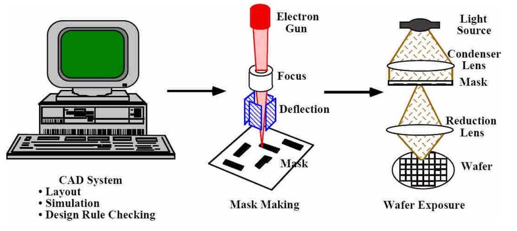
 MICROLITHOGRAPHY 2004 From Computer Aided Design (CAD) to Patterned Substrate At the CNF, a number of different options exist for producing a patterned substrate, but deciding which option is best for
Technology for the MEMS processing and testing environment. SUSS MicroTec AG Dr. Hans-Georg Kapitza
 Technology for the MEMS processing and testing environment SUSS MicroTec AG Dr. Hans-Georg Kapitza 1 SUSS MicroTec Industrial Group Founded 1949 as Karl Süss KG GmbH&Co. in Garching/ Munich San Jose Waterbury
CHAPTER 2 Principle and Design
 CHAPTER 2 Principle and Design The binary and gray-scale microlens will be designed and fabricated. Silicon nitride and photoresist will be taken as the material of the microlens in this thesis. The design
AZ 1512 RESIST PHOTOLITHOGRAPHY
 AZ 1512 RESIST PHOTOLITHOGRAPHY STANDARD OPERATIONAL PROCEDURE Faculty Supervisor: Prof. R. Bruce Darling Students: Katherine Lugo Danling Wang Department of Electrical Engineering Spring, 2009 TABLE OF
Update on 193nm immersion exposure tool
 Update on 193nm immersion exposure tool S. Owa, H. Nagasaka, Y. Ishii Nikon Corporation O. Hirakawa and T. Yamamoto Tokyo Electron Kyushu Ltd. January 28, 2004 Litho Forum 1 What is immersion lithography?
32nm High-K/Metal Gate Version Including 2nd Generation Intel Core processor family
 From Sand to Silicon Making of a Chip Illustrations 32nm High-K/Metal Gate Version Including 2nd Generation Intel Core processor family April 2011 1 The illustrations on the following foils are low resolution
Chapter 2 Silicon Planar Processing and Photolithography
 Chapter 2 Silicon Planar Processing and Photolithography The success of the electronics industry has been due in large part to advances in silicon integrated circuit (IC) technology based on planar processing,
From ArF Immersion to EUV Lithography
 From ArF Immersion to EUV Lithography Luc Van den hove Vice President IMEC Outline Introduction 193nm immersion lithography EUV lithography Global collaboration Conclusions Lithography is enabling 1000
(ksaligner & quintel resolution)
") Process [4.10] (ksaligner & quintel resolution) 1.0 Process Summary 1.1 Since Karl Suss ksaligner is heavily used and Quintel aligner is not, nanolab decided to compare the 2 micron line resolution from
Process [4.10] (ksaligner & quintel resolution) 1.0 Process Summary 1.1 Since Karl Suss ksaligner is heavily used and Quintel aligner is not, nanolab decided to compare the 2 micron line resolution from
MeRck. nlof 2000 Series. technical datasheet. Negative Tone Photoresists for Single Layer Lift-Off APPLICATION TYPICAL PROCESS
 MeRck technical datasheet AZ Negative Tone Photoresists for Single Layer Lift-Off APPLICATION AZ i-line photoresists are engineered to simplify the historically complex image reversal and multilayer lift-off
Institute of Solid State Physics. Technische Universität Graz. Lithography. Peter Hadley
 Technische Universität Graz Institute of Solid State Physics Lithography Peter Hadley http://www.cleanroom.byu.edu/virtual_cleanroom.parts/lithography.html http://www.cleanroom.byu.edu/su8.phtml Spin coater
Optical Requirements
 Optical Requirements Transmission vs. Film Thickness A pellicle needs a good light transmission and long term transmission stability. Transmission depends on the film thickness, film material and any anti-reflective
Photolithography Module
 Electronics Workforce Development System Photolithography Module Introduction Photolithography Module This module will teach students the different types of microlithographic systems being used today,
State-of-the-art device fabrication techniques
 State-of-the-art device fabrication techniques! Standard Photo-lithography and e-beam lithography! Advanced lithography techniques used in semiconductor industry Deposition: Thermal evaporation, e-gun
MeRck. AZ nlof technical datasheet. Negative Tone Photoresist for Single Layer Lift-Off APPLICATION TYPICAL PROCESS. SPIN CURVE (150MM Silicon)
") MeRck technical datasheet AZ nlof 5510 Negative Tone Photoresist for Single Layer Lift-Off APPLICATION AZ nlof 5510 i-line photoresist is engineered to simplify the historically complex image reversal
MeRck technical datasheet AZ nlof 5510 Negative Tone Photoresist for Single Layer Lift-Off APPLICATION AZ nlof 5510 i-line photoresist is engineered to simplify the historically complex image reversal
+ Preferred material for tool O Acceptable material for tool X Unacceptable material for tool
 Contact Aligners (HTG, ABM, EV620) GCA 5X g-line Stepper GCA i-line Steppers (GCA 10X, AS200) Shipley 1800 Series (1805, 1813, 1818, 1827) + + X AZ nlof 2000 O X + AZ4903 + + X OiR 620-7i X X + OiR 897-12i
Chapter 15 Summary and Future Trends
 Chapter 15 Summary and Future Trends Hong Xiao, Ph. D. hxiao89@hotmail.com www2.austin.cc.tx.us/hongxiao/book.htm Hong Xiao, Ph. D. www2.austin.cc.tx.us/hongxiao/book.htm 1 The 1960s First IC product Bipolar
College of Engineering Department of Electrical Engineering and Computer Sciences University of California, Berkeley
 College of Engineering Department of Electrical Engineering and Below are your weekly quizzes. You should print out a copy of the quiz and complete it before your lab section. Bring in the completed quiz
Microlithography. exposing radiation. mask. imaging system (low pass filter) photoresist. develop. etch
 photoresist. develop. etch") Microlithography Geometry Trends Master Patterns: Mask technology Pattern Transfer: Mask Aligner technology Wafer Transfer Media: Photo resist technology mask blank: transparent, mechanically rigid masking
Microlithography Geometry Trends Master Patterns: Mask technology Pattern Transfer: Mask Aligner technology Wafer Transfer Media: Photo resist technology mask blank: transparent, mechanically rigid masking
ADVANCED MASK MAKING AT RIT. David P. Kanen 5th Year Microelectronic Engineer Student Rochester Institute of Technology ABSTRACT
 ADVANCED MASK MAKING AT RIT David P. Kanen 5th Year Microelectronic Engineer Student Rochester Institute of Technology ABSTRACT This project involved the definition of the steps necessary to generate a
Optical Issues in Photolithography
 OpenStax-CNX module: m25448 1 Optical Issues in Photolithography Andrew R. Barron This work is produced by OpenStax-CNX and licensed under the Creative Commons Attribution License 3.0 note: This module
immersion optics Immersion Lithography with ASML HydroLith TWINSCAN System Modifications for Immersion Lithography by Bob Streefkerk
 immersion optics Immersion Lithography with ASML HydroLith by Bob Streefkerk For more than 25 years, many in the semiconductor industry have predicted the end of optical lithography. Recent developments,
Optical Lithography. Here Is Why. Burn J. Lin SPIE PRESS. Bellingham, Washington USA
 Optical Lithography Here Is Why Burn J. Lin SPIE PRESS Bellingham, Washington USA Contents Preface xiii Chapter 1 Introducing Optical Lithography /1 1.1 The Role of Lithography in Integrated Circuit Fabrication
450mm patterning out of darkness Backend Process Exposure Tool SOKUDO Lithography Breakfast Forum July 10, 2013 Doug Shelton Canon USA Inc.
 450mm patterning out of darkness Backend Process Exposure Tool SOKUDO Lithography Breakfast Forum 2013 July 10, 2013 Doug Shelton Canon USA Inc. Introduction Half Pitch [nm] 2013 2014 2015 2016 2017 2018
Micro- and Nano-Technology... for Optics
 Micro- and Nano-Technology...... for Optics 3.2 Lithography U.D. Zeitner Fraunhofer Institut für Angewandte Optik und Feinmechanik Jena Printing on Stones Map of Munich Stone Print Contact Printing light
FABRICATION OF CMOS INTEGRATED CIRCUITS. Dr. Mohammed M. Farag
 FABRICATION OF CMOS INTEGRATED CIRCUITS Dr. Mohammed M. Farag Outline Overview of CMOS Fabrication Processes The CMOS Fabrication Process Flow Design Rules Reference: Uyemura, John P. "Introduction to
(a) (d) (e) (b) (c) (f) 3D-NAND Flash and Its Manufacturing Process
 (d) (e) (b) (c) (f) 3D-NAND Flash and Its Manufacturing Process") 3D-NAND Flash and Its Manufacturing Process 79 (d) Si Si (b) (c) (e) Si (f) +1-2 (g) (h) Figure 2.33 Top-down view in cap oxide and (b) in nitride_n-2; (c) cross-section near the top of the channel; top-down
3D-NAND Flash and Its Manufacturing Process 79 (d) Si Si (b) (c) (e) Si (f) +1-2 (g) (h) Figure 2.33 Top-down view in cap oxide and (b) in nitride_n-2; (c) cross-section near the top of the channel; top-down
Lithography. Development of High-Quality Attenuated Phase-Shift Masks
 Lithography S P E C I A L Development of High-Quality Attenuated Phase-Shift Masks by Toshihiro Ii and Masao Otaki, Toppan Printing Co., Ltd. Along with the year-by-year acceleration of semiconductor device
MICROBUMP CREATION SYSTEM FOR ADVANCED PACKAGING APPLICATIONS
 MICROBUMP CREATION SYSTEM FOR ADVANCED PACKAGING APPLICATIONS Andrew Ahr, EKC Technology, & Chester E. Balut, DuPont Electronic Technologies Alan Huffman, RTI International Abstract Today, the electronics
Photoresist Absorbance and Bleaching Laboratory
 MCEE 505 Lithography Materials and Processes Page 1 of 5 Photoresist Absorbance and Bleaching Laboratory Microelectronic Engineering Rochester Institute of Technology 1. OBJECTIVE The objective of this
From Sand to Silicon Making of a Chip Illustrations May 2009
 From Sand to Silicon Making of a Chip Illustrations May 2009 1 The illustrations on the following foils are low resolution images that visually support the explanations of the individual steps. For publishing
Micro- and Nano- Fabrication and Replication Techniques
 Micro- and Nano- Fabrication and Replication Techniques Why do we have to write thing small and replicate fast? Plenty of Room at the Bottom Richard P. Feynman, December 1959 How do we write it? We have
Photolithography 光刻 Part I: Optics
 微纳光电子材料与器件工艺原理 Photolithography 光刻 Part I: Optics Xing Sheng 盛兴 Department of Electronic Engineering Tsinghua University xingsheng@tsinghua.edu.cn 1 Integrate Circuits Moore's law transistor number transistor
Micro- and Nano-Technology... for Optics
 Micro- and Nano-Technology...... for Optics 3.2 Lithography U.D. Zeitner Fraunhofer Institut für Angewandte Optik und Feinmechanik Jena Printing on Stones Map of Munich Stone Print Shadow Printing Photomask
2.1 BASIC THEORY: INTERFERENCE OF TWO BEAMS
 2 LASER INTERFERENCE LITHOGRAPHY (LIL) 9 2 LASER INTERFERENCE LITHOGRAPHY (LIL) Laser interference lithography [3~22] (LIL) is a method to produce periodic structures using two interfering highly-coherent
CHAPTER TWO METALLOGRAPHY & MICROSCOPY
 CHAPTER TWO METALLOGRAPHY & MICROSCOPY 1. INTRODUCTION: Materials characterisation has two main aspects: Accurately measuring the physical, mechanical and chemical properties of materials Accurately measuring
DOE Project: Resist Characterization
 DOE Project: Resist Characterization GOAL To achieve high resolution and adequate throughput, a photoresist must possess relatively high contrast and sensitivity to exposing radiation. The objective of
Forming a vertical interconnect structure using dry film processing for Fan Out Wafer Level Packaging
 2017 IEEE 67th Electronic Components and Technology Conference Forming a vertical interconnect structure using dry film processing for Fan Out Wafer Level Packaging Yew Wing Leong, Hsiang Yao Hsiao, Soon
William Reiniach 5th Year Microelectronic Engineering Student Rochester Institute of Technology
 DEVELOPMENT OF A PHOTOSENSITIVE POLYIMIDE PROCESS William Reiniach 5th Year Microelectronic Engineering Student Rochester Institute of Technology 1~BS TRACT A six step lithographic process has been developed
BI-LAYER DEEP UV RESIST SYSTEM. Mark A. Boehm 5th Year Microelectronic Engineering Student Rochester Institute of Technology ABSTRACT
 INTRODUCTION BI-LAYER DEEP UV RESIST SYSTEM Mark A. Boehm 5th Year Microelectronic Engineering Student Rochester Institute of Technology ABSTRACT A portable conformable mask (PCM) system employing KTIS2O
THE USE OF A CONTRAST ENHANCEMENT LAYER TO EXTEND THE PRACTICAL RESOLUTION LIMITS OF OPTICAL LITHOGRAPHIC SYSTEMS
 THE USE OF A CONTRAST ENHANCEMENT LAYER TO EXTEND THE PRACTICAL RESOLUTION LIMITS OF OPTICAL LITHOGRAPHIC SYSTEMS Daniel R. Sutton 5th Year Microelectronic Engineering Student Rochester Institute of Technology
Nanoscale Lithography. NA & Immersion. Trends in λ, NA, k 1. Pushing The Limits of Photolithography Introduction to Nanotechnology
 15-398 Introduction to Nanotechnology Nanoscale Lithography Seth Copen Goldstein Seth@cs.cmu.Edu CMU Pushing The Limits of Photolithography Reduce wavelength (λ) Use Reducing Lens Increase Numerical Aperture
Optolith 2D Lithography Simulator
 2D Lithography Simulator Advanced 2D Optical Lithography Simulator 4/13/05 Introduction is a powerful non-planar 2D lithography simulator that models all aspects of modern deep sub-micron lithography It
Holistic View of Lithography for Double Patterning. Skip Miller ASML
 Holistic View of Lithography for Double Patterning Skip Miller ASML Outline Lithography Requirements ASML Holistic Lithography Solutions Conclusions Slide 2 Shrink Continues Lithography keeps adding value
UV Nanoimprint Stepper Technology: Status and Roadmap. S.V. Sreenivasan Sematech Litho Forum May 14 th, 2008
 UV Nanoimprint Stepper Technology: Status and Roadmap S.V. Sreenivasan Sematech Litho Forum May 14 th, 2008 Overview Introduction Stepper technology status: Patterning and CD Control Through Etch Alignment
Surface Topography and Alignment Effects in UV-Modified Polyimide Films with Micron Size Patterns
 CHINESE JOURNAL OF PHYSICS VOL. 41, NO. 2 APRIL 2003 Surface Topography and Alignment Effects in UV-Modified Polyimide Films with Micron Size Patterns Ru-Pin Pan 1, Hua-Yu Chiu 1,Yea-FengLin 1,andJ.Y.Huang
2 Integrated Circuit Manufacturing:
 2 Integrated Circuit Manufacturing: A Technology Resource 2 IC MANUFACTURING TECHNOLOGIES While the integrated circuit drives the packaging and assembly, the IC manufacturing process, and associated methodologies,
DIY fabrication of microstructures by projection photolithography
 DIY fabrication of microstructures by projection photolithography Andrew Zonenberg Rensselaer Polytechnic Institute 110 8th Street Troy, New York U.S.A. 12180 zonena@cs.rpi.edu April 20, 2011 Abstract
EG2605 Undergraduate Research Opportunities Program. Large Scale Nano Fabrication via Proton Lithography Using Metallic Stencils
 EG2605 Undergraduate Research Opportunities Program Large Scale Nano Fabrication via Proton Lithography Using Metallic Stencils Tan Chuan Fu 1, Jeroen Anton van Kan 2, Pattabiraman Santhana Raman 2, Yao
2009 International Workshop on EUV Lithography
 Contents Introduction Absorber Stack Optimization Non-flatness Correction Blank Defect and Its Mitigation Wafer Printing Inspection Actinic Metrology Cleaning and Repair Status Remaining Issues in EUV
UV LED ILLUMINATION STEPPER OFFERS HIGH PERFORMANCE AND LOW COST OF OWNERSHIP
 UV LED ILLUMINATION STEPPER OFFERS HIGH PERFORMANCE AND LOW COST OF OWNERSHIP Casey Donaher, Rudolph Technologies Herbert J. Thompson, Rudolph Technologies Chin Tiong Sim, Rudolph Technologies Rudolph