3.Photolithography and resist systems
|
|
|
- Branden Gaines
- 6 years ago
- Views:
Transcription
1 3.Photolithography and resist systems Exposure Mercury arc lamp Shadow printing projection printing Photomask Substrates Resist systems DNQ-Novolak-based Epoxy-based Polyimide based 1 Exposure Mercury arc spectrum (total power emission: 100 to 2000 W) 405 nm 365 nm 436 nm Broad emission (depending on exposure tool) Single emission lines g-line 436 nm h-line 405 nm i-line 365 nm each line contains less than 2 % of the total power of the lamp 2
![Exposure Maskaligner MA6 [SÜSS] No.](/docs-images/75/72669926/images/2-0.jpg "2: Hg-lamp No.")


2 Exposure Maskaligner MA6 [SÜSS] No. 2: Hg-lamp No. 3-12: mirrors, lenses No. 13: mask No. 14: wafer 3 Exposure and Alignment Hint for first level: Align to Flat! Top Side Alignment Back Side Alignment [SÜSS] 4

![b min 3 µm Contact: gapd prox = 0 b min 0,7µm [SZE03] * assumed: reproduction of a grating with equal width lines and spaces 5 Resolution of Shadow Printing](/docs-images/75/72669926/images/3-1.jpg "Reduce λ b min = k λ d prox Reduce d prox tre + 2 sist Reduce t Resist Reduce k Ways to improve resolution Achievable resolution (dependent on process conditions)")
3 Resolution of Shadow Printing Minimum printable linewidth b min *: b min = k λ d prox + t Re sist 2 Contact and proximity printing λ exposure wavelength d gap between mask and photoresist t photoresist thickness k variable factor, depending on process Example: λ = 436nm, t Resist = 2µm; k=1 Proximity: gapd prox = 20µm; b min 3 µm Contact: gapd prox = 0 b min 0,7µm [SZE03] * assumed: reproduction of a grating with equal width lines and spaces 5 Resolution of Shadow Printing Reduce λ b min = k λ d prox Reduce d prox tre + 2 sist Reduce t Resist Reduce k Ways to improve resolution Achievable resolution (dependent on process conditions) [Süss] 6
4 Resolution of Projection Printing Numerical aperture NA NA = n sin θ = D / 2f f: focal length D: lens diameter n: refractive index for the medium Theoretical resolution W of a lens[1] W = k 1 λ/na λ: exposure wavelength k: empirically determined, process dependent varies from 0.3 to 1.1 k = 0.75 for single layer resists k = 1.1 for resists over reflective surfaces like Aluminium [More88] Depth of focus DOF DOF = k 2 λ/2(na) 2 [1] Rayleigh limit for two opaque objects 7 Resolution of Projection Printing Reduce λ W = k λ/na IncreaseNA NA = n sin θ = D / 2f Reduce k Increase refractive index for the medium* Ways to improve resolution Numerical Aperture (NA) Theoretical resolution (W) for k = 0.75 Depth of focus (DOF) λ = 400 nm λ = 200 nm λ = 400 nm λ = 200 nm μm 0.8 μm 5.0 μm 2.5 μm Achievable resolution (dependent on process conditions) μm 0.5 μm 2.0 μm 1.0 μm μm 0.4 μm 1.5 μm 0.8 μm μm 0.3 μm 0.8 μm 0.4 μm *NA 0,85 immersion lithography 8


5 Photomask Material transparency Absorption layer Structure resolutions sodalime, quarz-glas; polymer chromium; ink laser, e-beam; photoplotter Mask Polarity Shadow mask 5 x 5 inches square, sodalime/chromium Quarz-glas low coefficient of thermal expansion transparent in the deep UV [Wolf86] 9 Substrates Silicon Wafer Material Format Flatness Roughness Adhesion 300 mm 10
6 Resist Systems Important Resist Types for Photolithography DNQ-Novolak-based Epoxy-based Polyimide-based Positive tone Negative tone Image Reversal Negative tone Negative tone Positive tone Some trade names: ma-p, AR-P, AZ Some trade names: ma-n, AR-N, TI Some trade names: AZ..E, TI..XR Some trade names: SU-8, GM Some trade names: Durimid Some trade names: HD Resist Systems DNQ-Novolak-based positive tone Epoxy-based negative tone Polyimide-based negative tone resin PAC* solvent Novolak DNQ-sulfonates Organic solvent (PGMEA) Epoxy resin Organic salt Organic solvent (e.g. γ-bytyrolactone and propylene carbonate) Photoactive precursor (polyamic acids/esters) organic solvents main effect of exposure change of molecular structure of DNQ and post exposure bake: crosslinking of epoxy resin imidisation crosslinked intermediate developer aqueous alkaline solvent organic solvent (e.g. PGMEA = safer solvent) organic or aqueous solvent (denpending on resist) hardbake optional optional (= curing) completing imidisation polyimide stripping concentrated developer; acetone PG remover, RIE plasma ashing, laser ablation,... plasma ashing... * PAC = photoactive compound 12


7 Resist Systems Some Applications DNQ-Novolak-based Epoxy-based Polyimide-based Masking for processes Wet etching Dry etching Electroplating Lift off process Micromechanical devices Masking for processes Electroplating (UV-)LIGA Lift off process Stress buffer Passivation layer Dielectric interlayer (multichip module) Coatings for optic fiber and quartz capillary coatings Masking for processes Dry etch mask for silicon nitride passivation layer 13 DNQ-Novolak-based resists Resist Chemistry Resist: Interaction beween novolak and DNQ: hydrogen bonds Resin: phenol novolak PAC: DNQ-Sulfonate DNQ photolysis: Dissolution rate scheme: fhgfhfghfhfhhhhhhhhhhhhhhhhhhhhhhhhhhhhhhhh hhhhhhhhhhhhhhhhhhhhhhhhhhhhhhhhhhhhhhhh hhhhhklklllllllllllllllllllllllllllllllllllllllllllllllllllll [Damm93] 14


8 Mesomerie der Carboxylgruppe: als Tafelbild 15 DNQ-Novolak-based resists fhgfhfghfhfhhhhhhhhhhhhhhhhhhhhhh hhhhhhhhhhhhhhhhhhhhhhhhhhhhhhh hhhhhhhhhhhhhhhhhhhhhhhhklklllllllllll lllllllllllllllllllllllllllllllllllllllll Dissolution rates of unexposed and fully exposed mixtures of DNQ and novolak Absorption spectra of DNQ-based photosensitizers before and after bleaching [Damm93] 16
9 DNQ-Novolak-based resists [micro04] Clariant AZ and MicroChemicals TI resists 17 DNQ-Novolak-based resists: positive tone Two layer process [Roth99] 18
10 Erklärung der Ursachen eines typischen Resistprofils für DNQ-Novolak-Resiste: als Tafelbild 19 DNQ-Novolak-based resists: image reversal Goal of image reversal: enhance the process latitude Most important principles: indirect (base-catalysed) direct (acid-catalysed) HO-A-OH: bifunctional, acid-captivated crosslinker Dissolution rate scheme Principle of direct image reversal 20
 21")

11 Unterschied belichtete und unbelichtete Bereiche im säurekatalysierten Umkehrresist: Belichter Resist Unbelichter Resist Vernetzende Substanz Temperatur Katalysator (Säure) 21 Epoxy-based resist Resist Chemistry photosensitiver epoxy resin Photochemical reaction: crosslinking Frage: Säure HA ist ein kleines Molekül. Was bedeutet das für die Vernetzung? [Lee95, Micro01] 22

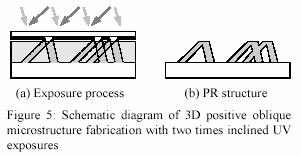
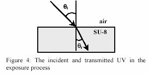
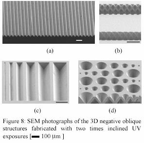
12 Epoxy-based resist Inclined/rotated exposure of SU-8 [Manh03] 23 Polyimide-based resists Chemical Principle and Processing Scheme (Starting from polyamic acid methacrylate ester) Nachteil? [Ahne95] 24
Section 2: Lithography. Jaeger Chapter 2. EE143 Ali Javey Slide 5-1
 Section 2: Lithography Jaeger Chapter 2 EE143 Ali Javey Slide 5-1 The lithographic process EE143 Ali Javey Slide 5-2 Photolithographic Process (a) (b) (c) (d) (e) (f) (g) Substrate covered with silicon
Dr. Dirk Meyners Prof. Wagner. Wagner / Meyners Micro / Nanosystems Technology
 Micro/Nanosystems Technology Dr. Dirk Meyners Prof. Wagner 1 Outline - Lithography Overview - UV-Lithography - Resolution Enhancement Techniques - Electron Beam Lithography - Patterning with Focused Ion
Part 5-1: Lithography
 Part 5-1: Lithography Yao-Joe Yang 1 Pattern Transfer (Patterning) Types of lithography systems: Optical X-ray electron beam writer (non-traditional, no masks) Two-dimensional pattern transfer: limited
Module 11: Photolithography. Lecture 14: Photolithography 4 (Continued)
") Module 11: Photolithography Lecture 14: Photolithography 4 (Continued) 1 In the previous lecture, we have discussed the utility of the three printing modes, and their relative advantages and disadvantages.
Module 11: Photolithography Lecture 14: Photolithography 4 (Continued) 1 In the previous lecture, we have discussed the utility of the three printing modes, and their relative advantages and disadvantages.
Section 2: Lithography. Jaeger Chapter 2 Litho Reader. The lithographic process
 Section 2: Lithography Jaeger Chapter 2 Litho Reader The lithographic process Photolithographic Process (a) (b) (c) (d) (e) (f) (g) Substrate covered with silicon dioxide barrier layer Positive photoresist
Section 2: Lithography. Jaeger Chapter 2 Litho Reader. EE143 Ali Javey Slide 5-1
 Section 2: Lithography Jaeger Chapter 2 Litho Reader EE143 Ali Javey Slide 5-1 The lithographic process EE143 Ali Javey Slide 5-2 Photolithographic Process (a) (b) (c) (d) (e) (f) (g) Substrate covered
Major Fabrication Steps in MOS Process Flow
 Major Fabrication Steps in MOS Process Flow UV light Mask oxygen Silicon dioxide photoresist exposed photoresist oxide Silicon substrate Oxidation (Field oxide) Photoresist Coating Mask-Wafer Alignment
Lithography. 3 rd. lecture: introduction. Prof. Yosi Shacham-Diamand. Fall 2004
 Lithography 3 rd lecture: introduction Prof. Yosi Shacham-Diamand Fall 2004 1 List of content Fundamental principles Characteristics parameters Exposure systems 2 Fundamental principles Aerial Image Exposure
Semiconductor Manufacturing Technology. Semiconductor Manufacturing Technology. Photolithography: Resist Development and Advanced Lithography
 Semiconductor Manufacturing Technology Michael Quirk & Julian Serda October 2001 by Prentice Hall Chapter 15 Photolithography: Resist Development and Advanced Lithography Eight Basic Steps of Photolithography
EE143 Fall 2016 Microfabrication Technologies. Lecture 3: Lithography Reading: Jaeger, Chap. 2
 EE143 Fall 2016 Microfabrication Technologies Lecture 3: Lithography Reading: Jaeger, Chap. 2 Prof. Ming C. Wu wu@eecs.berkeley.edu 511 Sutardja Dai Hall (SDH) 1-1 The lithographic process 1-2 1 Photolithographic
Photolithography I ( Part 1 )
") 1 Photolithography I ( Part 1 ) Chapter 13 : Semiconductor Manufacturing Technology by M. Quirk & J. Serda Bjørn-Ove Fimland, Department of Electronics and Telecommunication, Norwegian University of Science
1 Photolithography I ( Part 1 ) Chapter 13 : Semiconductor Manufacturing Technology by M. Quirk & J. Serda Bjørn-Ove Fimland, Department of Electronics and Telecommunication, Norwegian University of Science
Lecture 7. Lithography and Pattern Transfer. Reading: Chapter 7
 Lecture 7 Lithography and Pattern Transfer Reading: Chapter 7 Used for Pattern transfer into oxides, metals, semiconductors. 3 types of Photoresists (PR): Lithography and Photoresists 1.) Positive: PR
Lecture 13 Basic Photolithography
 Lecture 13 Basic Photolithography Chapter 12 Wolf and Tauber 1/64 Announcements Homework: Homework 3 is due today, please hand them in at the front. Will be returned one week from Thursday (16 th Nov).
MICRO AND NANOPROCESSING TECHNOLOGIES
 MICRO AND NANOPROCESSING TECHNOLOGIES LECTURE 4 Optical lithography Concepts and processes Lithography systems Fundamental limitations and other issues Photoresists Photolithography process Process parameter
PHGN/CHEN/MLGN 435/535: Interdisciplinary Silicon Processing Laboratory. Simple Si solar Cell!
 Where were we? Simple Si solar Cell! Two Levels of Masks - photoresist, alignment Etch and oxidation to isolate thermal oxide, deposited oxide, wet etching, dry etching, isolation schemes Doping - diffusion/ion
Lithography Is the Designer s Brush. Lithography is indispensible for defining locations and configurations of circuit elements/functions.
 Lithography 1 Lithography Is the Designer s Brush Lithography is indispensible for defining locations and configurations of circuit elements/functions. 2 ITRS 2007 The major challenge in litho: CD, CD
Photolithography II ( Part 2 )
") 1 Photolithography II ( Part 2 ) Chapter 14 : Semiconductor Manufacturing Technology by M. Quirk & J. Serda Saroj Kumar Patra, Department of Electronics and Telecommunication, Norwegian University of Science
1 Photolithography II ( Part 2 ) Chapter 14 : Semiconductor Manufacturing Technology by M. Quirk & J. Serda Saroj Kumar Patra, Department of Electronics and Telecommunication, Norwegian University of Science
EE-527: MicroFabrication
 EE-57: MicroFabrication Exposure and Imaging Photons white light Hg arc lamp filtered Hg arc lamp excimer laser x-rays from synchrotron Electrons Ions Exposure Sources focused electron beam direct write
Clean Room Technology Optical Lithography. Lithography I. takenfrombdhuey
 Clean Room Technology Optical Lithography Lithography I If the automobile had followed the same development cycle as the computer, a Rolls Royce would today cost $100, get a million miles per gallon, and
CHAPTER 2 Principle and Design
 CHAPTER 2 Principle and Design The binary and gray-scale microlens will be designed and fabricated. Silicon nitride and photoresist will be taken as the material of the microlens in this thesis. The design
Module 11: Photolithography. Lecture11: Photolithography - I
 Module 11: Photolithography Lecture11: Photolithography - I 1 11.0 Photolithography Fundamentals We will all agree that incredible progress is happening in the filed of electronics and computers. For example,
Micro- and Nano-Technology... for Optics
 Micro- and Nano-Technology...... for Optics 3.2 Lithography U.D. Zeitner Fraunhofer Institut für Angewandte Optik und Feinmechanik Jena Printing on Stones Map of Munich Stone Print Shadow Printing Photomask
EE 143 Microfabrication Technology Fall 2014
 EE 143 Microfabrication Technology Fall 2014 Prof. Clark T.-C. Nguyen Dept. of Electrical Engineering & Computer Sciences University of California at Berkeley Berkeley, CA 94720 EE 143: Microfabrication
MICROCHIP MANUFACTURING by S. Wolf
 MICROCHIP MANUFACTURING by S. Wolf Chapter 19 LITHOGRAPHY II: IMAGE-FORMATION and OPTICAL HARDWARE 2004 by LATTICE PRESS CHAPTER 19 - CONTENTS Preliminaries: Wave- Motion & The Behavior of Light Resolution
Micro- and Nano-Technology... for Optics
 Micro- and Nano-Technology...... for Optics 3.2 Lithography U.D. Zeitner Fraunhofer Institut für Angewandte Optik und Feinmechanik Jena Printing on Stones Map of Munich Stone Print Contact Printing light
Photolithography. References: Introduction to Microlithography Thompson, Willson & Bowder, 1994
 Photolithography References: Introduction to Microlithography Thompson, Willson & Bowder, 1994 Microlithography, Science and Technology Sheats & Smith, 1998 Any other Microlithography or Photolithography
Outline. 1 Introduction. 2 Basic IC fabrication processes. 3 Fabrication techniques for MEMS. 4 Applications. 5 Mechanics issues on MEMS MDL NTHU
 Outline 1 Introduction 2 Basic IC fabrication processes 3 Fabrication techniques for MEMS 4 Applications 5 Mechanics issues on MEMS 2.2 Lithography Reading: Runyan Chap. 5, or 莊達人 Chap. 7, or Wolf and
Chapter 3 Fabrication
 Chapter 3 Fabrication The total structure of MO pick-up contains four parts: 1. A sub-micro aperture underneath the SIL The sub-micro aperture is used to limit the final spot size from 300nm to 600nm for
Lecture 8. Microlithography
 Lecture 8 Microlithography Lithography Introduction Process Flow Wafer Exposure Systems Masks Resists State of the Art Lithography Next Generation Lithography (NGL) Recommended videos: http://www.youtube.com/user/asmlcompany#p/search/1/jh6urfqt_d4
Lecture 22 Optical MEMS (4)
") EEL6935 Advanced MEMS (Spring 2005) Instructor: Dr. Huikai Xie Lecture 22 Optical MEMS (4) Agenda: Refractive Optical Elements Microlenses GRIN Lenses Microprisms Reference: S. Sinzinger and J. Jahns,
EEL6935 Advanced MEMS (Spring 2005) Instructor: Dr. Huikai Xie Lecture 22 Optical MEMS (4) Agenda: Refractive Optical Elements Microlenses GRIN Lenses Microprisms Reference: S. Sinzinger and J. Jahns,
Micro/Nanolithography
 Dale E. Ewbank dale.ewbank@rit.edu unl081413_microe.ppt 2013 Dale E. Ewbank page 1 OUTLINE Masks Optical Lithography Photoresist Sensitivity Processing Exposure Tools Advanced Processes page 2 MICROLITHOGRAPHY
Radial Coupling Method for Orthogonal Concentration within Planar Micro-Optic Solar Collectors
 Radial Coupling Method for Orthogonal Concentration within Planar Micro-Optic Solar Collectors Jason H. Karp, Eric J. Tremblay and Joseph E. Ford Photonics Systems Integration Lab University of California
Module - 2 Lecture - 13 Lithography I
 Nano Structured Materials-Synthesis, Properties, Self Assembly and Applications Prof. Ashok. K.Ganguli Department of Chemistry Indian Institute of Technology, Delhi Module - 2 Lecture - 13 Lithography
+ Preferred material for tool O Acceptable material for tool X Unacceptable material for tool
 Contact Aligners (HTG, ABM, EV620) GCA 5X g-line Stepper GCA i-line Steppers (GCA 10X, AS200) Shipley 1800 Series (1805, 1813, 1818, 1827) + + X AZ nlof 2000 O X + AZ4903 + + X OiR 620-7i X X + OiR 897-12i
Fabrication Techniques of Optical ICs
 Fabrication Techniques of Optical ICs Processing Techniques Lift off Process Etching Process Patterning Techniques Photo Lithography Electron Beam Lithography Photo Resist ( Microposit MP1300) Electron
This writeup is adapted from Fall 2002, final project report for by Robert Winsor.
 Optical Waveguides in Andreas G. Andreou This writeup is adapted from Fall 2002, final project report for 520.773 by Robert Winsor. September, 2003 ABSTRACT This lab course is intended to give students
Figure 7 Dynamic range expansion of Shack- Hartmann sensor using a spatial-light modulator
 Figure 4 Advantage of having smaller focal spot on CCD with super-fine pixels: Larger focal point compromises the sensitivity, spatial resolution, and accuracy. Figure 1 Typical microlens array for Shack-Hartmann
Optical Requirements
 Optical Requirements Transmission vs. Film Thickness A pellicle needs a good light transmission and long term transmission stability. Transmission depends on the film thickness, film material and any anti-reflective
EG2605 Undergraduate Research Opportunities Program. Large Scale Nano Fabrication via Proton Lithography Using Metallic Stencils
 EG2605 Undergraduate Research Opportunities Program Large Scale Nano Fabrication via Proton Lithography Using Metallic Stencils Tan Chuan Fu 1, Jeroen Anton van Kan 2, Pattabiraman Santhana Raman 2, Yao
Optical Issues in Photolithography
 OpenStax-CNX module: m25448 1 Optical Issues in Photolithography Andrew R. Barron This work is produced by OpenStax-CNX and licensed under the Creative Commons Attribution License 3.0 note: This module
Optical Lithography. Keeho Kim Nano Team / R&D DongbuAnam Semi
 Optical Lithography Keeho Kim Nano Team / R&D DongbuAnam Semi Contents Lithography = Photolithography = Optical Lithography CD : Critical Dimension Resist Pattern after Development Exposure Contents Optical
Photolithography 光刻 Part I: Optics
 微纳光电子材料与器件工艺原理 Photolithography 光刻 Part I: Optics Xing Sheng 盛兴 Department of Electronic Engineering Tsinghua University xingsheng@tsinghua.edu.cn 1 Integrate Circuits Moore's law transistor number transistor
Integrated Focusing Photoresist Microlenses on AlGaAs Top-Emitting VCSELs
 Integrated Focusing Photoresist Microlenses on AlGaAs Top-Emitting VCSELs Andrea Kroner We present 85 nm wavelength top-emitting vertical-cavity surface-emitting lasers (VCSELs) with integrated photoresist
Microlithography. Dale E. Ewbank ul ppt. Microlithography Dale E. Ewbank page 1
 Dale E. Ewbank dale.ewbank@rit.edu ul012014.ppt 2014 Dale E. Ewbank page 1 OUTLINE Masks Optical Lithography Photoresist Sensitivity Processing Exposure Tools Advanced Processes page 2 MICROLITHOGRAPHY
State-of-the-art device fabrication techniques
 State-of-the-art device fabrication techniques! Standard Photo-lithography and e-beam lithography! Advanced lithography techniques used in semiconductor industry Deposition: Thermal evaporation, e-gun
Microlithography. exposing radiation. mask. imaging system (low pass filter) photoresist. develop. etch
 photoresist. develop. etch") Microlithography Geometry Trends Master Patterns: Mask technology Pattern Transfer: Mask Aligner technology Wafer Transfer Media: Photo resist technology mask blank: transparent, mechanically rigid masking
Microlithography Geometry Trends Master Patterns: Mask technology Pattern Transfer: Mask Aligner technology Wafer Transfer Media: Photo resist technology mask blank: transparent, mechanically rigid masking
Contrast Enhancement Materials CEM 365HR
 INTRODUCTION In 1989 Shin-Etsu Chemical acquired MicroSi, Inc. including their Contrast Enhancement Material (CEM) technology business*. A concentrated effort in the technology advancement of a CEM led
Device Fabrication: Photolithography
 Device Fabrication: Photolithography 1 Objectives List the four components of the photoresist Describe the difference between +PR and PR Describe a photolithography process sequence List four alignment
Optical Lithography. Here Is Why. Burn J. Lin SPIE PRESS. Bellingham, Washington USA
 Optical Lithography Here Is Why Burn J. Lin SPIE PRESS Bellingham, Washington USA Contents Preface xiii Chapter 1 Introducing Optical Lithography /1 1.1 The Role of Lithography in Integrated Circuit Fabrication
Innovative Mask Aligner Lithography for MEMS and Packaging
 Innovative Mask Aligner Lithography for MEMS and Packaging Dr. Reinhard Voelkel CEO SUSS MicroOptics SA September 9 th, 2010 1 SUSS Micro-Optics SUSS MicroOptics is a leading supplier for high-quality
MICROLITHOGRAPHY 2004
 MICROLITHOGRAPHY 2004 From Computer Aided Design (CAD) to Patterned Substrate At the CNF, a number of different options exist for producing a patterned substrate, but deciding which option is best for
Contrast Enhancement Materials CEM 365iS
 INTRODUCTION In 1989 Shin-Etsu Chemical acquired MicroSi, Inc. and the Contrast Enhancement Material (CEM) technology business from General Electric including a series of patents and technologies*. A concentrated
OPTI510R: Photonics. Khanh Kieu College of Optical Sciences, University of Arizona Meinel building R.626
 OPTI510R: Photonics Khanh Kieu College of Optical Sciences, University of Arizona kkieu@optics.arizona.edu Meinel building R.626 Announcements Homework #3 is due today No class Monday, Feb 26 Pre-record
William Reiniach 5th Year Microelectronic Engineering Student Rochester Institute of Technology
 DEVELOPMENT OF A PHOTOSENSITIVE POLYIMIDE PROCESS William Reiniach 5th Year Microelectronic Engineering Student Rochester Institute of Technology 1~BS TRACT A six step lithographic process has been developed
Development of a LFLE Double Pattern Process for TE Mode Photonic Devices. Mycahya Eggleston Advisor: Dr. Stephen Preble
 Development of a LFLE Double Pattern Process for TE Mode Photonic Devices Mycahya Eggleston Advisor: Dr. Stephen Preble 2 Introduction and Motivation Silicon Photonics Geometry, TE vs TM, Double Pattern
Solid Immersion and Evanescent Wave Lithography at Numerical Apertures > 1.60
 Solid Immersion and Evanescent Wave Lithography at Numerical Apertures > 1.60 Bruce Smith Y. Fan, J. Zhou, L. Zavyalova, M. Slocum, J. Park, A. Bourov, E. Piscani, N. Lafferty, A. Estroff Rochester Institute
Nanoscale Lithography. NA & Immersion. Trends in λ, NA, k 1. Pushing The Limits of Photolithography Introduction to Nanotechnology
 15-398 Introduction to Nanotechnology Nanoscale Lithography Seth Copen Goldstein Seth@cs.cmu.Edu CMU Pushing The Limits of Photolithography Reduce wavelength (λ) Use Reducing Lens Increase Numerical Aperture
5. Lithography. 1. photolithography intro: overall, clean room 2. principle 3. tools 4. pattern transfer 5. resolution 6. next-gen
 5. Lithography 1. photolithography intro: overall, clean room 2. principle 3. tools 4. pattern transfer 5. resolution 6. next-gen References: Semiconductor Devices: Physics and Technology. 2 nd Ed. SM
Lecture 5. Optical Lithography
 Lecture 5 Optical Lithography Intro For most of microfabrication purposes the process (e.g. additive, subtractive or implantation) has to be applied selectively to particular areas of the wafer: patterning
i- Line Photoresist Development: Replacement Evaluation of OiR
 i- Line Photoresist Development: Replacement Evaluation of OiR 906-12 Nishtha Bhatia High School Intern 31 July 2014 The Marvell Nanofabrication Laboratory s current i-line photoresist, OiR 897-10i, has
Process Optimization
 Process Optimization Process Flow for non-critical layer optimization START Find the swing curve for the desired resist thickness. Determine the resist thickness (spin speed) from the swing curve and find
Chapter 6 Photolithography
 Chapter 6 Photolithography Hong Xiao, Ph. D. hxiao89@hotmail.com www2.austin.cc.tx.us/hongxiao/book.htm Hong Xiao, Ph. D. www2.austin.cc.tx.us/hongxiao/book.htm 1 Objectives List the four components of
Semiconductor Technology
 Semiconductor Technology from A to Z + - x 1 0 x Photolithographie www.halbleiter.org Contents Contents List of Figures III 1 Photolithographie 1 1.1 Exposure and resist coating..........................
Refractive Power of a Surface. Exposure Sources. Thin Lenses. Thick Lenses. High Pressure Hg Arc Lamp Spectrum
 eractive Power o a Surace The reractive power P is measured in diopters when the radius is expressed in meters. n and n are the reractive indices o the two media. EE-57: icrofabrication n n P n n Exposure
MeRck. AZ nlof technical datasheet. Negative Tone Photoresist for Single Layer Lift-Off APPLICATION TYPICAL PROCESS. SPIN CURVE (150MM Silicon)
") MeRck technical datasheet AZ nlof 5510 Negative Tone Photoresist for Single Layer Lift-Off APPLICATION AZ nlof 5510 i-line photoresist is engineered to simplify the historically complex image reversal
MeRck technical datasheet AZ nlof 5510 Negative Tone Photoresist for Single Layer Lift-Off APPLICATION AZ nlof 5510 i-line photoresist is engineered to simplify the historically complex image reversal
MeRck. nlof 2000 Series. technical datasheet. Negative Tone Photoresists for Single Layer Lift-Off APPLICATION TYPICAL PROCESS
 MeRck technical datasheet AZ Negative Tone Photoresists for Single Layer Lift-Off APPLICATION AZ i-line photoresists are engineered to simplify the historically complex image reversal and multilayer lift-off
Micro-Optic Solar Concentration and Next-Generation Prototypes
 Micro-Optic Solar Concentration and Next-Generation Prototypes Jason H. Karp, Eric J. Tremblay and Joseph E. Ford Photonics Systems Integration Lab University of California San Diego Jacobs School of Engineering
Chapter 6. Photolithography
 Chapter 6 Photolithography 2006/4/10 1 Objectives List the four components of the photoresist Describe the difference between +PR and PR Describe a photolithography process sequence List four alignment
Photolithography Technology and Application
 Photolithography Technology and Application Jeff Tsai Director, Graduate Institute of Electro-Optical Engineering Tatung University Art or Science? Lind width = 100 to 5 micron meter!! Resolution = ~ 3
MICROSTRUCTURING OF METALLIC LAYERS FOR SENSOR APPLICATIONS
 MICROSTRUCTURING OF METALLIC LAYERS FOR SENSOR APPLICATIONS Vladimír KOLAŘÍK, Stanislav KRÁTKÝ, Michal URBÁNEK, Milan MATĚJKA, Jana CHLUMSKÁ, Miroslav HORÁČEK, Institute of Scientific Instruments of the
Photoresist Absorbance and Bleaching Laboratory
 MCEE 505 Lithography Materials and Processes Page 1 of 5 Photoresist Absorbance and Bleaching Laboratory Microelectronic Engineering Rochester Institute of Technology 1. OBJECTIVE The objective of this
ECSE 6300 IC Fabrication Laboratory Lecture 3 Photolithography. Lecture Outline
 ECSE 6300 IC Fabrication Laboratory Lecture 3 Photolithography Prof. James J. Q. Lu Bldg. CII, Rooms 6229 Rensselaer Polytechnic Institute Troy, NY 12180 Tel. (518)276 2909 e mails: luj@rpi.edu http://www.ecse.rpi.edu/courses/s18/ecse
64 Channel Flip-Chip Mounted Selectively Oxidized GaAs VCSEL Array
 64 Channel Flip-Chip Mounted Selectively Oxidized GaAs VCSEL Array 69 64 Channel Flip-Chip Mounted Selectively Oxidized GaAs VCSEL Array Roland Jäger and Christian Jung We have designed and fabricated
Chapter 2 Silicon Planar Processing and Photolithography
 Chapter 2 Silicon Planar Processing and Photolithography The success of the electronics industry has been due in large part to advances in silicon integrated circuit (IC) technology based on planar processing,
Characterization of a non-chemically amplified resist for photomask fabrication using a 257 nm optical pattern generator
 Characterization of a non-chemically amplified resist for photomask fabrication using a 257 nm optical pattern generator Benjamen M. Rathsack 1, Cyrus E. Tabery 1, Timothy B. Stachowiak 1, Tim Dallas 1,
Advances in Laser Micro-machining for Wafer Probing and Trimming
 Advances in Laser Micro-machining for Wafer Probing and Trimming M.R.H. Knowles, A.I.Bell, G. Rutterford & A. Webb Oxford Lasers June 10, 2002 Oxford Lasers June 2002 1 Introduction to Laser Micro-machining
CLAIMS 1. A suspension board with circuit, characterized in that, it comprises a metal support layer, an insulating layer formed on the metal support
 [19] State Intellectual Property Office of the P.R.C [51] Int. Cl 7 G11B 5/48 H05K 1/11 [12] Patent Application Publication G11B 21/16 [21] Application No.: 00133926.5 [43] Publication Date: 5.30.2001
Technology for the MEMS processing and testing environment. SUSS MicroTec AG Dr. Hans-Georg Kapitza
 Technology for the MEMS processing and testing environment SUSS MicroTec AG Dr. Hans-Georg Kapitza 1 SUSS MicroTec Industrial Group Founded 1949 as Karl Süss KG GmbH&Co. in Garching/ Munich San Jose Waterbury
2.1 BASIC THEORY: INTERFERENCE OF TWO BEAMS
 2 LASER INTERFERENCE LITHOGRAPHY (LIL) 9 2 LASER INTERFERENCE LITHOGRAPHY (LIL) Laser interference lithography [3~22] (LIL) is a method to produce periodic structures using two interfering highly-coherent
(2) The resist now would behave like an exposed positive resist. soluble
 The resist now would behave like an exposed positive resist. soluble") Processing image reversal s... symptoms, diagnosis, and trouble-shooting revised 2003-09-25 General information about image reversal s Detailed processing guidelines are given in the individual technical
Processing image reversal s... symptoms, diagnosis, and trouble-shooting revised 2003-09-25 General information about image reversal s Detailed processing guidelines are given in the individual technical
Fabrication Methodology of microlenses for stereoscopic imagers using standard CMOS process. R. P. Rocha, J. P. Carmo, and J. H.
 Fabrication Methodology of microlenses for stereoscopic imagers using standard CMOS process R. P. Rocha, J. P. Carmo, and J. H. Correia Department of Industrial Electronics, University of Minho, Campus
Micro- and Nano- Fabrication and Replication Techniques
 Micro- and Nano- Fabrication and Replication Techniques Why do we have to write thing small and replicate fast? Plenty of Room at the Bottom Richard P. Feynman, December 1959 How do we write it? We have
DOE Project: Resist Characterization
 DOE Project: Resist Characterization GOAL To achieve high resolution and adequate throughput, a photoresist must possess relatively high contrast and sensitivity to exposing radiation. The objective of
Sidewall lithography of micron-sized features in high-aspect-ratio meso-scale channels using a three-dimensional assembled mask
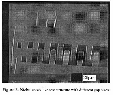
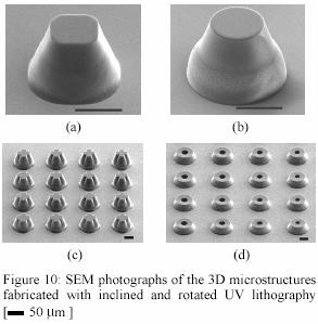
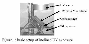
 Ji et al. Micro and Nano Systems Letters 2014, 2:6 LETTER Open Access Sidewall lithography of micron-sized features in high-aspect-ratio meso-scale channels using a three-dimensional assembled mask Chang-Hyeon
T in sec, I in W/cm 2, E in J/cm 2
 Exposures from Mask Aligner into Resist Mask aligner images created by shadowing from mask into resist Soft contact and Proximity good for 3 micron structures Vacuum Hard Contact: no shadow effects at
T in sec, I in W/cm 2, E in J/cm 2
 Exposures from Mask Aligner into Resist Mask aligner images created by shadowing from mask into resist Soft contact and Proximity good for 3 micron structures Vacuum Hard Contact: no shadow effects at
Diverse Lasers Support Key Microelectronic Packaging Tasks
 Diverse Lasers Support Key Microelectronic Packaging Tasks Written by D Muller, R Patzel, G Oulundsen, H Halou, E Rea 23 July 2018 To support more sophisticated and compact tablets, phones, watches and
Monolithically integrated InGaAs nanowires on 3D. structured silicon-on-insulator as a new platform for. full optical links
 Monolithically integrated InGaAs nanowires on 3D structured silicon-on-insulator as a new platform for full optical links Hyunseok Kim 1, Alan C. Farrell 1, Pradeep Senanayake 1, Wook-Jae Lee 1,* & Diana.
AZ 1512 RESIST PHOTOLITHOGRAPHY
 AZ 1512 RESIST PHOTOLITHOGRAPHY STANDARD OPERATIONAL PROCEDURE Faculty Supervisor: Prof. R. Bruce Darling Students: Katherine Lugo Danling Wang Department of Electrical Engineering Spring, 2009 TABLE OF
Synthesis of projection lithography for low k1 via interferometry
 Synthesis of projection lithography for low k1 via interferometry Frank Cropanese *, Anatoly Bourov, Yongfa Fan, Andrew Estroff, Lena Zavyalova, Bruce W. Smith Center for Nanolithography Research, Rochester
Design Rules for Silicon Photonics Prototyping
 Design Rules for licon Photonics Prototyping Version 1 (released February 2008) Introduction IME s Photonics Prototyping Service offers 248nm lithography based fabrication technology for passive licon-on-insulator
CMOS Digital Integrated Circuits Lec 2 Fabrication of MOSFETs
 CMOS Digital Integrated Circuits Lec 2 Fabrication of MOSFETs 1 CMOS Digital Integrated Circuits 3 rd Edition Categories of Materials Materials can be categorized into three main groups regarding their
Oxime Sulfonate Chemistry for Advanced Microlithography
 Journal of Photopolymer Science and Technology Volume 20, Number 5 (2007) 637-642 @TAPJ Oxime Sulfonate Chemistry for Advanced Microlithography Hitoshi Yamato, Toshikage Asakura, Yuichi Nishimae, Akira
T in sec, I in W/cm 2, E in J/cm 2
 Exposures from Mask Aligner into Resist Mask aligner images created by shadowing from mask into resist Soft contact and Proximity good for 3 micron structures Vacuum Hard Contact: no shadow effects at
Fabrication of suspended micro-structures using diffsuser lithography on negative photoresist
 Journal of Mechanical Science and Technology 22 (2008) 1765~1771 Journal of Mechanical Science and Technology www.springerlink.com/content/1738-494x DOI 10.1007/s12206-008-0601-8 Fabrication of suspended
Copyright 2000 by the Society of Photo-Optical Instrumentation Engineers.
 Copyright by the Society of Photo-Optical Instrumentation Engineers. This paper was published in the proceedings of Optical Microlithography XIII, SPIE Vol. 4, pp. 658-664. It is made available as an electronic
BI-LAYER DEEP UV RESIST SYSTEM. Mark A. Boehm 5th Year Microelectronic Engineering Student Rochester Institute of Technology ABSTRACT
 INTRODUCTION BI-LAYER DEEP UV RESIST SYSTEM Mark A. Boehm 5th Year Microelectronic Engineering Student Rochester Institute of Technology ABSTRACT A portable conformable mask (PCM) system employing KTIS2O
Polymers and Nanotechnology
 Polymers and Nanotechnology Grant Willson Department of Chemical Engineering Department of Chemistry The University of Texas Austin, Texas 78712 http://willson.cm.utexas.edu The Texas Tower Grad students
Surface Topography and Alignment Effects in UV-Modified Polyimide Films with Micron Size Patterns
 CHINESE JOURNAL OF PHYSICS VOL. 41, NO. 2 APRIL 2003 Surface Topography and Alignment Effects in UV-Modified Polyimide Films with Micron Size Patterns Ru-Pin Pan 1, Hua-Yu Chiu 1,Yea-FengLin 1,andJ.Y.Huang
Department of Astronomy, Graduate School of Science, the University of Tokyo, Hongo, Bunkyo-ku, Tokyo , Japan;
 Verification of the controllability of refractive index by subwavelength structure fabricated by photolithography: toward single-material mid- and far-infrared multilayer filters Hironobu Makitsubo* a,b,