KMPR 1010 Process for Glass Wafers
|
|
|
- Marianna Armstrong
- 5 years ago
- Views:
Transcription
1 KMPR 1010 Process for Glass Wafers KMPR 1010 Steps Protocol Step System Condition Note Plasma Cleaning PVA Tepla Ion 10 5 mins Run OmniCoat Receipt Dehydration Any Heat Plate 150 C, 5 mins HMDS Coating Brewer Spin Coater 250 rpm, 250rpm/s, 5 secs; 2000 rpm, 1000rpm/s,30 secs; 0 rpm, 1000rpm/s, 8 secs. KMPR 1010 Coating Brewer Spin Coater 500 rpm, 100rpm/s, 12 secs; 2000 rpm, 700rpm/s,35 secs; 3500 rpm, 1000rpm/s, 7 secs; 0 rpm, 1500rpm/s, 5 secs. Soft Bake Any Heat Plate 100 C, 7mins Exposure ABM Contact Aligner 410 MJ ( Steps exposure ) 10 Post Bake Any Heat Plate 100 C, 2mins Development AZ 300 MIF & H 2O 45 secs/30secs/15secs 12 N 2 Dry Use HMDS 20% spinon bottle
2 1. Place glass wafer in PVA Tepla Ion 10 and select the Omnicoat lift up recipe to ash the wafer. Edit the recipe and set plasma ignite to 5 minutes. This will clean the wafer and ensure better adhesion later in the process. 2. Dehydrate wafer on hot plate for 5 minutes at 150 C. After dehydration bake allow wafer to cool to room temperature. Note: If the contact aligner is not already on turn on the AB-M contact aligner to allow the bulb to warm up. 3. HMDS coating using the following recipe on the Brewer spin coater: I) Speed: 250 RPM, Ramp: 250 RPM/s, Time: 5 seconds II) Speed: 2000 RPM, Ramp: 700 RPM/s, Time: 35 seconds III) Speed: 0 RPM, Ramp: 1000 RPM/s, Time: 7 seconds 4. After HMDS spin, the wafer should look dry and clean. Remove the wafer from the chuck and rinse the bowl with acetone to remove the HMDS spill. 5. Cover the bowl of the Brewer Spin coater with Aluminum foil to avoid photoresist contact spill. 6. Place the wafer back on chuck and pour 15 to 20 ml of KMPR 1010 into center of wafer (this should cover more than 2/3 of the wafers surface) 7. Use the following recipe on the spin coater: I) Speed: 500 RPM, Ramp: 100 RPM/s, Time: 12 seconds II) Speed: 2000 RPM, Ramp: 700 RPM/s, Time: 35 seconds III) Speed: 3500 RPM, Ramp: 1000 RPM/s, Time: 7 seconds IV) Speed: 0 RPM, Ramp: 500 RPM/s, Time: 5 seconds 8. Being careful not to tilt the photoresist coated wafer, remove the wafer from the spinner and soft bake wafer on hot plate for 7 minutes at 100 C. After soft bake allow wafer to cool to room temperature before continuing process. 9. Insert i-line (365nm) filter into contact aligner. Open the nitrogen and vacuum valves to the right of the contact aligner. 10. Measure the intensity of contact aligner at each of the four corners of the stage as well as the center and take the average intensity. 11. Place wafer on the contact aligner substrate stage. Be sure to confirm that the substrate stage is below the mask stage. Place the lithography mask onto the mask stage and turn the mask vacuum and nitrogen flow on. While depressing the leveling chuck, raise the stage until relatively hard contact is made between the mask and wafer and turn the contact vacuum on. 12. Expose wafer so that the total intensity seen by the wafer is 410 mj. To calculate exposure time, take 410 mj and divide it by number of exposures and measured intensity. Exposures should be less than 15 seconds due to the fragile nature of the photoresist and should allow 30 seconds in between exposures to allow photoresist to cool. 13. Turn contact vacuum and nitrogen flow off. Lower the substrate stage, turn off the mask vacuum and remove the lithography mask. Now turn off the substrate vacuum. Remove the wafer and place on a hot plate to hard bake the wafer for 2 minutes at 100 C. After hard bake allow wafer to cool to room temperature. 14. Develop wafer pattern face up for 45 seconds in AZ300 MIF developer, transfer wafer to a water bath for 30 seconds, and then finally a second water bath for 15 seconds. 15. Dry with nitrogen gun. 16. Develop further as desired.


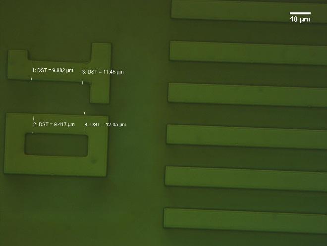
3 Result Expectation: for pattern dimensions larger than or equal to 10 micrometers in width and 11 microns in height, angles of approximately 95 degrees between photoresist and substrate can be achieved. Bright Field 100x Dark Field 100x


4 Under Exposed Images: Dark field bottom focus Bright field bottom focus Dark field top focus Bright field top focus Over Exposed Images: Dark field top focus Bright field top focus


5 Bright field top focus Bright field bottom focus Discussion: Exposure is the process of subjecting certain areas of a photoresist covered wafer to ultraviolet (UV) light. In the case of this study, glass wafers were spin coated with KMPR, a negative photoresist. Negative photoresists become cross-linked when exposed to UV light, and therefore are harder to dissolve with a developer. When developed, the areas on the wafer that have been exposed to UV light remain while the rest is washed away. Exposure dose largely affects the quality of the wafer because it is responsible for how much energy the photoresist absorbs from UV light. If the exposure dose is too low, the energy from the UV light will not reach the bottom of the photoresist coating and the pattern will start to "peel off" during development. If the exposure dose is too high, the energy from the UV light will spread to nearby parts of the wafer causing unexposed areas to be coated by a thin layer of photoresist even after development. An optimum exposure dose would produce approximately a 90-degree angle between the substrate and photoresist. This dosage would also produce a pattern without any photoresist in cave areas, an approximate photoresist height of 11 microns, and a width of 10 microns. The total optimum exposure dosage in this study was found to be 410 mj. Analysis Spin Rate o Standard deviations between the different wafers also appears to be consistent Exposure Time o Currently the best resolution(1µm) and aspect ratio(1:11) is being produced at a total intensity of 410 mj o Increasing exposure time slightly can achieve more undercut profile Reasoning: Microchem recommends 20-30% over exposure when attempting to produce an undercut profile with negative photoresist Pre-Procedure o Currently the main pre-procedure process is dehydration, a few processes have also implemented the plasma cleaning and HMDS coating which we believe could be beneficial to improving adhesion.
6 Development o We found that the methods of development could be adjusted upon different thickness and sizes of pattern. o The KMPR data sheet calls for an immediate spray rinse after development instead of soaking the wafer in a water bath. This spray rinse might be more effective at removing developer from between photoresist areas. However, it may also remove the pattern if the spray is not gently enough.
+ Preferred material for tool O Acceptable material for tool X Unacceptable material for tool
 Contact Aligners (HTG, ABM, EV620) GCA 5X g-line Stepper GCA i-line Steppers (GCA 10X, AS200) Shipley 1800 Series (1805, 1813, 1818, 1827) + + X AZ nlof 2000 O X + AZ4903 + + X OiR 620-7i X X + OiR 897-12i
AZ 1512 RESIST PHOTOLITHOGRAPHY
 AZ 1512 RESIST PHOTOLITHOGRAPHY STANDARD OPERATIONAL PROCEDURE Faculty Supervisor: Prof. R. Bruce Darling Students: Katherine Lugo Danling Wang Department of Electrical Engineering Spring, 2009 TABLE OF
Major Fabrication Steps in MOS Process Flow
 Major Fabrication Steps in MOS Process Flow UV light Mask oxygen Silicon dioxide photoresist exposed photoresist oxide Silicon substrate Oxidation (Field oxide) Photoresist Coating Mask-Wafer Alignment
Semiconductor Manufacturing Technology. Semiconductor Manufacturing Technology. Photolithography: Resist Development and Advanced Lithography
 Semiconductor Manufacturing Technology Michael Quirk & Julian Serda October 2001 by Prentice Hall Chapter 15 Photolithography: Resist Development and Advanced Lithography Eight Basic Steps of Photolithography
Part 5-1: Lithography
 Part 5-1: Lithography Yao-Joe Yang 1 Pattern Transfer (Patterning) Types of lithography systems: Optical X-ray electron beam writer (non-traditional, no masks) Two-dimensional pattern transfer: limited
SU-8 Post Development Bake (Hard Bake) Study
 Study") University of Pennsylvania ScholarlyCommons Protocols and Reports Browse by Type 10-16-2017 Ram Surya Gona University of Pennsylvania, ramgona@seas.upenn.edu Eric D. Johnston Singh Center for Nanotechnology,
University of Pennsylvania ScholarlyCommons Protocols and Reports Browse by Type 10-16-2017 Ram Surya Gona University of Pennsylvania, ramgona@seas.upenn.edu Eric D. Johnston Singh Center for Nanotechnology,
Device Fabrication: Photolithography
 Device Fabrication: Photolithography 1 Objectives List the four components of the photoresist Describe the difference between +PR and PR Describe a photolithography process sequence List four alignment
FINDINGS. REU Student: Philip Garcia Graduate Student Mentor: Anabil Chaudhuri Faculty Mentor: Steven R. J. Brueck. Figure 1
 FINDINGS REU Student: Philip Garcia Graduate Student Mentor: Anabil Chaudhuri Faculty Mentor: Steven R. J. Brueck A. Results At the Center for High Tech Materials at the University of New Mexico, my work
Dr. Dirk Meyners Prof. Wagner. Wagner / Meyners Micro / Nanosystems Technology
 Micro/Nanosystems Technology Dr. Dirk Meyners Prof. Wagner 1 Outline - Lithography Overview - UV-Lithography - Resolution Enhancement Techniques - Electron Beam Lithography - Patterning with Focused Ion
Etching Small Samples and the Effects of Using a Carrier Wafer STS ICP-RIE
 Etching Small Samples and the Effects of Using a Carrier Wafer STS ICP-RIE This note is a brief description of the effects of bonding pieces to a carrier wafer during the etch process on the STS ICP-RIE.
Prototype PCBs implementatio n session
 Prototype PCBs implementatio n session By: Dr. Ahmed ElShafee ١ Dr. Ahmed ElShafee, ACU : Spring 2018, EEP04 Practical Applications in Electrical ٢ photo resistive PCB ٣ Step 1 : print PCB on translucent
Lecture 7. Lithography and Pattern Transfer. Reading: Chapter 7
 Lecture 7 Lithography and Pattern Transfer Reading: Chapter 7 Used for Pattern transfer into oxides, metals, semiconductors. 3 types of Photoresists (PR): Lithography and Photoresists 1.) Positive: PR
Lecture (03.02) PCB fabrication using. and toner thermal transferee By: Dr. Ahmed ElShafee
 PCB fabrication using. and toner thermal transferee By: Dr. Ahmed ElShafee") Lecture (03.02) PCB fabrication using photo resistive PCB and toner thermal transferee By: Dr. Ahmed ElShafee ١ Dr. Ahmed ElShafee, ACU : Spring 2017, Practical App EE IV photo resistive PCB ٢ Step 1 :
Lecture (03.02) PCB fabrication using photo resistive PCB and toner thermal transferee By: Dr. Ahmed ElShafee ١ Dr. Ahmed ElShafee, ACU : Spring 2017, Practical App EE IV photo resistive PCB ٢ Step 1 :
Photolithography Technology and Application
 Photolithography Technology and Application Jeff Tsai Director, Graduate Institute of Electro-Optical Engineering Tatung University Art or Science? Lind width = 100 to 5 micron meter!! Resolution = ~ 3
UFNF YES Image Reversal & HMDS Oven Revision 6.0 1/22/2014 Page 1 of 5. YES Image Reversal and HMDS Oven SOP
 1/22/2014 Page 1 of 5 YES Image Reversal and HMDS Oven SOP Table of Contents 1.0 Safety 2.0 Quality Control and Calibrations 3.0 Processes Description 4.0 Process Information for Lift Off 5.0 Operation
EG2605 Undergraduate Research Opportunities Program. Large Scale Nano Fabrication via Proton Lithography Using Metallic Stencils
 EG2605 Undergraduate Research Opportunities Program Large Scale Nano Fabrication via Proton Lithography Using Metallic Stencils Tan Chuan Fu 1, Jeroen Anton van Kan 2, Pattabiraman Santhana Raman 2, Yao
i- Line Photoresist Development: Replacement Evaluation of OiR
 i- Line Photoresist Development: Replacement Evaluation of OiR 906-12 Nishtha Bhatia High School Intern 31 July 2014 The Marvell Nanofabrication Laboratory s current i-line photoresist, OiR 897-10i, has
William Reiniach 5th Year Microelectronic Engineering Student Rochester Institute of Technology
 DEVELOPMENT OF A PHOTOSENSITIVE POLYIMIDE PROCESS William Reiniach 5th Year Microelectronic Engineering Student Rochester Institute of Technology 1~BS TRACT A six step lithographic process has been developed
Photolithography I ( Part 1 )
") 1 Photolithography I ( Part 1 ) Chapter 13 : Semiconductor Manufacturing Technology by M. Quirk & J. Serda Bjørn-Ove Fimland, Department of Electronics and Telecommunication, Norwegian University of Science
1 Photolithography I ( Part 1 ) Chapter 13 : Semiconductor Manufacturing Technology by M. Quirk & J. Serda Bjørn-Ove Fimland, Department of Electronics and Telecommunication, Norwegian University of Science
Heidelberg µpg 101 Laser Writer
 Heidelberg µpg 101 Laser Writer Standard Operating Procedure Revision: 3.0 Last Updated: Aug.1/2012, Revised by Nathanael Sieb Overview This document will provide a detailed operation procedure of the
OPTICAL LITHOGRAPHY USING LASERWRITER LW405
 OPTICAL LITHOGRAPHY USING LASERWRITER LW405 Tool identifier: LaserWriter LW405 SYSTEM OWNER/OPERATOR AKHIL KUMAR ARATHY MENON CONTACT DETAILS akhilatnik@ee.iitb.ac.in arathymenoniit@gmail.com arathy_menon@iitb.ac.in
(ksaligner & quintel resolution)
") Process [4.10] (ksaligner & quintel resolution) 1.0 Process Summary 1.1 Since Karl Suss ksaligner is heavily used and Quintel aligner is not, nanolab decided to compare the 2 micron line resolution from
Process [4.10] (ksaligner & quintel resolution) 1.0 Process Summary 1.1 Since Karl Suss ksaligner is heavily used and Quintel aligner is not, nanolab decided to compare the 2 micron line resolution from
BI-LAYER DEEP UV RESIST SYSTEM. Mark A. Boehm 5th Year Microelectronic Engineering Student Rochester Institute of Technology ABSTRACT
 INTRODUCTION BI-LAYER DEEP UV RESIST SYSTEM Mark A. Boehm 5th Year Microelectronic Engineering Student Rochester Institute of Technology ABSTRACT A portable conformable mask (PCM) system employing KTIS2O
Contrast Enhancement Materials CEM 365iS
 INTRODUCTION In 1989 Shin-Etsu Chemical acquired MicroSi, Inc. and the Contrast Enhancement Material (CEM) technology business from General Electric including a series of patents and technologies*. A concentrated
T in sec, I in W/cm 2, E in J/cm 2
 Exposures from Mask Aligner into Resist Mask aligner images created by shadowing from mask into resist Soft contact and Proximity good for 3 micron structures Vacuum Hard Contact: no shadow effects at
Lecture 13 Basic Photolithography
 Lecture 13 Basic Photolithography Chapter 12 Wolf and Tauber 1/64 Announcements Homework: Homework 3 is due today, please hand them in at the front. Will be returned one week from Thursday (16 th Nov).
Contrast Enhancement Materials CEM 365HR
 INTRODUCTION In 1989 Shin-Etsu Chemical acquired MicroSi, Inc. including their Contrast Enhancement Material (CEM) technology business*. A concentrated effort in the technology advancement of a CEM led
Semiconductor Technology
 Semiconductor Technology from A to Z + - x 1 0 x Photolithographie www.halbleiter.org Contents Contents List of Figures III 1 Photolithographie 1 1.1 Exposure and resist coating..........................
EE 143 Microfabrication Technology Fall 2014
 EE 143 Microfabrication Technology Fall 2014 Prof. Clark T.-C. Nguyen Dept. of Electrical Engineering & Computer Sciences University of California at Berkeley Berkeley, CA 94720 EE 143: Microfabrication
Outline. 1 Introduction. 2 Basic IC fabrication processes. 3 Fabrication techniques for MEMS. 4 Applications. 5 Mechanics issues on MEMS MDL NTHU
 Outline 1 Introduction 2 Basic IC fabrication processes 3 Fabrication techniques for MEMS 4 Applications 5 Mechanics issues on MEMS 2.2 Lithography Reading: Runyan Chap. 5, or 莊達人 Chap. 7, or Wolf and
Microlens formation using heavily dyed photoresist in a single step
 Microlens formation using heavily dyed photoresist in a single step Chris Cox, Curtis Planje, Nick Brakensiek, Zhimin Zhu, Jonathan Mayo Brewer Science, Inc., 2401 Brewer Drive, Rolla, MO 65401, USA ABSTRACT
MeRck. AZ nlof technical datasheet. Negative Tone Photoresist for Single Layer Lift-Off APPLICATION TYPICAL PROCESS. SPIN CURVE (150MM Silicon)
") MeRck technical datasheet AZ nlof 5510 Negative Tone Photoresist for Single Layer Lift-Off APPLICATION AZ nlof 5510 i-line photoresist is engineered to simplify the historically complex image reversal
MeRck technical datasheet AZ nlof 5510 Negative Tone Photoresist for Single Layer Lift-Off APPLICATION AZ nlof 5510 i-line photoresist is engineered to simplify the historically complex image reversal
MeRck. nlof 2000 Series. technical datasheet. Negative Tone Photoresists for Single Layer Lift-Off APPLICATION TYPICAL PROCESS
 MeRck technical datasheet AZ Negative Tone Photoresists for Single Layer Lift-Off APPLICATION AZ i-line photoresists are engineered to simplify the historically complex image reversal and multilayer lift-off
OPTOFLUIDIC ULTRAHIGH-THROUGHPUT DETECTION OF FLUORESCENT DROPS. Electronic Supplementary Information
 Electronic Supplementary Material (ESI) for Lab on a Chip. This journal is The Royal Society of Chemistry 2015 OPTOFLUIDIC ULTRAHIGH-THROUGHPUT DETECTION OF FLUORESCENT DROPS Minkyu Kim 1, Ming Pan 2,
PHGN/CHEN/MLGN 435/535: Interdisciplinary Silicon Processing Laboratory. Simple Si solar Cell!
 Where were we? Simple Si solar Cell! Two Levels of Masks - photoresist, alignment Etch and oxidation to isolate thermal oxide, deposited oxide, wet etching, dry etching, isolation schemes Doping - diffusion/ion
Module 11: Photolithography. Lecture11: Photolithography - I
 Module 11: Photolithography Lecture11: Photolithography - I 1 11.0 Photolithography Fundamentals We will all agree that incredible progress is happening in the filed of electronics and computers. For example,
Lesson Plan Title Primary Subject Area Grade Level Overview Approximate Duration MA Frameworks Interdisciplinary Connections Lesson Objectives
 Lesson Plan Title Screenprinting/photolithography and understanding MEMS production and their application Primary Subject Area Chemistry Grade Level High School (10) Overview Students will learn about
Soft Electronics Enabled Ergonomic Human-Computer Interaction for Swallowing Training
 Supplementary Information Soft Electronics Enabled Ergonomic Human-Computer Interaction for Swallowing Training Yongkuk Lee 1,+, Benjamin Nicholls 2,+, Dong Sup Lee 1, Yanfei Chen 3, Youngjae Chun 3,4,
T in sec, I in W/cm 2, E in J/cm 2
 Exposures from Mask Aligner into Resist Mask aligner images created by shadowing from mask into resist Soft contact and Proximity good for 3 micron structures Vacuum Hard Contact: no shadow effects at
THE USE OF A CONTRAST ENHANCEMENT LAYER TO EXTEND THE PRACTICAL RESOLUTION LIMITS OF OPTICAL LITHOGRAPHIC SYSTEMS
 THE USE OF A CONTRAST ENHANCEMENT LAYER TO EXTEND THE PRACTICAL RESOLUTION LIMITS OF OPTICAL LITHOGRAPHIC SYSTEMS Daniel R. Sutton 5th Year Microelectronic Engineering Student Rochester Institute of Technology
MICROSTRUCTURING OF METALLIC LAYERS FOR SENSOR APPLICATIONS
 MICROSTRUCTURING OF METALLIC LAYERS FOR SENSOR APPLICATIONS Vladimír KOLAŘÍK, Stanislav KRÁTKÝ, Michal URBÁNEK, Milan MATĚJKA, Jana CHLUMSKÁ, Miroslav HORÁČEK, Institute of Scientific Instruments of the
Chapter 3 Fabrication
 Chapter 3 Fabrication The total structure of MO pick-up contains four parts: 1. A sub-micro aperture underneath the SIL The sub-micro aperture is used to limit the final spot size from 300nm to 600nm for
MICROBUMP CREATION SYSTEM FOR ADVANCED PACKAGING APPLICATIONS
 MICROBUMP CREATION SYSTEM FOR ADVANCED PACKAGING APPLICATIONS Andrew Ahr, EKC Technology, & Chester E. Balut, DuPont Electronic Technologies Alan Huffman, RTI International Abstract Today, the electronics
Chapter 6. Photolithography
 Chapter 6 Photolithography 2006/4/10 1 Objectives List the four components of the photoresist Describe the difference between +PR and PR Describe a photolithography process sequence List four alignment
(2) The resist now would behave like an exposed positive resist. soluble
 The resist now would behave like an exposed positive resist. soluble") Processing image reversal s... symptoms, diagnosis, and trouble-shooting revised 2003-09-25 General information about image reversal s Detailed processing guidelines are given in the individual technical
Processing image reversal s... symptoms, diagnosis, and trouble-shooting revised 2003-09-25 General information about image reversal s Detailed processing guidelines are given in the individual technical
EXPERIMENT # 3: Oxidation and Etching Tuesday 2/3/98 and 2/5/98 Thursday 2/10/98 and 2/12/98
 EXPERIMENT # 3: Oxidation and Etching Tuesday 2/3/98 and 2/5/98 Thursday 2/10/98 and 2/12/98 Experiment # 3: Oxidation of silicon - Oxide etching and Resist stripping Measurement of oxide thickness using
Photolithography II ( Part 2 )
") 1 Photolithography II ( Part 2 ) Chapter 14 : Semiconductor Manufacturing Technology by M. Quirk & J. Serda Saroj Kumar Patra, Department of Electronics and Telecommunication, Norwegian University of Science
1 Photolithography II ( Part 2 ) Chapter 14 : Semiconductor Manufacturing Technology by M. Quirk & J. Serda Saroj Kumar Patra, Department of Electronics and Telecommunication, Norwegian University of Science
College of Engineering Department of Electrical Engineering and Computer Sciences University of California, Berkeley
 College of Engineering Department of Electrical Engineering and Below are your weekly quizzes. You should print out a copy of the quiz and complete it before your lab section. Bring in the completed quiz
Standard Operating Manual
 Standard Operating Manual Buehler EcoMet TM 300 Polisher Version 1.0 Page 1 of 19 Contents 1. Picture and Location 2. Process Capabilities 2.1 Cleanliness Standard 2.2 Possible Polishing Materials 2.3
Micro/Nanolithography
 Dale E. Ewbank dale.ewbank@rit.edu unl081413_microe.ppt 2013 Dale E. Ewbank page 1 OUTLINE Masks Optical Lithography Photoresist Sensitivity Processing Exposure Tools Advanced Processes page 2 MICROLITHOGRAPHY
Fabrication Methodology of microlenses for stereoscopic imagers using standard CMOS process. R. P. Rocha, J. P. Carmo, and J. H.
 Fabrication Methodology of microlenses for stereoscopic imagers using standard CMOS process R. P. Rocha, J. P. Carmo, and J. H. Correia Department of Industrial Electronics, University of Minho, Campus
EXPERIMENT # 3: Oxidation and Etching Week of 1/31/05 and 2/7/05
 EXPERIMENT # 3: Oxidation and Etching Week of 1/31/05 and 2/7/05 Experiment # 3: Oxidation of silicon - Oxide etching and Resist stripping Measurement of oxide thickness using different methods The purpose
Chapter 6 Photolithography
 Chapter 6 Photolithography Hong Xiao, Ph. D. hxiao89@hotmail.com www2.austin.cc.tx.us/hongxiao/book.htm Hong Xiao, Ph. D. www2.austin.cc.tx.us/hongxiao/book.htm 1 Objectives List the four components of
Low-power carbon nanotube-based integrated circuits that can be transferred to biological surfaces
 SUPPLEMENTARY INFORMATION Articles https://doi.org/10.1038/s41928-018-0056-6 In the format provided by the authors and unedited. Low-power carbon nanotube-based integrated circuits that can be transferred
Technology for the MEMS processing and testing environment. SUSS MicroTec AG Dr. Hans-Georg Kapitza
 Technology for the MEMS processing and testing environment SUSS MicroTec AG Dr. Hans-Georg Kapitza 1 SUSS MicroTec Industrial Group Founded 1949 as Karl Süss KG GmbH&Co. in Garching/ Munich San Jose Waterbury
Clay Modeling Film. Features of Clay Modeling Film. Use Clay Modeling Film
 Clay Modeling Film The series of Clay Modeling Film, originally developed by TOOLS INTERNATIONAL Corp, is mainly used for interior/exterior shape confirmation, checking highlights and qualification studies
Lithography. 3 rd. lecture: introduction. Prof. Yosi Shacham-Diamand. Fall 2004
 Lithography 3 rd lecture: introduction Prof. Yosi Shacham-Diamand Fall 2004 1 List of content Fundamental principles Characteristics parameters Exposure systems 2 Fundamental principles Aerial Image Exposure
Electrical Impedance Spectroscopy for Microtissue Spheroid Analysis in Hanging-Drop Networks
 Electrical Impedance Spectroscopy for Microtissue Spheroid Analysis in Hanging-Drop Networks Yannick R. F. Schmid, Sebastian C. Bürgel, Patrick M. Misun, Andreas Hierlemann, and Olivier Frey* ETH Zurich,
Obducat NIL 6. Nanoimprinting with NRF s NIL 6
 Obducat NIL 6 Substrates: pieces to 6 inch, hard or soft Thermal cure with PMMA, MR I 7010 etc Alignment to about 3 microns Temperature to 300 HC Pressure 15 to 80 bars Resolution < 50 nm possible Up to
E3 UV-30 Resist Film Instructions
 E3 UV-30 Resist Film Instructions For more information or to view instructions in color, visit www.sherrihaab.com Sherri Haab Designs 2016 Supplies needed: Metal plate to etch (copper, brass or silver)
TEM SAMPLE-PREPARATION PROCEDURES FOR THIN-FILM MATERIALS
 TEM SAMPLE-PREPARATION PROCEDURES FOR THIN-FILM MATERIALS Initial Set-Up: Heat up a hot plate to around 150-200 C Plan view Mounting/Grinding/Dimpling/Polishing: 1) Cleave a square-ish piece of sample.
Supplement: Fabrication protocol
 Supplement: Fabrication protocol The present series of protocols details how to fabricate both silica microsphere and microtoroid resonant cavities. While silica microsphere resonant cavities are wellestablished,
DOE Project: Resist Characterization
 DOE Project: Resist Characterization GOAL To achieve high resolution and adequate throughput, a photoresist must possess relatively high contrast and sensitivity to exposing radiation. The objective of
MURAKAMI THICK FILM APPLICATION GUIDE PRESENTED BY: BOB WELLEN
 MURAKAMI THICK FILM APPLICATION GUIDE PRESENTED BY: BOB WELLEN Why Use Murakami MS-Thick Film? Murakami has been producing MS-Thick Film for 13 years. Our experience in this particular area of screen printing
MICROLITHOGRAPHY 2004
 MICROLITHOGRAPHY 2004 From Computer Aided Design (CAD) to Patterned Substrate At the CNF, a number of different options exist for producing a patterned substrate, but deciding which option is best for
Integrated Focusing Photoresist Microlenses on AlGaAs Top-Emitting VCSELs
 Integrated Focusing Photoresist Microlenses on AlGaAs Top-Emitting VCSELs Andrea Kroner We present 85 nm wavelength top-emitting vertical-cavity surface-emitting lasers (VCSELs) with integrated photoresist
Instruction Guide Basic Instructions 2... Appliying the Dye 3... Creating an Image 4... Exposing Your Print 5... Washing
 Instruction Guide 2... Basic Instructions 2... Appliying the Dye 3... Creating an Image 4... Exposing Your Print 5... Washing SolarFast dyes are used to create photograms, continuous tone photographs,
MOLD INSTRUCTION MANUAL
 ProFiller RDT MOLD INSTRUCTION MANUAL Disclaimer: For use in prescription pharmacy compounding only, in accordance with applicable law. MEDISCA makes no warranty or representation regarding the use of
MicroPG 101 Pattern Generator Standard Operating Procedure Draft v.0.2
 Tool owner: Roman Akhmechet, romana@princeton.edu, x 8-0468 Backup: David Barth, dbarth@princeton.edu MicroPG 101 Pattern Generator Standard Operating Procedure Draft v.0.2 QUICK GUIDE PROCEDURE OVERVIEW
All-Glass Gray Scale PhotoMasks Enable New Technologies. Che-Kuang (Chuck) Wu Canyon Materials, Inc.
 Wu Canyon Materials, Inc.") All-Glass Gray Scale PhotoMasks Enable New Technologies Che-Kuang (Chuck) Wu Canyon Materials, Inc. 1 Overview All-Glass Gray Scale Photomask technologies include: HEBS-glasses and LDW-glasses HEBS-glass
All-Glass Gray Scale PhotoMasks Enable New Technologies Che-Kuang (Chuck) Wu Canyon Materials, Inc. 1 Overview All-Glass Gray Scale Photomask technologies include: HEBS-glasses and LDW-glasses HEBS-glass
EE-527: MicroFabrication
 EE-57: MicroFabrication Exposure and Imaging Photons white light Hg arc lamp filtered Hg arc lamp excimer laser x-rays from synchrotron Electrons Ions Exposure Sources focused electron beam direct write
Conformal Electronics Wrapped Around Daily-life Objects. Using Original Method: Water Transfer Printing.
 Supporting Information Conformal Electronics Wrapped Around Daily-life Objects Using Original Method: Water Transfer Printing. Brice Le Borgne, Olivier De Sagazan, Samuel Crand, Emmanuel Jacques, Maxime
Nanoscale Fabrication & Characterization Facility. Raith e-line EBL Users Guide (updated:aug 2 nd, 2017)
") Nanoscale Fabrication & Characterization Facility Raith e-line EBL Users Guide (updated:aug 2 nd, 2017) Overview: The Raith e-line EBL system is designed to write features with critical dimensions as small
Nanoscale Fabrication & Characterization Facility Raith e-line EBL Users Guide (updated:aug 2 nd, 2017) Overview: The Raith e-line EBL system is designed to write features with critical dimensions as small
Fabrication of suspended micro-structures using diffsuser lithography on negative photoresist
 Journal of Mechanical Science and Technology 22 (2008) 1765~1771 Journal of Mechanical Science and Technology www.springerlink.com/content/1738-494x DOI 10.1007/s12206-008-0601-8 Fabrication of suspended
Module 11: Photolithography. Lecture 14: Photolithography 4 (Continued)
") Module 11: Photolithography Lecture 14: Photolithography 4 (Continued) 1 In the previous lecture, we have discussed the utility of the three printing modes, and their relative advantages and disadvantages.
Module 11: Photolithography Lecture 14: Photolithography 4 (Continued) 1 In the previous lecture, we have discussed the utility of the three printing modes, and their relative advantages and disadvantages.
FORMULARY P.O. Box 950 Condon MT FAX
 Catalog Number 07-0080 PHOTOGRAPHERS' FORMULARY P.O. Box 950 Condon MT 59826 800-922-5255 FAX 406-754-2896 Van Dyke Brown Printing Kit Contains chemicals to make approximately 100 4 x 5 prints As the name
SUSS Mask Aligner. Purpose: To expose photoresist on a wafer using a photomask
 SUSS Mask Aligner Purpose: To expose photoresist on a wafer using a photomask Overview This SOP will go over how to use the machine for basic exposures. This will include commonly used controls and frequently
University of Minnesota Nano Fabrication Center Standard Operating Procedure Equipment Name:
 Equipment Name: Coral Name: Nanoimprinter Revision Number: 1.1 Model: NX-B200 Revisionist: M. Fisher Location: Bay 4 Date: 2/12/2010 1 Description Nanonex NX-B200 nanoimprinter is another method of transfer
Applications of Maskless Lithography for the Production of Large Area Substrates Using the SF-100 ELITE. Jay Sasserath, PhD
 Applications of Maskless Lithography for the Production of Large Area Substrates Using the SF-100 ELITE Executive Summary Jay Sasserath, PhD Intelligent Micro Patterning LLC St. Petersburg, Florida Processing
MICRO AND NANOPROCESSING TECHNOLOGIES
 MICRO AND NANOPROCESSING TECHNOLOGIES LECTURE 4 Optical lithography Concepts and processes Lithography systems Fundamental limitations and other issues Photoresists Photolithography process Process parameter
Photoresist Absorbance and Bleaching Laboratory
 MCEE 505 Lithography Materials and Processes Page 1 of 5 Photoresist Absorbance and Bleaching Laboratory Microelectronic Engineering Rochester Institute of Technology 1. OBJECTIVE The objective of this
MOLD INSTRUCTION MANUAL
 Medi-RDT MOLD INSTRUCTION MANUAL Disclaimer: For use in prescription pharmacy compounding only, in accordance with applicable law. MEDISCA makes no warranty or representation regarding the use of this
Positive-Tone Photosensitive Polyimide Coatings for Lens Layer in image sensors. Introduction of the characteristic of CS-series
 Positive-Tone Photosensitive Polyimide Coatings for Lens Layer in image sensors Photoneece CS-series Introduction of the characteristic of CS-series Toray Industries, Inc. 1 1 CS-7500 basic properties
Mary L. Long * KTI Chemicals, Inc N. Camino Arco, Tucson, AZ Abstract. Introduction
 IMAGE REVERSAL TECHNIQUES WITH STANDARD POSITIVE PHOTORESIST Mary L. Long * KTI Chemicals, Inc. 4040 N. Camino Arco, Tucson, AZ. 85718 Jeff Newman Electrical and Computer Engineering, College of Engineering
POLYMER MICROSTRUCTURE WITH TILTED MICROPILLAR ARRAY AND METHOD OF FABRICATING THE SAME
 POLYMER MICROSTRUCTURE WITH TILTED MICROPILLAR ARRAY AND METHOD OF FABRICATING THE SAME Field of the Invention The present invention relates to a polymer microstructure. In particular, the present invention
TECHNICAL INFORMATION Küsnacht, February 2004 (rev. 1/09) THICKFILM STENCILS FOTECOAT 1845 SOLO
 THICKFILM STENCILS FOTECOAT 1845 SOLO") Fotec AG Eigenheimstr. 22 CH-8700 Küsnacht P.O.Box 1123 Switzerland Phone: +41 44 913 30 00 Fax: +41 44 910 45 25 e-mail: info@fotec.ch www.fotec.ch TECHNICAL INFORMATION Küsnacht, February 2004 (rev.
Fotec AG Eigenheimstr. 22 CH-8700 Küsnacht P.O.Box 1123 Switzerland Phone: +41 44 913 30 00 Fax: +41 44 910 45 25 e-mail: info@fotec.ch www.fotec.ch TECHNICAL INFORMATION Küsnacht, February 2004 (rev.
Supplementary Materials for
 www.sciencemag.org/cgi/content/full/science.1234855/dc1 Supplementary Materials for Taxel-Addressable Matrix of Vertical-Nanowire Piezotronic Transistors for Active/Adaptive Tactile Imaging Wenzhuo Wu,
SUSS MA/BA Gen4 Series COMPACT MASK ALIGNER PLATFORM FOR RESEARCH AND LOW-VOLUME PRODUCTION
 SEMI-AUTOMATED MASK ALIGNER SUSS MA/BA Gen4 Series COMPACT MASK ALIGNER PLATFORM FOR RESEARCH AND LOW-VOLUME PRODUCTION SEMI-AUTOMATED MASK ALIGNER SUSS MA/BA Gen4 Series SMART FULL-FIELD EXPOSURE TOOL
CMOS Digital Integrated Circuits Lec 2 Fabrication of MOSFETs
 CMOS Digital Integrated Circuits Lec 2 Fabrication of MOSFETs 1 CMOS Digital Integrated Circuits 3 rd Edition Categories of Materials Materials can be categorized into three main groups regarding their
NOTE: This product can be used externally if UV Guard is added (BY REQUEST ONLY).
.") Product Description PHOENIX PAINTS MAXICOAT 100 is a 2 Pack Water-Dispersed Top Coat which not only exhibits the physical and chemical strengths of epoxy, but also the safety and convenience of water as
Product Description PHOENIX PAINTS MAXICOAT 100 is a 2 Pack Water-Dispersed Top Coat which not only exhibits the physical and chemical strengths of epoxy, but also the safety and convenience of water as
Ultra-violet lithography of thick photoresist for the applications in BioMEMS and micro optics
 Louisiana State University LSU Digital Commons LSU Doctoral Dissertations Graduate School 2006 Ultra-violet lithography of thick photoresist for the applications in BioMEMS and micro optics Ren Yang Louisiana
SCREEN PRINTING TUTORIAL
 SCREEN PRINTING TUTORIAL print on any flat surface Make custom packaging for your project Experiment with biodegradable inks ONLINE BOOKING & REPOSITORY Film Positive In preparing your motif for print,
Polymer Plate Development Procedures. (800) or (802) (800)
 or (802) (800)") Polymer Plate ment Procedures (800) 272-7764 or (802) 362-0844 www.epsvt.com 1 www.epsvt.com (800) 272-7764 Introduction Understanding Plate Making Polymer plates consist of a photosensitive material which
Polymer Plate ment Procedures (800) 272-7764 or (802) 362-0844 www.epsvt.com 1 www.epsvt.com (800) 272-7764 Introduction Understanding Plate Making Polymer plates consist of a photosensitive material which
Key Photolithographic Outputs
 Exposure latitude Depth of Focus Exposure latitude Vs DOF plot Linearity and MEEF Isolated-Dense Bias NILS Contrast Swing Curve Reflectivity Curve 1 Exposure latitude:the range of exposure energies (usually
MLA 150 (DLA) Presentation and examples. Théophane Besson, , Heidelberg Instruments GmbH 1
 Presentation and examples. Théophane Besson, , Heidelberg Instruments GmbH 1") MLA 150 (DLA) Presentation and examples Théophane Besson, 17.03.2015, Heidelberg Instruments GmbH 1 Presentation of the tool The MLA 150 (named DLA in the past) is a new generation Maskless Aligner developed
MLA 150 (DLA) Presentation and examples Théophane Besson, 17.03.2015, Heidelberg Instruments GmbH 1 Presentation of the tool The MLA 150 (named DLA in the past) is a new generation Maskless Aligner developed
Standard Operating Manual
 Standard Operating Manual NanoFactor NVG-200A Silicon Grinder Version 1.1 Page 1 of 18 Contents 1. Picture and Location 2. Process Capabilities 2.1 Cleanliness Standard 2.2 Possible Grinding Materials
Microlithography. Dale E. Ewbank ul ppt. Microlithography Dale E. Ewbank page 1
 Dale E. Ewbank dale.ewbank@rit.edu ul012014.ppt 2014 Dale E. Ewbank page 1 OUTLINE Masks Optical Lithography Photoresist Sensitivity Processing Exposure Tools Advanced Processes page 2 MICROLITHOGRAPHY
Capillary Film Troubleshooting. Pinholes. Stencil underexposed
 Capillary Film Troubleshooting Pinholes Dust on exposure glass, film positive or capillary film Capillary film too thin for mesh count Fabric too dry during film application Emulsion incompatible with
Structural, optical, and electrical properties of phasecontrolled cesium lead iodide nanowires
 Electronic Supplementary Material Structural, optical, and electrical properties of phasecontrolled cesium lead iodide nanowires Minliang Lai 1, Qiao Kong 1, Connor G. Bischak 1, Yi Yu 1,2, Letian Dou
T in sec, I in W/cm 2, E in J/cm 2
 Exposures from Mask Aligner into Resist Mask aligner images created by shadowing from mask into resist Soft contact and Proximity good for 3 micron structures Vacuum Hard Contact: no shadow effects at