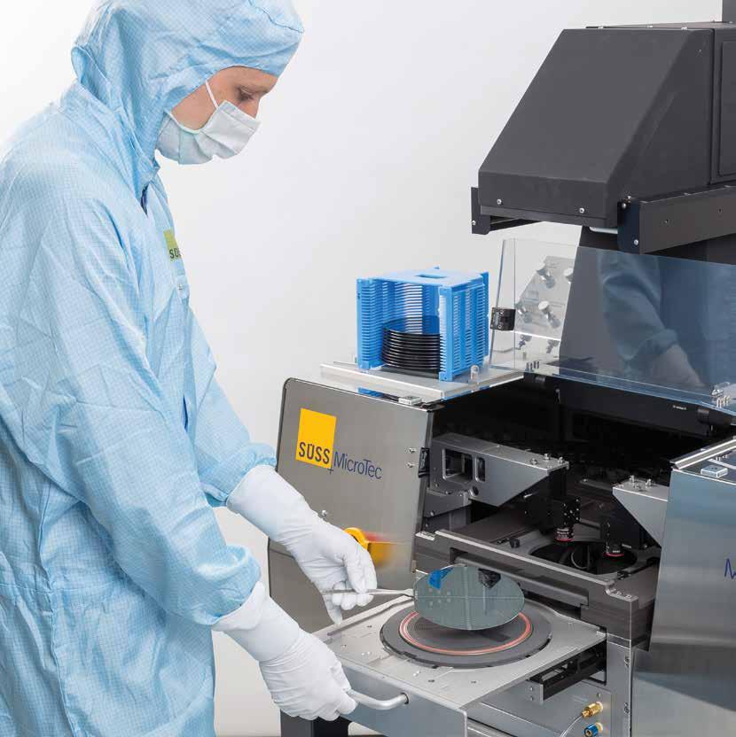
SUSS MA/BA Gen4 Series COMPACT MASK ALIGNER PLATFORM FOR RESEARCH AND LOW-VOLUME PRODUCTION
|
|
|
- Aleesha Marjorie Wade
- 5 years ago
- Views:
Transcription

1 SEMI-AUTOMATED MASK ALIGNER SUSS MA/BA Gen4 Series COMPACT MASK ALIGNER PLATFORM FOR RESEARCH AND LOW-VOLUME PRODUCTION


2 SEMI-AUTOMATED MASK ALIGNER SUSS MA/BA Gen4 Series SMART FULL-FIELD EXPOSURE TOOL The MA/BA Gen4 series represents the latest generation of SUSS MicroTec s semi-automated Mask and Bond Aligner introducing a new platform system. There are two platform types that differ in configuration. The MA/BA Gen4 is suited for standard processes and the MA/BA Gen4 Pro Series is designed for advanced and high-end processes. The MA/BA Gen4 series is the entry-level model, available as MA/BA6 Gen4 and MA/BA8 Gen4. With its enhanced ergonomic and user-friendly design, cost efficiency and reduced footprint, it is the perfect tool for use in research and lowvolume production. SUSS MicroTec s MA/BA Gen4 series is setting a new benchmark in full-field lithography for academia, MEMS & NEMS, 3D integration and compound semiconductor markets. It is also prepared to handle processes like bond alignment, fusion bonding and SMILE imprint. Processes developed on the MA/BA Gen4 series can be quickly transferred onto SUSS MicroTec s automated mask aligner platforms for high-volume production. OPTIONS + High precision wafer-to-wafer alignment + Imprint lithography for full-surface patterning (SMILE) + Fusion bonding + Bond Alignment + LAB Simulation Software + Source-Mask Optimization MA/BA Gen4 Series HIGHLIGHTS + High level of automation + Superior top-side, bottom-side, and infrared alignment technologies + Handles multiple substrate shapes and sizes + Reliable processing of fragile, warped or uneven surfaces + Enhanced ergonomic design 2


3 APPLICATIONS IN RESEARCH AND PRODUCTION MEMS The highly uniform, light-shaping exposure optics of the MA/BA Gen4 series is ideal for processing thick-resist MEMS applications. Features like bottom-side or infrared alignment (transmission or reflective illumination), bond alignment and the capability to process any type of substrate make the platform an enabling lithography tool for development and low-volume production of MEMS devices. ACADEMIA The MA/BA Gen4 series is versatile and easy to use, which makes it the tool of choice for research applications. Whether deployed for nanoimprint lithography, bond alignment or thick-resist lithography applications, changeover to different processes is quickly executed, guaranteeing high flexibility. Optional add-ons such as auto and direct alignment offer special guidance and assistance for inexperienced operators. 3D STRUCTURING The MA/BA Gen4 series can optionally be equipped with SMILE (SUSS MicroTec s Imprint Lithography Equipment), an imprint lithography technology that allows very precise replication of both micro- and nanopatterns. SMILE is used in the field of 3D structures and optical lenses for wafer-level-cameras. 3
, supported by auto or direct alignment.")


4 PRECISION RELIAB ALIGNMENT METHODS ALIGNMENT UNIT TOP-SIDE ALIGNMENT (TSA) The MA/BA Gen4 series can be equipped with a highly precise top-side alignment system. It reliably supports an alignment accuracy down to 0.25 μm (requires certain parameters), supported by auto or direct alignment. BOTTOM-SIDE ALIGNMENT (BSA) Many applications such as MEMS packaging require alignment on both sides of the substrate. The MA/BA Gen4 series can optionally be equipped with bright-field bottom-side microscopes, providing for alignment accuracy of < 1 μm. INFRARED ALIGNMENT (IR) Infrared alignment allows for processing opaque, yet IR-transparent materials such as GaAs, InP, silicon or adhesives, as used in thin wafer handling or encapsulation applications. The MA/BA Gen4 series is optionally equipped with either a transmissive or reflective IR toolset attached to the standard BSA microscopes. FACE-TO-FACE MICROSCOPES Alignment accuracy benefits from a very stiff mechanical design allowed by TSA and BSA being mounted on the same rail, enabling reduced movement of the microscope unit. Another benefit from this new compact design is the small footprint. DIGITAL MICROSCOPES AND CAMERAS Alignment is based on high-resolution digital microscopes and cameras achieving excellent alignment results. The state-of-the-art digital vision systems of the MA/BA Gen4 series allow for a very large field of view, making direct viewing redundant. A mechanical magnification switch is no longer required. 4


5 ILITY EASE OF USE ALIGNMENT MODES MANUAL ALIGNMENT This mode is based on manual operation of alignment via joystick. The operator himself decides on the quality of the process. AUTO ALIGNMENT The COGNEX -based system not only automatically recognizes wafer and mask target locations but also controls the movement of the alignment stage. The alignment runs fully automated without operator intervention. DIRECTALIGN The software-assisted operation mode works with live images instead of stored alignment targets and reliably achieves accuracies down to 0.25 μm. DirectAlign is recommended where high demands are made on alignment accuracy. 5


6 OPTICS AND LAMP HOUSE TAILORED SOLUTIONS FOR ANY REQUIREMENT UV-LED LAMP HOUSE The UV-LED lamp house concept of the MA/BA Gen4 series is highly efficient - UV-LED light sources reach many times the service life of conventional mercury vapor lamps. Moreover, they no longer need to warm up and cool down since the LED is only switched on during exposure. These factors significantly contribute to comparatively low energy consumption. Compared to conventional mercury vapor lamps, LED light sources not only work more efficiently but are also much more flexible to use. The UV-LED lamp house generally covers the same spectral region as mercury vapor lamps. The difference is that the UV-LED allows to switch specific wave lengths on and off according to process requirements. This eliminates the need to optically filter the light outside of the lamp house. Spectral settings can be easily handled via standard recipe parameters without filter change or recalibration. The operation of the MA/BA Gen4 series significantly reduces the operating cost of the system. The service life of an LED exceeds that of conventional lamps many times over, thereby lowering costs generated by changing light bulbs. Downtimes, acquisition of new lamps, adjustments and disposal of old material belong to the past. Working with the LED lamp house is both safe and environmentally sound and is a major step up in health and occupational safety, as well as in environmental protection. MO EXPOSURE OPTICS (MOEO) SUSS MO Exposure Optics is based on unique high-quality microlens arrays that are combined with an exchangeable Illumination Filter Plate (IFP). These simulate changing exposure optics, thus making the use of additional optics components redundant. The optical system excels in light uniformity. MO Exposure Optics additionally allows customized illumination through modification of the IFP and enables use of enhanced lithography techniques such as Source-Mask Optimization (SMO) or Optical Proximity Correction (OPC). 6

7 EXPOSURE UNIQUE ILLUMINATION OPTICS FOR MAXIMUM FLEXIBILITY EXPOSURE MODES The MA/BA Gen4 series provides various exposure modes to meet requirements for a broad range of applications. Soft, hard and vacuum contact printing is used to achieve highest resolution down to submicron range. Proximity printing is used to avoid any mask/wafer contact. Preventing mask contamination directly translates into higher yield and lower cost. The MA/BA Gen4 series can be equipped with either a 350 W lamp house or with a UV-LED lamp house equivalent to a 1000 W UV400 mercury lamp. EXPOSURE MODE UV400 UV300 UV Vacuum Contact < 0.8 μm < 1.5 μm < 0.7 μm < 0.6 μm Hard Contact < 1.5 μm < 2.0 μm < 1.0 μm - Soft Contact < 2.5 μm < 3.0 μm < 2.0 μm - Proximity (20 um) < 3.0 μm < 3.5 μm < 2.5 μm - Line, Space resolution achieved on 150/200 mm Si-wafer in 1.2 μm thick resist AZ 4110 (UV400, UV300) and 0.8 μm thick resist (UV6, UV250) respectively. Achievable resolution depends on wafer size, wafer flatness, resist type, clean room condition, and therefore, might vary for different processes. WAFER LEVELING AND EXPOSURE GAP CONTROL PRECISION FOR HIGHEST RESOLUTION Accurate leveling and gap control of mask and wafer is essential for optimum CD control. It ensures the parallelism of mask and substrate during alignment and exposure, as well as precise gap control, to avoid parallax errors and to achieve higher resolution. The leveling and gap calibration system of the MA/BA Gen4 series is designed to fulfill the highest demands for accuracy and reliability. 7

8 OPTIONS OPTIONAL ENHANCEMENTS BEYOND LITHOGRAPHY BOND ALIGNMENT The MA/BA Gen4 series can be configured as a mask and bond aligner combination or as a bond aligner only. The BA Gen4 bond aligner aligns wafers and clamps them in fixtures to maintain position during manual transfer to SUSS wafer bonders. The innovative system meets customer needs for high precision, flexibility and repeatability, as well as low cost of ownership. The highly rigid and stable alignment stage of the bond aligner in combination with auto alignment options ensures reliable and accurate alignment of substrates. The proven SUSS MicroTec wedge error compensation system guarantees high planarity between wafers. The BA Gen4 series accommodates even the most demanding alignment processes in MEMS and LED production and growth markets like 3D integration. FUSION BONDING Fusion bonding refers to spontaneous adhesion of two planar substrates. The preceding pre-bonding process is also accomplished in the bond aligner. After completing precise wafer-to-wafer alignment, the two wafers are brought into direct contact, thus initiating the fusion bond process in the bond aligner. 8


9 OPTIONS OPTIONAL ENHANCEMENTS BEYOND LITHOGRAPHY SUSS MICROTEC IMPRINT LITHOGRAPHY EQUIPMENT (SMILE) For the transfer of patterns in the micro to nanometer region the MA/BA Gen4 series offers SMILE technology. There are two process types, of which the use depends on the desired resolution: + For imprinting of micro structures, the photosensitive polymer is deposited in the center of the substrate and then radially spread to its outer edge, filling the stamp cavities. The active control over the exact positioning of the process gap via closed feedback loop leads to high reliability in targeting residual layer thickness. + To imprint nanostructures, a flexible stamp is used to contact the center of a coated substrate and the contact is then radially widened. Both processes allow for very precise replication of both micro- and nanopatterns, offering a great variety of application possibilities. SMILE is used, for instance, in the production of 3D structures and optical lenses for wafer-level cameras. LAB SIMULATION SOFTWARE SUSS version of LAB lithography simulation software incorporates all SUSS MicroTec optics solutions, such as HR-, LGO and MO Exposure Optics, including their individual characteristics. The software reduces the need for experimental layout optimization and simplifes process development. Together with MO Exposure Optics, LAB simulation software is the enabling technology for mask aligner source-mask optimization. Software simulation of critical features and shortenings, optimized with customized illumination and OPC. Courtesy: FhG IISB SOURCE-MASK OPTIMIZATION Source-mask optimization is an illumination concept that combines best possible uniformity with fexibility to support target-adapted process solutions. It helps to reduce image errors due to diffraction or process effects. A two-pronged approach of customizing illumination filter plates and mask structure adaption helps to bring extended functionality to both, contact and proximity lithography processes. Structures before and after process optimization with sourcemask optimization 9
10 10
 or up to 9\" x 9\" (SEMI) EXPOSURE MODES Contact soft, hard, vacuum Proximity exposure gap 1 300 μm Gap Setting Accuracy 1 μm Vacuum Contact")
11 SUSS MA/BA Gen4 Series TECHNICAL DATA MASK AND WAFER / SUBSTRATE Wafer Size 1" to 150 or 200 mm Max. Substrate Size 150 x 150 mm Min. Pieces 5 x 5 mm Wafer Thickness max. 10 mm Mask Size standard 2" x 2" up to 7" x 7" (SEMI) or up to 9" x 9" (SEMI) EXPOSURE MODES Contact soft, hard, vacuum Proximity exposure gap μm Gap Setting Accuracy 1 μm Vacuum Contact adjustable to - 80 kpa Modes constant power, constant dose Options flood exposure, split exposure EXPOSURE OPTICS Resolution see page 8 Wavelength Range UV nm UV nm UV nm Exposure Source Intensity Uniformity ALIGNMENT METHODS Top-Side Alignment (TSA) Bottom-Side Alignment (BSA) TSA Focus Range BSA Focus Range ALIGNMENT STAGE MA Movement Range BA Movement Range Resolution Hg lamp 350 W HgXe lamp 500 W UV LED lamp house < 2.5 % (200 mm) accuracy < 0.5 μm accuracy < 1.0 μm 40 mm 11 mm X: ± 5 mm Y: ± 5 mm θ: ± 5 X: ± 3 mm Y: ± 3 mm θ: ± μm TOPSIDE MICROSCOPE (TSA) Movement Range 6" 8" X: mm Y: ± 22 mm (optional: ± 70 mm) BOTTOMSIDE MICROSCOPE (BSA) Movement Range 6" 8" GRAPHICAL USER INTERFACE Windows 7 Storage of Recipes Remote Access Available X: mm Y: ± 22 mm UTILITIES Vacuum <-0.8 kpa Compressed Air MPa Nitrogen > 0.5 MPa POWER REQUIREMENTS Power voltage AC 230 V ± 10 % frequency Hz PHYSICAL DIMENSIONS Width x Depth 1173 x 1000 mm = 1.12 m 2 Height 1860 mm Weight ~ 300 kg OPERATOR SAFETY AND ERGONOMICS SEMI S2 Certificate SEMI S8 Certificate EMC CE Compliant X: mm Y: ± 22 mm (optional: ± 70 mm) X: mm Y: ± 22 mm Data, design and specification depend on individual process conditions and can vary according to equipment configurations. Not all specifications may be valid simultaneously. Illustrations, photos and specifications in this brochure are not legally binding. SUSS MicroTec reserves the right to change machine specifications without prior notice. 11

12 NORTH AMERICA EUROPE ASIA USA Germany France Japan Switzerland United Kingdom Korea China Taiwan Singapore Headquarters Sites Visit for your nearest SUSS representative or contact us: SÜSS MicroTec SE MA/BA Gen4 Series 10/2017 DS_MA_BA_Gen4series_2017 V1
MANUAL HIGH PRECISION MASK & BOND ALIGNER
 Testing Wet Processing Bonding Lithography MANUAL HIGH PRECISION MASK & BOND ALIGNER www.suss.com Features and benefits Universal Full-Field Exposure Aligner Top / bottom side / infrared alignment Accurate
SUSS MA200 Gen3 ENHANCED 1x FULL-FIELD LITHOGRAPHY FROM PILOT TO HIGH-VOLUME PRODUCTION
 AUTOMATED MASK ALIGNER LITHOGRAPHY PLATFORM SUSS MA200 Gen3 ENHANCED 1x FULL-FIELD LITHOGRAPHY FROM PILOT TO HIGH-VOLUME PRODUCTION AUTOMATED MASK ALIGNER LITHOGRAPHY PLATFORM SUSS MA200 Gen3 PUSHING PROCESS
Innovative Mask Aligner Lithography for MEMS and Packaging
 Innovative Mask Aligner Lithography for MEMS and Packaging Dr. Reinhard Voelkel CEO SUSS MicroOptics SA September 9 th, 2010 1 SUSS Micro-Optics SUSS MicroOptics is a leading supplier for high-quality
Part 5-1: Lithography
 Part 5-1: Lithography Yao-Joe Yang 1 Pattern Transfer (Patterning) Types of lithography systems: Optical X-ray electron beam writer (non-traditional, no masks) Two-dimensional pattern transfer: limited
Applications of Maskless Lithography for the Production of Large Area Substrates Using the SF-100 ELITE. Jay Sasserath, PhD
 Applications of Maskless Lithography for the Production of Large Area Substrates Using the SF-100 ELITE Executive Summary Jay Sasserath, PhD Intelligent Micro Patterning LLC St. Petersburg, Florida Processing
Technology for the MEMS processing and testing environment. SUSS MicroTec AG Dr. Hans-Georg Kapitza
 Technology for the MEMS processing and testing environment SUSS MicroTec AG Dr. Hans-Georg Kapitza 1 SUSS MicroTec Industrial Group Founded 1949 as Karl Süss KG GmbH&Co. in Garching/ Munich San Jose Waterbury
200mm and 300mm Test Patterned Wafers for Bonding Process Applications SKW ASSOCIATES, INC.
 C M P C h a r a c t e r I z a t I o n S o l u t I o n s 200mm and 300mm Test Patterned Wafers for Bonding Process Applications SKW ASSOCIATES, INC. 2920 Scott Blvd., Santa Clara, CA 95054 Tel: 408-919-0094,
450mm patterning out of darkness Backend Process Exposure Tool SOKUDO Lithography Breakfast Forum July 10, 2013 Doug Shelton Canon USA Inc.
 450mm patterning out of darkness Backend Process Exposure Tool SOKUDO Lithography Breakfast Forum 2013 July 10, 2013 Doug Shelton Canon USA Inc. Introduction Half Pitch [nm] 2013 2014 2015 2016 2017 2018
PICO MASTER 200. UV direct laser writer for maskless lithography
 PICO MASTER 200 UV direct laser writer for maskless lithography 4PICO B.V. Jan Tinbergenstraat 4b 5491 DC Sint-Oedenrode The Netherlands Tel: +31 413 490708 WWW.4PICO.NL 1. Introduction The PicoMaster
LASER PRE-BONDING AS A NOVEL METHOD FOR IMPROVED POST-BOND ALIGNMENT ACCURACY IN SILICON-TO-SILICON METAL BONDING
 LASER PRE-BONDING AS A NOVEL METHOD FOR IMPROVED POST-BOND ALIGNMENT ACCURACY IN SILICON-TO-SILICON METAL BONDING Hiroyuki Ishida SUSS MicroTec KK Japan Dr. Tim Griesbach, Stefan Lutter SUSS MicroTec Lithography
PRESS KIT. High Accuracy Device Bonder with Robotics.
 PRESS KIT High Accuracy Device Bonder with Robotics Press Announcement SET Introduces FC300R High Accuracy Device Bonder with Robotics FC300R: an Easy-to-Use Production Platform Ideal for High Accuracy
PicoMaster 100. Unprecedented finesse in creating 3D micro structures. UV direct laser writer for maskless lithography
 UV direct laser writer for maskless lithography Unprecedented finesse in creating 3D micro structures Highest resolution in the market utilizing a 405 nm diode laser Structures as small as 300 nm 375 nm
Hermetic Packaging Solutions using Borosilicate Glass Thin Films. Lithoglas Hermetic Packaging Solutions using Borosilicate Glass Thin Films
 Hermetic Packaging Solutions using Borosilicate Glass Thin Films 1 Company Profile Company founded in 2006 ISO 9001:2008 qualified since 2011 Headquarters and Production in Dresden, Germany Production
PICO MASTER. UV direct laser writer for maskless lithography
 4PICO B.V. Jan Tinbergenstraat 4b 5491 DC Sint-Oedenrode The Netherlands Tel: +31 413 490708 PICO MASTER UV direct laser writer for maskless lithography Introduction The PicoMaster is a versatile UV laser
KMPR 1010 Process for Glass Wafers
 KMPR 1010 Process for Glass Wafers KMPR 1010 Steps Protocol Step System Condition Note Plasma Cleaning PVA Tepla Ion 10 5 mins Run OmniCoat Receipt Dehydration Any Heat Plate 150 C, 5 mins HMDS Coating
Obducat NIL 6. Nanoimprinting with NRF s NIL 6
 Obducat NIL 6 Substrates: pieces to 6 inch, hard or soft Thermal cure with PMMA, MR I 7010 etc Alignment to about 3 microns Temperature to 300 HC Pressure 15 to 80 bars Resolution < 50 nm possible Up to
2. OPERATING PROCEDURES 3. WARNING AND SAFETY HAZARDS 4. QUALITY CONTROL 5. MAINTENANCE 6. INSTALLATION 7. WARRANTY AND LIMITATIONS
 SUSS. MJB 3 MASK ALIGNER Operator's Reference Manual Model No. Serial No. Date of Manufacture. 1. GENERAL DESCRIPTION AND PRINCIPLES OF OPERATION ( 2. OPERATING PROCEDURES 3. WARNING AND SAFETY HAZARDS
Wafer Loaders for IC Inspection Microscopes NWL200 Series. Wafer Loaders for IC Inspection Microscopes
 Wafer Loaders for IC Inspection Microscopes NWL200 Wafer Loaders for IC Inspection Microscopes Wafer Loaders for IC Inspection Microscopes I Nikon s original technology ensures safe, reliable loading of
Compression Molding. Solutions for 3D TSV and other advanced packages as well as cost savings for standard package applications
 Compression Molding Solutions for 3D TSV and other advanced packages as well as cost savings for standard package applications 1. Company Introduction 2. Package Development Trend 3. Compression FFT Molding
50 YEARS SUSS MASK ALIGNER
 50 YEARS SUSS MASK ALIGNER Ralph Zoberbier SUSS MicroTec Lithography GmbH Germany Published in the SUSS report 01/2013 E-mail: info@suss.com www.suss.com 50 YEARS SUSS MASK ALIGNER Ralph Zoberbier SUSS
Dietrich Tönnies, Markus Gabriel, Barbara Neubert, Marc Hennemeyer, Margarete Zoberbier, and Ralph Zoberbier
 1 Introduction of a unified equipment platform for UV initiated processes in conjunction with the application of electrostatic carriers as thin wafer handling solution Dietrich Tönnies, Markus Gabriel,
Major Fabrication Steps in MOS Process Flow
 Major Fabrication Steps in MOS Process Flow UV light Mask oxygen Silicon dioxide photoresist exposed photoresist oxide Silicon substrate Oxidation (Field oxide) Photoresist Coating Mask-Wafer Alignment
Feature-level Compensation & Control
 Feature-level Compensation & Control 2 Sensors and Control Nathan Cheung, Kameshwar Poolla, Costas Spanos Workshop 11/19/2003 3 Metrology, Control, and Integration Nathan Cheung, UCB SOI Wafers Multi wavelength
Lecture 7. Lithography and Pattern Transfer. Reading: Chapter 7
 Lecture 7 Lithography and Pattern Transfer Reading: Chapter 7 Used for Pattern transfer into oxides, metals, semiconductors. 3 types of Photoresists (PR): Lithography and Photoresists 1.) Positive: PR
Advanced Packaging Solutions
 Advanced Packaging Solutions by USHIO INC. USHIO s UX Series Providing Advanced Packaging Solutions Page 2 USHIO s UX Series Models Featured @ SEMICON West 2013 Page 2 Large-Size Interposer Stepper UX7-3Di
UV LED ILLUMINATION STEPPER OFFERS HIGH PERFORMANCE AND LOW COST OF OWNERSHIP
 UV LED ILLUMINATION STEPPER OFFERS HIGH PERFORMANCE AND LOW COST OF OWNERSHIP Casey Donaher, Rudolph Technologies Herbert J. Thompson, Rudolph Technologies Chin Tiong Sim, Rudolph Technologies Rudolph
ADVANCED DIRECT IMAGING HIGH POWER UV LEDS. by ALTIX. ntone 186 C ntone cool gray 9C de produit : 40833
 HIGH POWER UV LEDS ntone 186 C ntone cool gray 9C de produit : 40833 ADVANCED DIRECT IMAGING by ALTIX Enhanced 4 LEDs Photo Heads for Higher Productivity and Printing Quality ADVANCED DIRECT IMAGING by
Omnicure S1500 UV Spot Curing System. 122, Chemin de la Cavée Orgeval Tèl :
 UV Spot Curing System The OmniCure S1500 delivers power, control and reliability in an extremely cost-effective, affordable system. Powerful 200 Watt Intelli-Lamp with a guaranteed lamp life of 2000 hours
UVISEL. Spectroscopic Phase Modulated Ellipsometer. The Ideal Tool for Thin Film and Material Characterization
 UVISEL Spectroscopic Phase Modulated Ellipsometer The Ideal Tool for Thin Film and Material Characterization High Precision Research Spectroscopic Ellipsometer The UVISEL ellipsometer offers the best combination
i- Line Photoresist Development: Replacement Evaluation of OiR
 i- Line Photoresist Development: Replacement Evaluation of OiR 906-12 Nishtha Bhatia High School Intern 31 July 2014 The Marvell Nanofabrication Laboratory s current i-line photoresist, OiR 897-10i, has
Radial Coupling Method for Orthogonal Concentration within Planar Micro-Optic Solar Collectors
 Radial Coupling Method for Orthogonal Concentration within Planar Micro-Optic Solar Collectors Jason H. Karp, Eric J. Tremblay and Joseph E. Ford Photonics Systems Integration Lab University of California
Photolithography I ( Part 1 )
") 1 Photolithography I ( Part 1 ) Chapter 13 : Semiconductor Manufacturing Technology by M. Quirk & J. Serda Bjørn-Ove Fimland, Department of Electronics and Telecommunication, Norwegian University of Science
1 Photolithography I ( Part 1 ) Chapter 13 : Semiconductor Manufacturing Technology by M. Quirk & J. Serda Bjørn-Ove Fimland, Department of Electronics and Telecommunication, Norwegian University of Science
Adhesive curing with the DELOLUX 80 LED lamp. DELOLUX 80 LED Curing Lamp
 LED Curing Lamp Adhesive curing with the LED lamp High-intensity LED light source and DELO-UNIPRO control unit : Intensity, directly at chip: 365 nm: 75,000 mw / cm 2 400 nm: 85,000 mw / cm 2 460 nm: 54,000
450mm and Moore s Law Advanced Packaging Challenges and the Impact of 3D
 450mm and Moore s Law Advanced Packaging Challenges and the Impact of 3D Doug Anberg VP, Technical Marketing Ultratech SOKUDO Lithography Breakfast Forum July 10, 2013 Agenda Next Generation Technology
Photolithography II ( Part 2 )
") 1 Photolithography II ( Part 2 ) Chapter 14 : Semiconductor Manufacturing Technology by M. Quirk & J. Serda Saroj Kumar Patra, Department of Electronics and Telecommunication, Norwegian University of Science
1 Photolithography II ( Part 2 ) Chapter 14 : Semiconductor Manufacturing Technology by M. Quirk & J. Serda Saroj Kumar Patra, Department of Electronics and Telecommunication, Norwegian University of Science
Confocal NEXIV VMZ-K Series. CNC Video Measuring System CONFOCAL NEXIV. VMZ-K Series
 Confocal NEXIV VMZ-K Series CNC Video Measuring System CONFOCAL NEXIV VMZ-K Series 3D FOV Measurements Generated with Confocal Images The Confocal NEXIV VMZ-K series, a ground-breaking multifunctional
Optolith 2D Lithography Simulator
 2D Lithography Simulator Advanced 2D Optical Lithography Simulator 4/13/05 Introduction is a powerful non-planar 2D lithography simulator that models all aspects of modern deep sub-micron lithography It
Confocal NEXIV VMZ-K Series. CNC Video Measuring System CONFOCAL NEXIV. VMZ-K Series
 Confocal NEXIV VMZ-K Series CNC Video Measuring System CONFOCAL NEXIV VMZ-K Series The VMZ-K series enables microscopic height measurements using various objective lenses, with two models to choose from,
EE-527: MicroFabrication
 EE-57: MicroFabrication Exposure and Imaging Photons white light Hg arc lamp filtered Hg arc lamp excimer laser x-rays from synchrotron Electrons Ions Exposure Sources focused electron beam direct write
Review. Optical Lithography. LpR
 www.led-professional.com ISSN 1993-890X Review The leading worldwide authority for LED & OLED lighting technology information May/June 2013 Issue 37 LpR Optical Lithography 2 New Optical Lithography Method
Developments, Applications and Challenges for the Industrial Implementation of Nanoimprint Lithography
 Developments, Applications and Challenges for the Industrial Implementation of Nanoimprint Lithography Martin Eibelhuber, Business Development Manager m.eibelhuber@evgroup.com Outline Introduction Imprint
Lecture 5. Optical Lithography
 Lecture 5 Optical Lithography Intro For most of microfabrication purposes the process (e.g. additive, subtractive or implantation) has to be applied selectively to particular areas of the wafer: patterning
GSM OPTICAL MONITORING FOR HIGH PRECISION THIN FILM DEPOSITION
 OPTICAL MONITORING FOR HIGH PRECISION THIN FILM DEPOSITION OPTICAL MONITORING TECHNOLOGIES ENABLING OUR NEW WORLD! - ACHIEVING MORE DEMANDING THIN FILM SPECIFICATIONS - DRIVING DOWN UNIT COSTS THE GSM1101
Agilent Cary 610/620 FTIR microscopes and imaging systems RESOLUTION FOR EVERY APPLICATION
 Agilent Cary 610/620 FTIR microscopes and imaging systems RESOLUTION FOR EVERY APPLICATION AGILENT CARY 610/620 FTIR MICROSCOPES ADVANCING FTIR MICROSCOPY AND IMAGING Agilent s 610/620 FTIR microscopes
Dicing Through Hard and Brittle Materials in the Micro Electronic Industry By Gideon Levinson, Dicing Tools Product Manager
 Dicing Through Hard and Brittle Materials in the Micro Electronic Industry By Gideon Levinson, Dicing Tools Product Manager A high percentage of micro electronics dicing applications require dicing completely
ESCC2006 European Supply Chain Convention
 ESCC2006 European Supply Chain Convention PCB Paper 20 Laser Technology for cutting FPC s and PCB s Mark Hüske, Innovation Manager, LPKF Laser & Electronics AG, Germany Laser Technology for cutting FPCs
UV Nanoimprint Stepper Technology: Status and Roadmap. S.V. Sreenivasan Sematech Litho Forum May 14 th, 2008
 UV Nanoimprint Stepper Technology: Status and Roadmap S.V. Sreenivasan Sematech Litho Forum May 14 th, 2008 Overview Introduction Stepper technology status: Patterning and CD Control Through Etch Alignment
BF-X2. In-line 3D automated X-ray inspection system for Semiconductor, Power module inspection
 In-line automated X-ray inspection system for Semiconductor, Power module inspection BF-X2 Visualize the inner structure with innovative automated inspection In-line automated X-ray inspection system for
Contents. Contents. INTRODUCTION Trainer Team Training Facilities. GENERAL COURSES Robot System CAN Bus and CANopen Motion Controllers and Servos
 EV Group Training Courses 2015 Contents Contents INTRODUCTION Trainer Team Training Facilities GENERAL COURSES Robot System CAN Bus and CANopen Motion Controllers and Servos WAFER BONDING SYSTEMS EVG5xx
9 rue Alfred Kastler - BP Nantes Cedex 3 - France Phone : +33 (0) website :
 website :") 9 rue Alfred Kastler - BP 10748-44307 Nantes Cedex 3 - France Phone : +33 (0) 240 180 916 - email : info@systemplus.fr - website : www.systemplus.fr April 2012 - Version 1 Written by: Romain FRAUX DISCLAIMER
9 rue Alfred Kastler - BP 10748-44307 Nantes Cedex 3 - France Phone : +33 (0) 240 180 916 - email : info@systemplus.fr - website : www.systemplus.fr April 2012 - Version 1 Written by: Romain FRAUX DISCLAIMER
Complete support to all your needs
 CNC Video Measuring Systems Ryf AG Bettlachstrasse 2 2540 Grenchen tel 032 654 21 00 fax 032 654 21 09 www.ryfag.ch Complete support to all your needs The perfect answer to all your measurement needs The
Plan Optik AG. Plan Optik AG PRODUCT CATALOGUE
 Plan Optik AG Plan Optik AG PRODUCT CATALOGUE 2 In order to service the high demand of wafers more quickly, Plan Optik provides off the shelf products in sizes from 2 up to 300mm diameter. Therefore Plan
EV Group. Mask Alignment Systems
 EV Group Mask Alignment Systems EVG Mask Alignment Systems Lithography Introduction EVG s inventions, such as the world s first bottom-side alignment system in 1985, have pioneered and set industry standards
Ball-Wedge Bonder G
 PRODUCT-BROCHURE Ball-Wedge Bonder G5 62000 F & K DELVOTEC The Ball-Wedge Bonder specialist delivers the perfect solution for any bonding challenge in the automotive, opto-electronics, sensors and HF/RF
Section 2: Lithography. Jaeger Chapter 2. EE143 Ali Javey Slide 5-1
 Section 2: Lithography Jaeger Chapter 2 EE143 Ali Javey Slide 5-1 The lithographic process EE143 Ali Javey Slide 5-2 Photolithographic Process (a) (b) (c) (d) (e) (f) (g) Substrate covered with silicon
Rudolph s JetStep Lithography System Maximizes Throughput while Addressing the Specific Challenges of Advanced Packaging Applications
 Rudolph s JetStep Lithography System Maximizes Throughput while Addressing the Specific Challenges of Advanced Packaging Applications Elvino da Silveira - Rudolph Technologies, Inc. ABSTRACT Rudolph s
idonus UV-LED exposure system for photolithography
 idonus UV-LED exposure system for photolithography UV-LED technology is an attractive alternative to traditional arc lamp illumination. The benefits of UV-LEDs are manyfold and significant for photolithography.
White Paper CoverTest Compensation and Protection Layer Application System for Stamper and Disc
 White Paper CoverTest Compensation and Protection Layer Application System for Stamper and Disc Table of Contents 01. CoverTest in brief... 2 02. Overview... 3 03. CoverTest foil... 7 a. CoverTest design...
Fabrication Methodology of microlenses for stereoscopic imagers using standard CMOS process. R. P. Rocha, J. P. Carmo, and J. H.
 Fabrication Methodology of microlenses for stereoscopic imagers using standard CMOS process R. P. Rocha, J. P. Carmo, and J. H. Correia Department of Industrial Electronics, University of Minho, Campus
End-of-line Standard Substrates For the Characterization of organic
 FRAUNHOFER INSTITUTe FoR Photonic Microsystems IPMS End-of-line Standard Substrates For the Characterization of organic semiconductor Materials Over the last few years, organic electronics have become
Process Optimization
 Process Optimization Process Flow for non-critical layer optimization START Find the swing curve for the desired resist thickness. Determine the resist thickness (spin speed) from the swing curve and find
LIGHT FOR LIFE SCIENCES SUSTAINABLE LIGHTING BRIGHT.CLEAN.GREEN. LIGHT ENGINES
 LIGHT FOR LIFE SCIENCES SUSTAINABLE LIGHTING BRIGHT.CLEAN.GREEN. LIGHT ENGINES MERCURY-FREE The BEST new light in fl uorescence illumination. LIGHT FOR LIFE SCIENCES Lumencor s light engines employ SOLID
Ultrasonic Fine Wirebonder
 Ultrasonic Fine Wirebonder F & K Model 2017 F & K DELVOTEC the Fine Wirebonder specialist delivers the perfect solution for any bonding challenge in the automotive, opto-electronics, hybrid technology,
Ultrasonic Fine Wirebonder
 Ultrasonic Fine Wirebonder F & K Model 2017 F & K DELVOTEC the Fine Wirebonder specialist delivers the perfect solution for any bonding challenge in the automotive, opto-electronics, hybrid technology,
Micromachining of Glass by Laser Induced Deep Etching (LIDE) LPKF Vitrion 5000
 LPKF Vitrion 5000") Micromachining of Glass by Laser Induced Deep Etching (LIDE) LPKF Vitrion 5000 In microsystems technology, glass is very suitable as a substrate material for a variety of applications. The basis for the
Micromachining of Glass by Laser Induced Deep Etching (LIDE) LPKF Vitrion 5000 In microsystems technology, glass is very suitable as a substrate material for a variety of applications. The basis for the
1X Broadband Wafer Stepper for Bump and Wafer Level Chip Scale Packaging (CSP) Applications
 Applications") 1X Broadband Wafer Stepper for Bump and Wafer Level Chip Scale Packaging (CSP) Applications Doug Anberg, Mitch Eguchi, Takahiro Momobayashi Ultratech Stepper, Inc. San Jose, California Takeshi Wakabayashi,
1X Broadband Wafer Stepper for Bump and Wafer Level Chip Scale Packaging (CSP) Applications Doug Anberg, Mitch Eguchi, Takahiro Momobayashi Ultratech Stepper, Inc. San Jose, California Takeshi Wakabayashi,
Compact High Intensity Light Source
 Compact High Intensity Light Source General When a broadband light source in the ultraviolet-visible-near infrared portion of the spectrum is required, an arc lamp has no peer. The intensity of an arc
UV-LED PRINTER SIMPLE & PERFECT
 UV-LED PRINTER SIMPLE & PERFECT JETRIX ULTRA HIGH SPEED UV LED PRINTER - 3.2m wide flatbed with ultra high printing speed and UV LED curing system InkTec s JETRIX production printer has a 3.2 x 2m wide
Professional In-House PCB Prototyping LPKF ProtoMat Circuit Board Plotters
 Professional In-House PCB Prototyping LPKF ProtoMat Circuit Board Plotters Design it. Build it. Today. From design to finished PCB prototype in a few hours - it s possible with LPKF systems. Versatile
Ion Beam Lithography next generation nanofabrication
 Ion Beam Lithography next generation nanofabrication EFUG Bordeaux 2011 ion beams develop Lloyd Peto IBL sales manager Copyright 2011 by Raith GmbH ionline new capabilities You can now Apply an ion beam
Infinity Probe Mechanical Layout Rules
 Infinity Probe Mechanical Layout Rules APPLICATION NOTE Introduction The explosive growth of smart phones has led to advancements in communications protocols, such as 4G and 5G. This leads to technological
Hiding In Plain Sight. How Ultrasonics Can Help You Find the Smallest Bonded Wafer and Device Defects. A Sonix White Paper
 Hiding In Plain Sight How Ultrasonics Can Help You Find the Smallest Bonded Wafer and Device Defects A Sonix White Paper If You Can See It, You Can Solve It: Understanding Ultrasonic Inspection of Bonded
Nanostencil Lithography and Nanoelectronic Applications
 Microsystems Laboratory Nanostencil Lithography and Nanoelectronic Applications Oscar Vazquez, Marc van den Boogaart, Dr. Lianne Doeswijk, Prof. Juergen Brugger, LMIS1 Dr. Chan Woo Park, Visiting Professor
Section 2: Lithography. Jaeger Chapter 2 Litho Reader. The lithographic process
 Section 2: Lithography Jaeger Chapter 2 Litho Reader The lithographic process Photolithographic Process (a) (b) (c) (d) (e) (f) (g) Substrate covered with silicon dioxide barrier layer Positive photoresist
Ball Wedge Bonder. F & K Model G ADVANTAGES
 Ball Wedge Bonder F & K Model G5 62000 F & K DELVOTEC The Ball Wedge Bonder specialist delivers the perfect solution for any bonding challenge in the automotive, optoelectronics, sensors and HF/RF technology.
Micro-Optic Solar Concentration and Next-Generation Prototypes
 Micro-Optic Solar Concentration and Next-Generation Prototypes Jason H. Karp, Eric J. Tremblay and Joseph E. Ford Photonics Systems Integration Lab University of California San Diego Jacobs School of Engineering
Improving the Collection Efficiency of Raman Scattering
 PERFORMANCE Unparalleled signal-to-noise ratio with diffraction-limited spectral and imaging resolution Deep-cooled CCD with excelon sensor technology Aberration-free optical design for uniform high resolution
Flip chip Assembly with Sub-micron 3D Re-alignment via Solder Surface Tension
 Flip chip Assembly with Sub-micron 3D Re-alignment via Solder Surface Tension Jae-Woong Nah*, Yves Martin, Swetha Kamlapurkar, Sebastian Engelmann, Robert L. Bruce, and Tymon Barwicz IBM T. J. Watson Research
KBA-Sheetfed Solutions. KBA Rapida RSP 106. Finest finishing with rotary screen printing
 KBA-Sheetfed Solutions KBA Rapida RSP 106 Finest finishing with rotary screen printing Brilliant effects Rotary screen printing in sheetfed offset quality Over the past decades, KBA has built up a reputation
Section 2: Lithography. Jaeger Chapter 2 Litho Reader. EE143 Ali Javey Slide 5-1
 Section 2: Lithography Jaeger Chapter 2 Litho Reader EE143 Ali Javey Slide 5-1 The lithographic process EE143 Ali Javey Slide 5-2 Photolithographic Process (a) (b) (c) (d) (e) (f) (g) Substrate covered
UV-LED PRINTER SIMPLE & PERFECT
 UV-LED PRINTER SIMPLE & PERFECT JETRIX UV LED PRINTER - LX5 High performance and high efficiency LED printer InkTec s JETRIX LX5 flatbed and optional Roll-to-Roll UV LED printer, uses Konica Minolta printheads
Wire bond inspection. Systems for the reliable inspection of wire bond connections in electronics manufacturing 3D SPI 3D AXI 3D MXI 3D AOI
 Wire bond inspection 3D SPI 3D AOI 3D AXI 3D MXI Systems for the reliable inspection of wire bond connections in electronics manufacturing Bent wires Missing wire on wedge Bond connections reliably inspected
Technology Leadership: Strong Partners for
 Issue December. 2010 Strong Partners for Technology Leadership: Advanced Mask Aligner Lithography: Pushing the limits! MO Exposure Optics opens the door to the new era of Advanced Mask Aligner Lithography.
Add CLUE to your SEM. High-efficiency CL signal-collection. Designed for your SEM and application. Maintains original SEM functionality
 Add CLUE to your SEM Designed for your SEM and application The CLUE family offers dedicated CL systems for imaging and spectroscopic analysis suitable for most SEMs. In addition, when combined with other
VMZ-K3040 CONFOCAL. Confocal Imaging & Metrology. CNC Video Measuring System. Specifications. Dimensional Diagram
 Specifications Types Type - S Objectives Magnification W.D. Confocal Imaging & Metrology Type - H 3x 7.5x 15x 30x 24mm 5mm 20mm 5mm Confocal optics (Area height measurement) Maximum scan height Field of
DATAMAN 470 SERIES BARCODE READERS. Premium fixed-mount barcode readers for the most challenging applications
 DATAMAN 470 SERIES BARCODE READERS Premium fixed-mount barcode readers for the most challenging applications DATAMAN 470 SERIES BARCODE READERS Premium fixed-mount barcode readers for the most challenging
Since
 Since 1999 www.kortherm.co.kr Advanced Laserr Technology at KORTherm Science S Since founded in 1999 we put our endeavor into building a specialized business, focusing on the application of lasers and
Superior ICP-OES optical design for unmatched speed and performance
 Superior ICP-OES optical design for unmatched speed and performance Technical Overview 5110 ICP-OES Introduction The Agilent 5110 ICP-OES combines a vertical torch, unique dual view and synchronous dual
Optical Issues in Photolithography
 OpenStax-CNX module: m25448 1 Optical Issues in Photolithography Andrew R. Barron This work is produced by OpenStax-CNX and licensed under the Creative Commons Attribution License 3.0 note: This module
MPI TS300-SE 300 mm Manual Probe System with ShielDEnvironment TM For accurate and reliable DC/CV, RF and mmw measurements
 MPI TS300-SE 300 mm Manual Probe System with ShielDEnvironment TM For accurate and reliable DC/CV, RF and mmw measurements FEATURES / BENEFITS Universal Use Designed for wide variety of applications such
plasmonic nanoblock pair
 Nanostructured potential of optical trapping using a plasmonic nanoblock pair Yoshito Tanaka, Shogo Kaneda and Keiji Sasaki* Research Institute for Electronic Science, Hokkaido University, Sapporo 1-2,
VERSAPRINT 2 The next generation
 VERSAPRINT 2 The next generation The sturdy basic version uses an area camera to align the substrate to the stencil and can use this to carry out optional inspection tasks. The stencil support can be adjusted
Outline. 1 Introduction. 2 Basic IC fabrication processes. 3 Fabrication techniques for MEMS. 4 Applications. 5 Mechanics issues on MEMS MDL NTHU
 Outline 1 Introduction 2 Basic IC fabrication processes 3 Fabrication techniques for MEMS 4 Applications 5 Mechanics issues on MEMS 2.2 Lithography Reading: Runyan Chap. 5, or 莊達人 Chap. 7, or Wolf and
Planar micro-optic solar concentration. Jason H. Karp
 Planar micro-optic solar concentration Jason H. Karp Eric J. Tremblay, Katherine A. Baker and Joseph E. Ford Photonics Systems Integration Lab University of California San Diego Jacobs School of Engineering
Semiconductor Manufacturing Technology. Semiconductor Manufacturing Technology. Photolithography: Resist Development and Advanced Lithography
 Semiconductor Manufacturing Technology Michael Quirk & Julian Serda October 2001 by Prentice Hall Chapter 15 Photolithography: Resist Development and Advanced Lithography Eight Basic Steps of Photolithography
B. Flip-Chip Technology
 B. Flip-Chip Technology B1. Level 1. Introduction to Flip-Chip techniques B1.1 Why flip-chip? In the development of packaging of electronics the aim is to lower cost, increase the packaging density, improve
Bandpass Edge Dichroic Notch & More
 Edmund Optics BROCHURE Filters COPYRIGHT 217 EDMUND OPTICS, INC. ALL RIGHTS RESERVED 1/17 Bandpass Edge Dichroic Notch & More Contact us for a Stock or Custom Quote Today! USA: +1-856-547-3488 EUROPE:
Introduction of New Products
 Field Emission Electron Microscope JEM-3100F For evaluation of materials in the fields of nanoscience and nanomaterials science, TEM is required to provide resolution and analytical capabilities that can
The Swiss Army Knife for the Lab Micro Material Processing with the LPKF ProtoLaser U4
 The Swiss Army Knife for the Lab Micro Material Processing with the LPKF ProtoLaser U4 Micro Machining in the Lab LPKF ProtoLasers have been in use in leading electronics laboratories around the world
Micro-sensors - what happens when you make "classical" devices "small": MEMS devices and integrated bolometric IR detectors
 Micro-sensors - what happens when you make "classical" devices "small": MEMS devices and integrated bolometric IR detectors Dean P. Neikirk 1 MURI bio-ir sensors kick-off 6/16/98 Where are the targets