Lecture 8. Microlithography
|
|
|
- Neil Floyd
- 5 years ago
- Views:
Transcription

1 Lecture 8 Microlithography
2 Lithography Introduction Process Flow Wafer Exposure Systems Masks Resists State of the Art Lithography Next Generation Lithography (NGL) Recommended videos:


3 Introduction Lithography is arguably the single most important technology in IC manufacturing. The SIA NTRS / ITRS is driven by the desire to continue scaling device feature sizes. 0.7X in linear dimension every 3 years. Placement accuracy» 1/3 of feature size.» 35% of wafer manufacturing costs for lithography. Note the???. These represents the single biggest uncertainty about the future of the roadmap. NTRS

4 Introduction Introduction : Lithography is a very common but critical process step. High reolution and feature density are important aspects. 4
5 Introduction Lithography in manufacturing 5


6 Introduction Patterning process consists of: 1. Mask design 2. Mask fabrication 3. Wafer printing. (Plummer p 203) 6

7 Introduction Lithography is the most critical step in scaling as described in ITRS This wafer printing process can be divided into three parts A. Wafer Exposure Systems B. Light source C. Resist Aerial image: pattern of optical radiation striking the top of the resist Latent image: is the 3D replica produced by chemical processes in the resist 7
8 Lithography Introduction Process Flow Wafer Exposure Systems Masks Resists State of the Art Lithography Next Generation Lithography (NGL) 8
9 Lithography Process Flow Before applying photo resist: Surface cleaning and/or dehydration baking Adhesion promoter: HMDS( hexamethyldisilane) Soft bake (Pre-bake): C at
 Hard bake (Post-bake): 100-140 C at")
10 Lithography Process Flow Optional post-exposure bake (PEB) for suppressing standing waves in PR Develop: 30s to several minutes at room temperature (RT) Hard bake (Post-bake): C at 10-30' 10


11 Lithography Process Flow: Pattern Transfer - Etching 11
12 Lithography Process Flow: Pattern Transfer - Lift-off 12
13 Lithography Introduction Process Flow Wafer Exposure Systems Masks Resists State of the Art Lithography Next Generation Lithography (NGL) 13


14 Wafer exposure systems using mask ( Plummer p 208 ) Printing system Magn. Resolution (μm) Use Contact 1: Research Proximity 1:1 2-4 Low cost processes Projection 4/5: Stepper litho - mainstream in VLSI 14
15 Light Sources Classical: Hg (mercury) vapor lamp with photon emission lines e,g,h,i Proximity and contact litho: Often broadband exposure (several lines) Projection: Monochromatic exposure at wavelength : g-line: 436 nm (for > μm linewidths) i-line: 365 nm (for 0.5 μm and 0.35 μm) Deep UV (DUV) litho systems based on excimer lasers: KrF: 248 nm (for 0.25 and 0.18 μm) ArF: 193 nm (for 0.13 and 0.10 μm) F2: 157 nm (for sub-0.1 μm) Excimer lasers used in flash mode 15
 If we want to image the aperture on")

16 Diffraction Modern lithography tools are limited by the spreading of light (and not their optical elements) If the aperture is on the order of, the light spreads out after passing through the aperture (The smaller the aperture, the more it spreads out) If we want to image the aperture on an image plane (resist), we can collect the light using a lens and focus it on the image plane The finite diameter of the lens means some information is lost Diffraction is usually described in terms of two limiting cases Fresnel diffraction - near field Fraunhofer diffraction - far field 16
17 Diffraction Modern lithography tools are limited by the spreading of light (and not their optical elements) Type of spreading depends on separation mask - wafer: Hard contact (Almost) no diffraction Proximity Near field or Fresnel diffraction Projection Far field or Fraunhofer diffraction 17
18 Fraunhofer Diffraction: Improving Resolution These are the dominant systems in use today. Resolution R Experimental parameter depending on system and Rayleigh resolution: 0.61 resist R NA Practical resolution: R k1 NA where 0.6 < k 1 < 0.8 Improve resolution by reducing λ or increasing NA: NA ( Wolf p 464 ) 18
19 Fraunhofer Diffraction: Improving Resolution Depth of Focus (DOF) Defined as: DOF k 2 NA NA ( ) Experimental parameter depends on availability of adequate light source Higher NA lenses also decrease the depth of focus DOF a problem in modern steppers! Careful control over image plan, resist smoothness, etc Example A 248nm (KrF) exposure system with a NA = 0.6 would have a resolution of R~ 0.3 m (k1 = 0.75) and a DOF ~ ± 0.35 m (k2 = 0.5) 19
20 Resolution and DOF R 1.4 k NA 0.6 and DOF = k NA Depth of Focus 1 Resolution, DOF µm ArF KrF i-line g-line Resolution Exposure Wavelength nm 20
21 Numerical aperture NA Condenser: Filters out the desired wavelength Objective: Demagnifies and projects mask image NA represents the collected light by the condenser or objective NA for objective is also the geometrical ratio between focal length and aperture NA c = nsinα c NA o = nsinα o where c and o stand for the condenser and objective, respectively (Wolf p. 463 ) n is index of refraction of the material between wafer and lens (usually air with n=1) 21
22 Modulation Transfer Function (MTF) Function describing contrast as a function of size of features on mask MTF I I max max I I min min Generally, MTF needs to be > 0.5 for the resist to resolve features ( Plummer p 216 ) 22
23 Lithography Introduction Process Flow Wafer Exposure Systems Masks Resists State of the Art Lithography Next Generation Lithography (NGL) 23

24 Mask Fabrication Starting material for reticle manufacturing is ~80 nm thick film of chromium covered with resist and anti-reflective coating (ARC) Chromium has very good adhesion and opaque properties Substrate: quartz glass plate Patterned by direct writing using e-beam or laser Usually wet etching of Cr after exposure 4 or 5x magnification is normal for projection lithography Pellicle used for dust protection of reticle 24
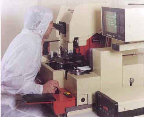
25 Nesting Tolerance Design rules during mask layout depend on nesting tolerance: δ A,B : Δ : n : uncertainty in feature size for mask level A and B alignment (or overlay) error between A and B number of alignment levels Minimum separation between level A and B = 3σ values usually given (99%) n 2 2 A 2 B (VLSI p. 472 ) Total 3σ must consider overlay error, magnification error, lens distortion, stepper-tostepper error, and reticle error (registration and linewidth) Inspection and linewidth measurement of resist patterns by CD SEM (CD = critical dimension) 25
 High-frequency")


26 Mask engineering 1. Optical Proximity Correction (OPC) High-frequency components of the diffracted light is lost because of finite apertures, circular lenses etc Ends and bows of narrow lines are not ideal OPC: Clever mask engineering based on software algorithms can compensate some of this error: Rule-based OPC Model-based OPC 26

27 Mask engineering 1. Optical Proximity Correction (OPC) Examples 27

")
28 Mask engineering 1. Optical Proximity Correction (OPC) Examples 28
29 Mask engineering 2. Phase shifting masks (PSM) Introducing material which shifts the light by 180 for adjacent mask patterns barely resolved improved resolution Intensity (Electrical amplitude) 2 (Plummer p. 233 ) 29
30 Concept Test Moore s law and the ITRS dictate that further scaling in the semiconductor industry is needed. The following options contribute to further scaling. A. High resolution lithography only works in the front end of the line (FEOL) because the depth of focus is limited. B. Chemical Mechanical Polishing (CMP) is a method to enhance lithography resolution. C. Optical Proximity Correction (OPC) uses models to predict changes in device behavior due to diffraction. D. Atomic Layer Deposition (ALD) enables the deposition of smooth films on the atomic scale, reducing some of the issues of lithography. E. Selective epitaxy can be used in the BEOL to smooth surface topography and enhance resolution of lithography. 30
31 Lithography Introduction Process Flow Wafer Exposure Systems Masks Resists State of the Art Lithography Next Generation Lithography (NGL) 31
32 Resist Technology Spin Curves Plot of spin speed versus film thickness Actual results will vary: equipment, environment, process and application specific Additional resist dilution to obtain other film thicknesses Source: MicroChem NanoPMMA data sheet 32
33 Resist Technology Positive and negative resist: Solubility in developer after light exposure is increased for positive resist decreased for negative resist Negative resist uncommon today because of positive limited resolution negative The resist is composed of: Resin, usually novolac Solvent Photoactive compound (PAC) 33
34 Contrast of Resist Contrast is experimentally determined D 0 : onset of exposure effect D f : dose at which exposure is complete High high resolution = F(process conditions) 1 log 10 D f D 0 Chemical amplification steepens transition in DUV resists DNQ (g-line, i-line): = 2-3, D f = 100 mjcm -2 Deep UV (DUV): = 5-10, D f = mjcm -2 34
 The CMTF for resists is defined as D f D0 CMTFresist D D f 0 10 10 1 1 1 1 DNQ (g-line, i-line): CMTF ~ 0.")
35 Critical Modulation Transfer Function (CMTF) The aerial image and the resist contrast in combination, result in the quality of the latent image produced. (Gray area is partially exposed area which determines the resist edge sharpness.) The CMTF for resists is defined as D f D0 CMTFresist D D f DNQ (g-line, i-line): CMTF ~ 0.4 Deep UV (DUV): CMTF ~ Sharp areal image Steep resist profile Poor areal image Resulting gradual profile 35
 prior to resist")
36 Effects of Standing Waves on Patterns Standing waves a problem, in particular when exposing on reflective layers such as metals Suppressed by antireflective coating (ARC) prior to resist spinning 36


37 Effects of Standing Waves on Patterns Photo courtesy of A. Vladar and P. Rissman, Hewlett Packard 37
38 Resist Process Integration 1. Lift-off Avoid etching of difficult materials Requires cold deposit process! Not suitable for CMOS production ( Sze p. 441 ) 38
 Patterning is made in upper layer.")
39 Resist Process Integration 2. Multilayer resist processing Under development for VLSI Example tri-layer resist: ( Wolf p. 424 ) Patterning is made in upper layer. This is used as a contact mask for the lower layer RIE (O 2 ) of polymer in (c) can be replaced by flood exposure 39


40 Resist Process Integration 3. Bilayer Resist Application: low-resistance gate electrodes for RF devices Mushroom or T-gates 40
41 Resist Process Integration 4. Image reversal of positive resist Exposed resist can be chemically altered by amine vapors to become non-dissolvable Flood exposure + development reverses image 41
42 Lithography Introduction Process Flow Wafer Exposure Systems Masks Resists State of the Art Lithography Next Generation Lithography (NGL) 42
43 State of the art lithography Current DUV generation (in ~2007): DUV 193 nm By combinations of phase-shift masks and off-axis illumination, 193 nm DUV can be extended beyond 100 nm, probably 70 nm! DUV 157 nm A solution for nm but large absorption makes refractive systems extremely difficult to design. Further, no resist technology exists. 43
44 Fraunhofer Diffraction: Improving Resolution Resolution R Practical resolution: R k1 where 0.6 < k 1 < 0.8 NA Improve resolution by reducing λ or increasing NA: Higher NA lenses also decrease the depth of focus NA = n sinα n is index of refraction of the material between wafer and lens Can we replace air (n = 1)? 44
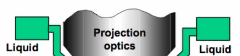

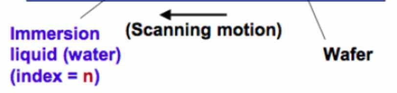
45 State-of-the-Art: Immersion Lithography 45
46 State-of-the-Art: Immersion Lithography 46
47 Lithography Introduction Process Flow Wafer Exposure Systems Masks Resists State of the Art Lithography Next Generation Lithography (NGL) 47
48 Next Generation Lithography (NGL): 2012 and beyond 1. Extreme UV lithography (EUV) 2. E-beam projection lithography (EPL) 3. Ion projection lithography 4. X-ray lithography 5. Nano Imprint Lithography (NIL) No consensus exists about the winner! It is very likely that it will be either EUV or EPL. Largest problem for all technologies is mask design! Possibly, mix-and-match strategies will be used (different litho technologies in the same process) In sharp contrast to 20 years common belief, it now appears that lithography will not act as "the show-stopper" for Moore's law! 48
 and as mask Strong support from US and European manufactures ASML predicts one system will cost 30 MUSD ( Plummer p278")
49 1. Extreme UV lithography (EUV) Light source with λ = 13 nm Purely reflecting system including mask Each mirror consists of multilayers of Mo and Si and can both be used for reduction (usually 4x) and as mask Strong support from US and European manufactures ASML predicts one system will cost 30 MUSD ( Plummer p278 ) 49
50 2. E-beam projection lithography (EPL) Electrons with λ < 0.1 nm. (Almost) no diffraction limit! EPL is a variation of e-beam lithography (EBL) which traditionally is used for direct writing (i.e. mask-less): Reticles, prototype chips, research etc Problem with EBL Throughput typically 50x lower than optical lithography. Beam size (shape) and scan schemes important: 50

51 2. E-beam projection lithography (EPL) SCALPEL (scattering with angular limitation e-beam lithography) Invented by Bell 1989 Membrane mask design in SCALPEL based on the various amount of scattering experienced by incoming electrons: Widely scattered electrons do not expose resist Simpler mask than EUV 4:1 system Large DOF DUV resists ( Plummer p. 275 ) 100 kev beam 51
52 3. Ion projection lithography Ions scatter much less than e- higher resolution and throughput than e-beam lithography Problems: Ion beam source Beam forming Mask Example on lithography system using Ga ions without mask: Reticle design based on a 0.5 μm thick stencil mask. Fragile! Ion beam of protons or H 2. A relatively immature technology compared to EPL. ( Chang p 322 ) 52
 Helium Ion Microscope: A new")

53 3. Ion projection lithography (Example) Helium Ion Microscope: A new Nano-Fabrication-Tool Zeiss Orion He Ion Microscope Spot size: d = 30 kev 53
")


54 IH2655 Spring Ion projection lithography (Example) Helium Ion Microscope: A new Nano-Fabrication-Tool graphene SiO2 150 nm Harvard Logo ingnr Graphene suspended Lemme et al., ACS Nano, Sub (unpublished) 10nm resolution 54
55 4. X-ray lithography X-rays with λ ~1 nm X-ray source usually a synchrotron connected to several X-ray steppers in litho area Focusing x-rays very difficult Proximity printing combined with step- and repeat action 1:1 system Very high resolution (no diffraction) and throughput Mask design requires absorbent and transparent regions. This has turned out extremely difficult for x-ray lithography Despite huge efforts, X-ray lithography now seems abandoned as NGL ( Chang p 314 ) 55
 + Precision + Random patterns - Reproducibility - Tilting - Contamination (contact with resist) Etching of residual resist and structuring by RIE")
56 5. Nanoimprint Lithography (NIL) Here: UV-NIL, also: thermal NIL Process Spin coating of imprint resists on Sisubstrate Template Pressing template into resist (< 1bar) UVcuring Detachment Resist UV light 365 nm Substrate + Low cost of ownership (COO) + Precision + Random patterns - Reproducibility - Tilting - Contamination (contact with resist) Etching of residual resist and structuring by RIE 56


57 5. Nanoimprint Lithography Example 1: J. Gutenberg nm SiO 2 Template 1452: Printing of first page of the Bible ( Gutenberg Bible ) 550 years later in 2002: Gutenberg Bible page, printed and etched into silicon, minimim features ~25 nm. Deutsches Museum, München, SEM images 57


58 5. Nanoimprint Lithography Example 2: Demonstration of UV-NIL in a MOSFET Triple-Gate Transistor made using NIL 0,04 3,5 V I DS / A 0,02 0, U DS / V 3,0 V 2,5 V 2,0 V Output characteristics SEM image Smallest features: <20nm Alignment: <20nm Fuchs et al., J. Vac. Sci. Technol. B, 24(6), 2006 AFM image 58
Lecture 13 Basic Photolithography
 Lecture 13 Basic Photolithography Chapter 12 Wolf and Tauber 1/64 Announcements Homework: Homework 3 is due today, please hand them in at the front. Will be returned one week from Thursday (16 th Nov).
Section 2: Lithography. Jaeger Chapter 2 Litho Reader. The lithographic process
 Section 2: Lithography Jaeger Chapter 2 Litho Reader The lithographic process Photolithographic Process (a) (b) (c) (d) (e) (f) (g) Substrate covered with silicon dioxide barrier layer Positive photoresist
Lecture 7. Lithography and Pattern Transfer. Reading: Chapter 7
 Lecture 7 Lithography and Pattern Transfer Reading: Chapter 7 Used for Pattern transfer into oxides, metals, semiconductors. 3 types of Photoresists (PR): Lithography and Photoresists 1.) Positive: PR
Section 2: Lithography. Jaeger Chapter 2 Litho Reader. EE143 Ali Javey Slide 5-1
 Section 2: Lithography Jaeger Chapter 2 Litho Reader EE143 Ali Javey Slide 5-1 The lithographic process EE143 Ali Javey Slide 5-2 Photolithographic Process (a) (b) (c) (d) (e) (f) (g) Substrate covered
MICROCHIP MANUFACTURING by S. Wolf
 MICROCHIP MANUFACTURING by S. Wolf Chapter 19 LITHOGRAPHY II: IMAGE-FORMATION and OPTICAL HARDWARE 2004 by LATTICE PRESS CHAPTER 19 - CONTENTS Preliminaries: Wave- Motion & The Behavior of Light Resolution
5. Lithography. 1. photolithography intro: overall, clean room 2. principle 3. tools 4. pattern transfer 5. resolution 6. next-gen
 5. Lithography 1. photolithography intro: overall, clean room 2. principle 3. tools 4. pattern transfer 5. resolution 6. next-gen References: Semiconductor Devices: Physics and Technology. 2 nd Ed. SM
Lithography. 3 rd. lecture: introduction. Prof. Yosi Shacham-Diamand. Fall 2004
 Lithography 3 rd lecture: introduction Prof. Yosi Shacham-Diamand Fall 2004 1 List of content Fundamental principles Characteristics parameters Exposure systems 2 Fundamental principles Aerial Image Exposure
Part 5-1: Lithography
 Part 5-1: Lithography Yao-Joe Yang 1 Pattern Transfer (Patterning) Types of lithography systems: Optical X-ray electron beam writer (non-traditional, no masks) Two-dimensional pattern transfer: limited
Lecture 5. Optical Lithography
 Lecture 5 Optical Lithography Intro For most of microfabrication purposes the process (e.g. additive, subtractive or implantation) has to be applied selectively to particular areas of the wafer: patterning
ECSE 6300 IC Fabrication Laboratory Lecture 3 Photolithography. Lecture Outline
 ECSE 6300 IC Fabrication Laboratory Lecture 3 Photolithography Prof. James J. Q. Lu Bldg. CII, Rooms 6229 Rensselaer Polytechnic Institute Troy, NY 12180 Tel. (518)276 2909 e mails: luj@rpi.edu http://www.ecse.rpi.edu/courses/s18/ecse
Section 2: Lithography. Jaeger Chapter 2. EE143 Ali Javey Slide 5-1
 Section 2: Lithography Jaeger Chapter 2 EE143 Ali Javey Slide 5-1 The lithographic process EE143 Ali Javey Slide 5-2 Photolithographic Process (a) (b) (c) (d) (e) (f) (g) Substrate covered with silicon
EE143 Fall 2016 Microfabrication Technologies. Lecture 3: Lithography Reading: Jaeger, Chap. 2
 EE143 Fall 2016 Microfabrication Technologies Lecture 3: Lithography Reading: Jaeger, Chap. 2 Prof. Ming C. Wu wu@eecs.berkeley.edu 511 Sutardja Dai Hall (SDH) 1-1 The lithographic process 1-2 1 Photolithographic
Optical Lithography. Keeho Kim Nano Team / R&D DongbuAnam Semi
 Optical Lithography Keeho Kim Nano Team / R&D DongbuAnam Semi Contents Lithography = Photolithography = Optical Lithography CD : Critical Dimension Resist Pattern after Development Exposure Contents Optical
Photolithography I ( Part 1 )
") 1 Photolithography I ( Part 1 ) Chapter 13 : Semiconductor Manufacturing Technology by M. Quirk & J. Serda Bjørn-Ove Fimland, Department of Electronics and Telecommunication, Norwegian University of Science
1 Photolithography I ( Part 1 ) Chapter 13 : Semiconductor Manufacturing Technology by M. Quirk & J. Serda Bjørn-Ove Fimland, Department of Electronics and Telecommunication, Norwegian University of Science
Semiconductor Manufacturing Technology. Semiconductor Manufacturing Technology. Photolithography: Resist Development and Advanced Lithography
 Semiconductor Manufacturing Technology Michael Quirk & Julian Serda October 2001 by Prentice Hall Chapter 15 Photolithography: Resist Development and Advanced Lithography Eight Basic Steps of Photolithography
Process Optimization
 Process Optimization Process Flow for non-critical layer optimization START Find the swing curve for the desired resist thickness. Determine the resist thickness (spin speed) from the swing curve and find
Photolithography. References: Introduction to Microlithography Thompson, Willson & Bowder, 1994
 Photolithography References: Introduction to Microlithography Thompson, Willson & Bowder, 1994 Microlithography, Science and Technology Sheats & Smith, 1998 Any other Microlithography or Photolithography
Photolithography II ( Part 2 )
") 1 Photolithography II ( Part 2 ) Chapter 14 : Semiconductor Manufacturing Technology by M. Quirk & J. Serda Saroj Kumar Patra, Department of Electronics and Telecommunication, Norwegian University of Science
1 Photolithography II ( Part 2 ) Chapter 14 : Semiconductor Manufacturing Technology by M. Quirk & J. Serda Saroj Kumar Patra, Department of Electronics and Telecommunication, Norwegian University of Science
PHGN/CHEN/MLGN 435/535: Interdisciplinary Silicon Processing Laboratory. Simple Si solar Cell!
 Where were we? Simple Si solar Cell! Two Levels of Masks - photoresist, alignment Etch and oxidation to isolate thermal oxide, deposited oxide, wet etching, dry etching, isolation schemes Doping - diffusion/ion
Major Fabrication Steps in MOS Process Flow
 Major Fabrication Steps in MOS Process Flow UV light Mask oxygen Silicon dioxide photoresist exposed photoresist oxide Silicon substrate Oxidation (Field oxide) Photoresist Coating Mask-Wafer Alignment
Outline. 1 Introduction. 2 Basic IC fabrication processes. 3 Fabrication techniques for MEMS. 4 Applications. 5 Mechanics issues on MEMS MDL NTHU
 Outline 1 Introduction 2 Basic IC fabrication processes 3 Fabrication techniques for MEMS 4 Applications 5 Mechanics issues on MEMS 2.2 Lithography Reading: Runyan Chap. 5, or 莊達人 Chap. 7, or Wolf and
Optical Lithography. Here Is Why. Burn J. Lin SPIE PRESS. Bellingham, Washington USA
 Optical Lithography Here Is Why Burn J. Lin SPIE PRESS Bellingham, Washington USA Contents Preface xiii Chapter 1 Introducing Optical Lithography /1 1.1 The Role of Lithography in Integrated Circuit Fabrication
Chapter 6. Photolithography
 Chapter 6 Photolithography 2006/4/10 1 Objectives List the four components of the photoresist Describe the difference between +PR and PR Describe a photolithography process sequence List four alignment
Photolithography 光刻 Part I: Optics
 微纳光电子材料与器件工艺原理 Photolithography 光刻 Part I: Optics Xing Sheng 盛兴 Department of Electronic Engineering Tsinghua University xingsheng@tsinghua.edu.cn 1 Integrate Circuits Moore's law transistor number transistor
Device Fabrication: Photolithography
 Device Fabrication: Photolithography 1 Objectives List the four components of the photoresist Describe the difference between +PR and PR Describe a photolithography process sequence List four alignment
State-of-the-art device fabrication techniques
 State-of-the-art device fabrication techniques! Standard Photo-lithography and e-beam lithography! Advanced lithography techniques used in semiconductor industry Deposition: Thermal evaporation, e-gun
EE-527: MicroFabrication
 EE-57: MicroFabrication Exposure and Imaging Photons white light Hg arc lamp filtered Hg arc lamp excimer laser x-rays from synchrotron Electrons Ions Exposure Sources focused electron beam direct write
Module 11: Photolithography. Lecture 14: Photolithography 4 (Continued)
") Module 11: Photolithography Lecture 14: Photolithography 4 (Continued) 1 In the previous lecture, we have discussed the utility of the three printing modes, and their relative advantages and disadvantages.
Module 11: Photolithography Lecture 14: Photolithography 4 (Continued) 1 In the previous lecture, we have discussed the utility of the three printing modes, and their relative advantages and disadvantages.
Micro- and Nano-Technology... for Optics
 Micro- and Nano-Technology...... for Optics 3.2 Lithography U.D. Zeitner Fraunhofer Institut für Angewandte Optik und Feinmechanik Jena Printing on Stones Map of Munich Stone Print Contact Printing light
MICRO AND NANOPROCESSING TECHNOLOGIES
 MICRO AND NANOPROCESSING TECHNOLOGIES LECTURE 4 Optical lithography Concepts and processes Lithography systems Fundamental limitations and other issues Photoresists Photolithography process Process parameter
Clean Room Technology Optical Lithography. Lithography I. takenfrombdhuey
 Clean Room Technology Optical Lithography Lithography I If the automobile had followed the same development cycle as the computer, a Rolls Royce would today cost $100, get a million miles per gallon, and
Lithography Is the Designer s Brush. Lithography is indispensible for defining locations and configurations of circuit elements/functions.
 Lithography 1 Lithography Is the Designer s Brush Lithography is indispensible for defining locations and configurations of circuit elements/functions. 2 ITRS 2007 The major challenge in litho: CD, CD
Micro- and Nano-Technology... for Optics
 Micro- and Nano-Technology...... for Optics 3.2 Lithography U.D. Zeitner Fraunhofer Institut für Angewandte Optik und Feinmechanik Jena Printing on Stones Map of Munich Stone Print Shadow Printing Photomask
Module - 2 Lecture - 13 Lithography I
 Nano Structured Materials-Synthesis, Properties, Self Assembly and Applications Prof. Ashok. K.Ganguli Department of Chemistry Indian Institute of Technology, Delhi Module - 2 Lecture - 13 Lithography
EE 143 Microfabrication Technology Fall 2014
 EE 143 Microfabrication Technology Fall 2014 Prof. Clark T.-C. Nguyen Dept. of Electrical Engineering & Computer Sciences University of California at Berkeley Berkeley, CA 94720 EE 143: Microfabrication
What s So Hard About Lithography?
 What s So Hard About Lithography? Chris A. Mack, www.lithoguru.com, Austin, Texas Optical lithography has been the mainstay of semiconductor patterning since the early days of integrated circuit production.
Photolithography Technology and Application
 Photolithography Technology and Application Jeff Tsai Director, Graduate Institute of Electro-Optical Engineering Tatung University Art or Science? Lind width = 100 to 5 micron meter!! Resolution = ~ 3
Dr. Dirk Meyners Prof. Wagner. Wagner / Meyners Micro / Nanosystems Technology
 Micro/Nanosystems Technology Dr. Dirk Meyners Prof. Wagner 1 Outline - Lithography Overview - UV-Lithography - Resolution Enhancement Techniques - Electron Beam Lithography - Patterning with Focused Ion
Lithography. Development of High-Quality Attenuated Phase-Shift Masks
 Lithography S P E C I A L Development of High-Quality Attenuated Phase-Shift Masks by Toshihiro Ii and Masao Otaki, Toppan Printing Co., Ltd. Along with the year-by-year acceleration of semiconductor device
DOE Project: Resist Characterization
 DOE Project: Resist Characterization GOAL To achieve high resolution and adequate throughput, a photoresist must possess relatively high contrast and sensitivity to exposing radiation. The objective of
Mask Technology Development in Extreme-Ultraviolet Lithography
 Mask Technology Development in Extreme-Ultraviolet Lithography Anthony Yen September 6, 2013 Projected End of Optical Lithography 2013 TSMC, Ltd 1976 1979 1982 1985 1988 1991 1994 1997 2000 2003 2007 2012
Copyright 2000 by the Society of Photo-Optical Instrumentation Engineers.
 Copyright by the Society of Photo-Optical Instrumentation Engineers. This paper was published in the proceedings of Optical Microlithography XIII, SPIE Vol. 4, pp. 658-664. It is made available as an electronic
Nanotechnology I+II 2006 / 07
 Nanotechnology for engineers Winter semester 2006-2007 Nanotechnology I+II 2006 / 07 Juergen Brugger & Patrik Hoffmann & Teams Course agenda (winter semester) Nanotechnology I winter semester (23.10.06-9.2.06)
Optical Issues in Photolithography
 OpenStax-CNX module: m25448 1 Optical Issues in Photolithography Andrew R. Barron This work is produced by OpenStax-CNX and licensed under the Creative Commons Attribution License 3.0 note: This module
Optolith 2D Lithography Simulator
 2D Lithography Simulator Advanced 2D Optical Lithography Simulator 4/13/05 Introduction is a powerful non-planar 2D lithography simulator that models all aspects of modern deep sub-micron lithography It
Chapter 6 Photolithography
 Chapter 6 Photolithography Hong Xiao, Ph. D. hxiao89@hotmail.com www2.austin.cc.tx.us/hongxiao/book.htm Hong Xiao, Ph. D. www2.austin.cc.tx.us/hongxiao/book.htm 1 Objectives List the four components of
UV Nanoimprint Stepper Technology: Status and Roadmap. S.V. Sreenivasan Sematech Litho Forum May 14 th, 2008
 UV Nanoimprint Stepper Technology: Status and Roadmap S.V. Sreenivasan Sematech Litho Forum May 14 th, 2008 Overview Introduction Stepper technology status: Patterning and CD Control Through Etch Alignment
Micro/Nanolithography
 Dale E. Ewbank dale.ewbank@rit.edu unl081413_microe.ppt 2013 Dale E. Ewbank page 1 OUTLINE Masks Optical Lithography Photoresist Sensitivity Processing Exposure Tools Advanced Processes page 2 MICROLITHOGRAPHY
TECHNOLOGY ROADMAP 2006 UPDATE LITHOGRAPHY FOR
 INTERNATIONAL TECHNOLOGY ROADMAP FOR SEMICONDUCTORS 2006 UPDATE LITHOGRAPHY THE ITRS IS DEVISED AND INTENDED FOR TECHNOLOGY ASSESSMENT ONLY AND IS WITHOUT REGARD TO ANY COMMERCIAL CONSIDERATIONS PERTAINING
Copyright 2000, Society of Photo-Optical Instrumentation Engineers This paper was published in Optical Microlithography XIII, Volume 4000 and is made
 Copyright 00, Society of Photo-Optical Instrumentation Engineers This paper was published in Optical Microlithography XIII, Volume 4000 and is made available as an electronic reprint with permission of
immersion optics Immersion Lithography with ASML HydroLith TWINSCAN System Modifications for Immersion Lithography by Bob Streefkerk
 immersion optics Immersion Lithography with ASML HydroLith by Bob Streefkerk For more than 25 years, many in the semiconductor industry have predicted the end of optical lithography. Recent developments,
Nanoscale Lithography. NA & Immersion. Trends in λ, NA, k 1. Pushing The Limits of Photolithography Introduction to Nanotechnology
 15-398 Introduction to Nanotechnology Nanoscale Lithography Seth Copen Goldstein Seth@cs.cmu.Edu CMU Pushing The Limits of Photolithography Reduce wavelength (λ) Use Reducing Lens Increase Numerical Aperture
Optical Microlithography XXVIII
 PROCEEDINGS OF SPIE Optical Microlithography XXVIII Kafai Lai Andreas Erdmann Editors 24-26 February 2015 San Jose, California, United States Sponsored by SPIE Cosponsored by Cymer, an ASML company (United
FABRICATION OF CMOS INTEGRATED CIRCUITS. Dr. Mohammed M. Farag
 FABRICATION OF CMOS INTEGRATED CIRCUITS Dr. Mohammed M. Farag Outline Overview of CMOS Fabrication Processes The CMOS Fabrication Process Flow Design Rules Reference: Uyemura, John P. "Introduction to
Development of Nanoimprint Mold Using JBX-9300FS
 Development of Nanoimprint Mold Using JBX-9300FS Morihisa Hoga, Mikio Ishikawa, Naoko Kuwahara Tadahiko Takikawa and Shiho Sasaki Dai Nippon Printing Co., Ltd Research & Development Center Electronic Device
T in sec, I in W/cm 2, E in J/cm 2
 Exposures from Mask Aligner into Resist Mask aligner images created by shadowing from mask into resist Soft contact and Proximity good for 3 micron structures Vacuum Hard Contact: no shadow effects at
Microlithography. Dale E. Ewbank ul ppt. Microlithography Dale E. Ewbank page 1
 Dale E. Ewbank dale.ewbank@rit.edu ul012014.ppt 2014 Dale E. Ewbank page 1 OUTLINE Masks Optical Lithography Photoresist Sensitivity Processing Exposure Tools Advanced Processes page 2 MICROLITHOGRAPHY
Chapter 2 Silicon Planar Processing and Photolithography
 Chapter 2 Silicon Planar Processing and Photolithography The success of the electronics industry has been due in large part to advances in silicon integrated circuit (IC) technology based on planar processing,
T in sec, I in W/cm 2, E in J/cm 2
 Exposures from Mask Aligner into Resist Mask aligner images created by shadowing from mask into resist Soft contact and Proximity good for 3 micron structures Vacuum Hard Contact: no shadow effects at
NANOFABRICATION, THE NEW GENERATION OF LITHOGRAPHY. Cheng-Sheng Huang & Alvin Chang ABSTRACT
 NANOFABRICATION, THE NEW GENERATION OF LITHOGRAPHY Cheng-Sheng Huang & Alvin Chang ABSTRACT Fabrication on the micro- and nano-structure has opened the new horizons in science and engineering. The success
T in sec, I in W/cm 2, E in J/cm 2
 Exposures from Mask Aligner into Resist Mask aligner images created by shadowing from mask into resist Soft contact and Proximity good for 3 micron structures Vacuum Hard Contact: no shadow effects at
Lithographic Performance and Mix-and-Match Lithography using 100 kv Electron Beam System JBX-9300FS
 Lithographic Performance and Mix-and-Match Lithography using 100 kv Electron Beam System JBX-9300FS Yukinori Ochiai, Takashi Ogura, Mitsuru Narihiro, and Kohichi Arai Silicon Systems Research Laboratories,
k λ NA Resolution of optical systems depends on the wavelength visible light λ = 500 nm Extreme ultra-violet and soft x-ray light λ = 1-50 nm
 Resolution of optical systems depends on the wavelength visible light λ = 500 nm Spatial Resolution = k λ NA EUV and SXR microscopy can potentially resolve full-field images with 10-100x smaller features
INTERNATIONAL TECHNOLOGY ROADMAP SEMICONDUCTORS 2001 EDITION LITHOGRAPHY FOR
 INTERNATIONAL TECHNOLOGY ROADMAP FOR SEMICONDUCTORS 2001 EDITION LITHOGRAPHY TABLE OF CONTENTS Scope...1 Difficult Challenges...1 Lithography Technology Requirements...3 Potential Solutions...14 Crosscut
MicroSpot FOCUSING OBJECTIVES
 OFR P R E C I S I O N O P T I C A L P R O D U C T S MicroSpot FOCUSING OBJECTIVES APPLICATIONS Micromachining Microlithography Laser scribing Photoablation MAJOR FEATURES For UV excimer & high-power YAG
Holistic View of Lithography for Double Patterning. Skip Miller ASML
 Holistic View of Lithography for Double Patterning Skip Miller ASML Outline Lithography Requirements ASML Holistic Lithography Solutions Conclusions Slide 2 Shrink Continues Lithography keeps adding value
Institute of Solid State Physics. Technische Universität Graz. Lithography. Peter Hadley
 Technische Universität Graz Institute of Solid State Physics Lithography Peter Hadley http://www.cleanroom.byu.edu/virtual_cleanroom.parts/lithography.html http://www.cleanroom.byu.edu/su8.phtml Spin coater
Microlithography. exposing radiation. mask. imaging system (low pass filter) photoresist. develop. etch
 photoresist. develop. etch") Microlithography Geometry Trends Master Patterns: Mask technology Pattern Transfer: Mask Aligner technology Wafer Transfer Media: Photo resist technology mask blank: transparent, mechanically rigid masking
Microlithography Geometry Trends Master Patterns: Mask technology Pattern Transfer: Mask Aligner technology Wafer Transfer Media: Photo resist technology mask blank: transparent, mechanically rigid masking
Tutor43.doc; Version 8/15/03 T h e L i t h o g r a p h y E x p e r t (November 2003)
") Tutor43.doc; Version /15/03 T h e L i t h o g r a p h y E x p e r t (November 2003) Scattering Bars Chris A. Mack, KLA-Tencor, FINLE Division, Austin, Texas Resolution enhancement technologies refer to
Tutor43.doc; Version /15/03 T h e L i t h o g r a p h y E x p e r t (November 2003) Scattering Bars Chris A. Mack, KLA-Tencor, FINLE Division, Austin, Texas Resolution enhancement technologies refer to
BI-LAYER DEEP UV RESIST SYSTEM. Mark A. Boehm 5th Year Microelectronic Engineering Student Rochester Institute of Technology ABSTRACT
 INTRODUCTION BI-LAYER DEEP UV RESIST SYSTEM Mark A. Boehm 5th Year Microelectronic Engineering Student Rochester Institute of Technology ABSTRACT A portable conformable mask (PCM) system employing KTIS2O
CHAPTER 2 Principle and Design
 CHAPTER 2 Principle and Design The binary and gray-scale microlens will be designed and fabricated. Silicon nitride and photoresist will be taken as the material of the microlens in this thesis. The design
Optical Projection Printing and Modeling
 Optical Projection Printing and Modeling Overview of optical lithography, concepts, trends Basic Parameters and Effects (1-14) Resolution Depth of Focus; Proximity, MEEF, LES Image Calculation, Characterization
TECHNOLOGY ROADMAP 2005 EDITION LITHOGRAPHY FOR
 INTERNATIONAL TECHNOLOGY ROADMAP FOR SEMICONDUCTORS 2005 EDITION LITHOGRAPHY THE ITRS IS DEVISED AND INTENDED FOR TECHNOLOGY ASSESSMENT ONLY AND IS WITHOUT REGARD TO ANY COMMERCIAL CONSIDERATIONS PERTAINING
2009 International Workshop on EUV Lithography
 Contents Introduction Absorber Stack Optimization Non-flatness Correction Blank Defect and Its Mitigation Wafer Printing Inspection Actinic Metrology Cleaning and Repair Status Remaining Issues in EUV
Photolithography Module
 Electronics Workforce Development System Photolithography Module Introduction Photolithography Module This module will teach students the different types of microlithographic systems being used today,
Inspection of templates for imprint lithography
 Inspection of templates for imprint lithography Harald F. Hess, a) Don Pettibone, David Adler, and Kirk Bertsche KLA-Tencor 160 Rio Robles, San Jose, California 95134 Kevin J. Nordquist, David P. Mancini,
Strategies for low cost imprint molds
 Strategies for low cost imprint molds M.P.C. Watts, Impattern Solutions, 9404 Bell Mountain Drive Austin TX 78730 www.impattern.com ABSTRACT The Cost of ownership (COO) due to the mold can be minimized
3.Photolithography and resist systems
 3.Photolithography and resist systems Exposure Mercury arc lamp Shadow printing projection printing Photomask Substrates Resist systems DNQ-Novolak-based Epoxy-based Polyimide based 1 Exposure Mercury
A review on contemporary practices in Lithography
 IOSR Journal of Applied Chemistry (IOSR-JAC) e-issn: 2278-5736.Volume 7, Issue 4 Ver. II. (Apr. 2014), PP 27-31 A review on contemporary practices in Lithography Perna Kishor Krishna, Mantha Anil Srimanth,
Feature-level Compensation & Control
 Feature-level Compensation & Control 2 Sensors and Control Nathan Cheung, Kameshwar Poolla, Costas Spanos Workshop 11/19/2003 3 Metrology, Control, and Integration Nathan Cheung, UCB SOI Wafers Multi wavelength
Optical Requirements
 Optical Requirements Transmission vs. Film Thickness A pellicle needs a good light transmission and long term transmission stability. Transmission depends on the film thickness, film material and any anti-reflective
Update on 193nm immersion exposure tool
 Update on 193nm immersion exposure tool S. Owa, H. Nagasaka, Y. Ishii Nikon Corporation O. Hirakawa and T. Yamamoto Tokyo Electron Kyushu Ltd. January 28, 2004 Litho Forum 1 What is immersion lithography?
Reducing Proximity Effects in Optical Lithography
 INTERFACE '96 This paper was published in the proceedings of the Olin Microlithography Seminar, Interface '96, pp. 325-336. It is made available as an electronic reprint with permission of Olin Microelectronic
Quantized patterning using nanoimprinted blanks
 IOP PUBLISHING Nanotechnology 20 (2009) 155303 (7pp) Quantized patterning using nanoimprinted blanks NANOTECHNOLOGY doi:10.1088/0957-4484/20/15/155303 Stephen Y Chou 1, Wen-Di Li and Xiaogan Liang NanoStructure
KrF EXCIMER LASER LITHOGRAPHY TECHNOLOGY FOR 64MDRAM
 Journa' of Photopolymer Science and Technology Volume 4, Number 3 (1991) 361-369 KrF EXCIMER LASER LITHOGRAPHY TECHNOLOGY FOR 64MDRAM MASAYUKI ENDO, YOSHIYUKI TAM, TOSHIKI YABU, SHOZO OKADA MASARU SASAGO
Micro- and Nano- Fabrication and Replication Techniques
 Micro- and Nano- Fabrication and Replication Techniques Why do we have to write thing small and replicate fast? Plenty of Room at the Bottom Richard P. Feynman, December 1959 How do we write it? We have
Semiconductor Technology
 Semiconductor Technology from A to Z + - x 1 0 x Photolithographie www.halbleiter.org Contents Contents List of Figures III 1 Photolithographie 1 1.1 Exposure and resist coating..........................
Contrast Enhancement Materials CEM 365HR
 INTRODUCTION In 1989 Shin-Etsu Chemical acquired MicroSi, Inc. including their Contrast Enhancement Material (CEM) technology business*. A concentrated effort in the technology advancement of a CEM led
i- Line Photoresist Development: Replacement Evaluation of OiR
 i- Line Photoresist Development: Replacement Evaluation of OiR 906-12 Nishtha Bhatia High School Intern 31 July 2014 The Marvell Nanofabrication Laboratory s current i-line photoresist, OiR 897-10i, has
* AIT-5: Maskless, High-NA, Immersion, EUV, Imprint
 Advanced Issues and Technology (AIT) Modules Purpose: Explain the top advanced issues and concepts in optical projection printing and electron-beam lithography. AIT-1: LER and CAR AIT-2: Resolution Enhancement
450mm patterning out of darkness Backend Process Exposure Tool SOKUDO Lithography Breakfast Forum July 10, 2013 Doug Shelton Canon USA Inc.
 450mm patterning out of darkness Backend Process Exposure Tool SOKUDO Lithography Breakfast Forum 2013 July 10, 2013 Doug Shelton Canon USA Inc. Introduction Half Pitch [nm] 2013 2014 2015 2016 2017 2018
Optical Waveguide Types
 8 Refractive Micro Optics Optical Waveguide Types There are two main types of optical waveguide structures: the step index and the graded index. In a step-index waveguide, the interface between the core
High-resolution microlithography using a 193nm excimer laser source. Nadeem H. Rizvi, Dominic Ashworth, Julian S. Cashmore and Malcolm C.
 High-resolution microlithography using a 193nm excimer laser source. Nadeem H. Rizvi, Dominic Ashworth, Julian S. Cashmore and Malcolm C. Gower Exitech Limited Hanborough Park, Long Hanborough, Oxford
EUV Substrate and Blank Inspection
 EUV Substrate and Blank Inspection SEMATECH EUV Workshop 10/11/99 Steve Biellak KLA-Tencor RAPID Division *This work is partially funded by NIST-ATP project 98-06, Project Manager Purabi Mazumdar 1 EUV
Advanced Digital Integrated Circuits. Lecture 2: Scaling Trends. Announcements. No office hour next Monday. Extra office hour Tuesday 2-3pm
 EE241 - Spring 20 Advanced Digital Integrated Circuits Lecture 2: Scaling Trends and Features of Modern Technologies Announcements No office hour next Monday Extra office hour Tuesday 2-3pm 2 1 Outline
Key Photolithographic Outputs
 Exposure latitude Depth of Focus Exposure latitude Vs DOF plot Linearity and MEEF Isolated-Dense Bias NILS Contrast Swing Curve Reflectivity Curve 1 Exposure latitude:the range of exposure energies (usually
Synthesis of projection lithography for low k1 via interferometry
 Synthesis of projection lithography for low k1 via interferometry Frank Cropanese *, Anatoly Bourov, Yongfa Fan, Andrew Estroff, Lena Zavyalova, Bruce W. Smith Center for Nanolithography Research, Rochester
OPC Rectification of Random Space Patterns in 193nm Lithography
 OPC Rectification of Random Space Patterns in 193nm Lithography Mosong Cheng, Andrew Neureuther, Keeho Kim*, Mark Ma*, Won Kim*, Maureen Hanratty* Department of Electrical Engineering and Computer Sciences
Analysis of Focus Errors in Lithography using Phase-Shift Monitors
 Draft paper for SPIE Conference on Microlithography (Optical Lithography) 6/6/2 Analysis of Focus Errors in Lithography using Phase-Shift Monitors Bruno La Fontaine *a, Mircea Dusa **b, Jouke Krist b,
ADVANCED TECHNOLOGY FOR EXTENDING OPTICAL LITHOGRAPHY
 ADVANCED TECHNOLOGY FOR EXTENDING OPTICAL LITHOGRAPHY Christian Wagner a, Winfried Kaiser a, Jan Mulkens b, Donis G. Flagello c a Carl Zeiss, D-73446 Oberkochen, Germany; b ASM Lithography, De Run 1110,