ECSE 6300 IC Fabrication Laboratory Lecture 3 Photolithography. Lecture Outline
|
|
|
- Carol Simpson
- 5 years ago
- Views:
Transcription
1 ECSE 6300 IC Fabrication Laboratory Lecture 3 Photolithography Prof. James J. Q. Lu Bldg. CII, Rooms 6229 Rensselaer Polytechnic Institute Troy, NY Tel. (518) e mails: luj@rpi.edu /index.html 3-1 Lecture Outline Photolithography Practice Photoresist Chemistry Contact and Proximity Printing Standing Wave Problem Geometric Optics Future Trends Topics Not Covered Note: The lecture slides were prepared based on the original materials written by Profs. T.P. Chow and J.-Q. Lu 3-4
2 Device Lithography Step 3-5 Exposure Techniques for Pattern Definition 3-6
3 Positive vs. Negative Photoresist 3-7 Photoresist Chemistry 3-8
 mask helps Global vs.")
4 Photoresist Development Dose = Time x Light Intensity 3-9 Mask to Wafer Alignment Particularly challenging for a dark field mask Use of iron oxide (semitransparent) mask helps Global vs. die by die alignment 3-10

5 Contact and Proximity Printing 3 Modes: Hard Contact (Vacuum needed) Soft Contact Proximity Printing g 20 to 50m Diffraction Minimum feature size resolved: W min kg k~1: constant 3-11 Q Parameter If << g <<W 2 / : 2 Q W g, g Q more faithful image Dotted curve: Diverging half angle = 1.5 /W rad. 3-12


6 Proximity Printing with Collimated and Uncollimated Light 3-13 Example of a Proximity Printer F: M: L: Filter Mirror Fly s eye lens 3-14


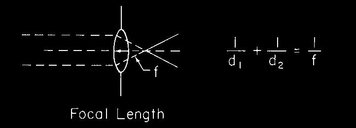
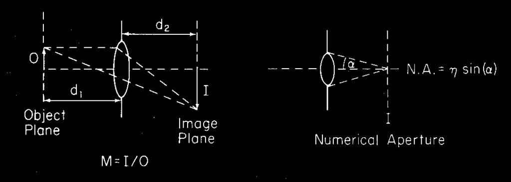
7 Standing Wave Problem Solution: Post exposure bake (PEB) Anti reflective Coating (PARC and BARC) Geometric Optics D N.A = n sin(α) = D/2f 3-16
 Depth of Focus: DoF k 2 Numerical Aperture and Depth of Focus NA 2 NA = n sin(α) =")
 NA = 0.")
8 Resolution: CD k1 NA (0.6 < k 1 < 0.8, depending on resist) Depth of Focus: DoF k 2 Numerical Aperture and Depth of Focus NA 2 NA = n sin(α) = D/2f 3-17 Transfer Function Comparison Spatial coherence of the system: Light Source Diameter S Condenser Lens Diameter Lens A NA = 0.28 S = 0.75 = 436 nm mask I MTF I max max - I I min min Lens B (Quartz) NA = 0.38 S = 1 = 248 nm 1 Feature size Lens B is capable of much higher resolution 3-18


9 Future Trend Photolithography has been counted out many times before, but.. Stable UV sources and mask cost are the two most formidable challenges Wrong Prediction*! *R.K. Watts, in VLSI Technology, Optical Projection Photolithography Step and Repeat Exposure Light source Reticle Reduction Optics Thermal Stability Alignment & Stage Stepping Throughput Light sources Simplified Stepper System 3-20
 Throughput (80 120 W/H) CD control (10% of nominal CD) Overlay (30% of the node) Resist issues Pellicles issues Economical challenges Mask cost and")
10 Light Sources for photolithography 546 nm e line 436 nm g line 405 nm h line 365 nm i line Mercury Lamp Output Intensity Kr = Krypton 3-21 What are the challenges for NGL? Technical challenges Resolution (<45 nm) Throughput ( W/H) CD control (10% of nominal CD) Overlay (30% of the node) Resist issues Pellicles issues Economical challenges Mask cost and fabrication delay $ K / mask (1st Year in production) and 3 5 months Manufacturing Cycle Times (<3 year/cycle)!! Equipment cost (>$10M for 193 nm, >$1M for lens) Equipment in time to market 3-22
 3-23 Immersion Lithography Lens")

 = D/2f http://www.eweek.")
11 Optical Engineering Optical Proximity Correction (OPC) Phase Shift Mask (PSM) 3-23 Immersion Lithography Lens 193 nm immersion Medium n Eqvl H 2 O nm Lens n Stage Water Wafer 157 nm dry CD k1 NA DoF k2 NA N nm 2 NA = n sin(α) = D/2f Infrastructure/New Features of AMDs 45nm Shanghai Processor 3-24
 Alpha Demo Tool a $65 million tool from ASML Source: College of")

12 EUV Lithography EUV Development: Forever Delayed? = 13.5 nm The world s first extreme ultraviolet (EUV) Alpha Demo Tool a $65 million tool from ASML Source: College of Nanoscale Science and Engineering (CNSE) of UAlbany Topics Not Covered Projection lithography: e beam, X ray and ion beam Stable UV light sources (e.g., KrF) Pellicles Bi and Tri layer Resist Contrast Enhanced Photolithography Master Mask Generation Nano imprinter 3-26
Lithography. 3 rd. lecture: introduction. Prof. Yosi Shacham-Diamand. Fall 2004
 Lithography 3 rd lecture: introduction Prof. Yosi Shacham-Diamand Fall 2004 1 List of content Fundamental principles Characteristics parameters Exposure systems 2 Fundamental principles Aerial Image Exposure
MICRO AND NANOPROCESSING TECHNOLOGIES
 MICRO AND NANOPROCESSING TECHNOLOGIES LECTURE 4 Optical lithography Concepts and processes Lithography systems Fundamental limitations and other issues Photoresists Photolithography process Process parameter
Photolithography I ( Part 1 )
") 1 Photolithography I ( Part 1 ) Chapter 13 : Semiconductor Manufacturing Technology by M. Quirk & J. Serda Bjørn-Ove Fimland, Department of Electronics and Telecommunication, Norwegian University of Science
1 Photolithography I ( Part 1 ) Chapter 13 : Semiconductor Manufacturing Technology by M. Quirk & J. Serda Bjørn-Ove Fimland, Department of Electronics and Telecommunication, Norwegian University of Science
Major Fabrication Steps in MOS Process Flow
 Major Fabrication Steps in MOS Process Flow UV light Mask oxygen Silicon dioxide photoresist exposed photoresist oxide Silicon substrate Oxidation (Field oxide) Photoresist Coating Mask-Wafer Alignment
Part 5-1: Lithography
 Part 5-1: Lithography Yao-Joe Yang 1 Pattern Transfer (Patterning) Types of lithography systems: Optical X-ray electron beam writer (non-traditional, no masks) Two-dimensional pattern transfer: limited
5. Lithography. 1. photolithography intro: overall, clean room 2. principle 3. tools 4. pattern transfer 5. resolution 6. next-gen
 5. Lithography 1. photolithography intro: overall, clean room 2. principle 3. tools 4. pattern transfer 5. resolution 6. next-gen References: Semiconductor Devices: Physics and Technology. 2 nd Ed. SM
Photolithography II ( Part 2 )
") 1 Photolithography II ( Part 2 ) Chapter 14 : Semiconductor Manufacturing Technology by M. Quirk & J. Serda Saroj Kumar Patra, Department of Electronics and Telecommunication, Norwegian University of Science
1 Photolithography II ( Part 2 ) Chapter 14 : Semiconductor Manufacturing Technology by M. Quirk & J. Serda Saroj Kumar Patra, Department of Electronics and Telecommunication, Norwegian University of Science
Lecture 7. Lithography and Pattern Transfer. Reading: Chapter 7
 Lecture 7 Lithography and Pattern Transfer Reading: Chapter 7 Used for Pattern transfer into oxides, metals, semiconductors. 3 types of Photoresists (PR): Lithography and Photoresists 1.) Positive: PR
Lecture 8. Microlithography
 Lecture 8 Microlithography Lithography Introduction Process Flow Wafer Exposure Systems Masks Resists State of the Art Lithography Next Generation Lithography (NGL) Recommended videos: http://www.youtube.com/user/asmlcompany#p/search/1/jh6urfqt_d4
EE143 Fall 2016 Microfabrication Technologies. Lecture 3: Lithography Reading: Jaeger, Chap. 2
 EE143 Fall 2016 Microfabrication Technologies Lecture 3: Lithography Reading: Jaeger, Chap. 2 Prof. Ming C. Wu wu@eecs.berkeley.edu 511 Sutardja Dai Hall (SDH) 1-1 The lithographic process 1-2 1 Photolithographic
Section 2: Lithography. Jaeger Chapter 2 Litho Reader. EE143 Ali Javey Slide 5-1
 Section 2: Lithography Jaeger Chapter 2 Litho Reader EE143 Ali Javey Slide 5-1 The lithographic process EE143 Ali Javey Slide 5-2 Photolithographic Process (a) (b) (c) (d) (e) (f) (g) Substrate covered
Chapter 6. Photolithography
 Chapter 6 Photolithography 2006/4/10 1 Objectives List the four components of the photoresist Describe the difference between +PR and PR Describe a photolithography process sequence List four alignment
Section 2: Lithography. Jaeger Chapter 2 Litho Reader. The lithographic process
 Section 2: Lithography Jaeger Chapter 2 Litho Reader The lithographic process Photolithographic Process (a) (b) (c) (d) (e) (f) (g) Substrate covered with silicon dioxide barrier layer Positive photoresist
Semiconductor Manufacturing Technology. Semiconductor Manufacturing Technology. Photolithography: Resist Development and Advanced Lithography
 Semiconductor Manufacturing Technology Michael Quirk & Julian Serda October 2001 by Prentice Hall Chapter 15 Photolithography: Resist Development and Advanced Lithography Eight Basic Steps of Photolithography
Optical Lithography. Keeho Kim Nano Team / R&D DongbuAnam Semi
 Optical Lithography Keeho Kim Nano Team / R&D DongbuAnam Semi Contents Lithography = Photolithography = Optical Lithography CD : Critical Dimension Resist Pattern after Development Exposure Contents Optical
Lecture 5. Optical Lithography
 Lecture 5 Optical Lithography Intro For most of microfabrication purposes the process (e.g. additive, subtractive or implantation) has to be applied selectively to particular areas of the wafer: patterning
Section 2: Lithography. Jaeger Chapter 2. EE143 Ali Javey Slide 5-1
 Section 2: Lithography Jaeger Chapter 2 EE143 Ali Javey Slide 5-1 The lithographic process EE143 Ali Javey Slide 5-2 Photolithographic Process (a) (b) (c) (d) (e) (f) (g) Substrate covered with silicon
Lecture 13 Basic Photolithography
 Lecture 13 Basic Photolithography Chapter 12 Wolf and Tauber 1/64 Announcements Homework: Homework 3 is due today, please hand them in at the front. Will be returned one week from Thursday (16 th Nov).
Optical Lithography. Here Is Why. Burn J. Lin SPIE PRESS. Bellingham, Washington USA
 Optical Lithography Here Is Why Burn J. Lin SPIE PRESS Bellingham, Washington USA Contents Preface xiii Chapter 1 Introducing Optical Lithography /1 1.1 The Role of Lithography in Integrated Circuit Fabrication
Device Fabrication: Photolithography
 Device Fabrication: Photolithography 1 Objectives List the four components of the photoresist Describe the difference between +PR and PR Describe a photolithography process sequence List four alignment
Process Optimization
 Process Optimization Process Flow for non-critical layer optimization START Find the swing curve for the desired resist thickness. Determine the resist thickness (spin speed) from the swing curve and find
Optical Requirements
 Optical Requirements Transmission vs. Film Thickness A pellicle needs a good light transmission and long term transmission stability. Transmission depends on the film thickness, film material and any anti-reflective
Photolithography 光刻 Part I: Optics
 微纳光电子材料与器件工艺原理 Photolithography 光刻 Part I: Optics Xing Sheng 盛兴 Department of Electronic Engineering Tsinghua University xingsheng@tsinghua.edu.cn 1 Integrate Circuits Moore's law transistor number transistor
Module 11: Photolithography. Lecture 14: Photolithography 4 (Continued)
") Module 11: Photolithography Lecture 14: Photolithography 4 (Continued) 1 In the previous lecture, we have discussed the utility of the three printing modes, and their relative advantages and disadvantages.
Module 11: Photolithography Lecture 14: Photolithography 4 (Continued) 1 In the previous lecture, we have discussed the utility of the three printing modes, and their relative advantages and disadvantages.
Optolith 2D Lithography Simulator
 2D Lithography Simulator Advanced 2D Optical Lithography Simulator 4/13/05 Introduction is a powerful non-planar 2D lithography simulator that models all aspects of modern deep sub-micron lithography It
Nanotechnology I+II 2006 / 07
 Nanotechnology for engineers Winter semester 2006-2007 Nanotechnology I+II 2006 / 07 Juergen Brugger & Patrik Hoffmann & Teams Course agenda (winter semester) Nanotechnology I winter semester (23.10.06-9.2.06)
Chapter 6 Photolithography
 Chapter 6 Photolithography Hong Xiao, Ph. D. hxiao89@hotmail.com www2.austin.cc.tx.us/hongxiao/book.htm Hong Xiao, Ph. D. www2.austin.cc.tx.us/hongxiao/book.htm 1 Objectives List the four components of
MICROCHIP MANUFACTURING by S. Wolf
 MICROCHIP MANUFACTURING by S. Wolf Chapter 19 LITHOGRAPHY II: IMAGE-FORMATION and OPTICAL HARDWARE 2004 by LATTICE PRESS CHAPTER 19 - CONTENTS Preliminaries: Wave- Motion & The Behavior of Light Resolution
Update on 193nm immersion exposure tool
 Update on 193nm immersion exposure tool S. Owa, H. Nagasaka, Y. Ishii Nikon Corporation O. Hirakawa and T. Yamamoto Tokyo Electron Kyushu Ltd. January 28, 2004 Litho Forum 1 What is immersion lithography?
Photolithography Technology and Application
 Photolithography Technology and Application Jeff Tsai Director, Graduate Institute of Electro-Optical Engineering Tatung University Art or Science? Lind width = 100 to 5 micron meter!! Resolution = ~ 3
From ArF Immersion to EUV Lithography
 From ArF Immersion to EUV Lithography Luc Van den hove Vice President IMEC Outline Introduction 193nm immersion lithography EUV lithography Global collaboration Conclusions Lithography is enabling 1000
Outline. 1 Introduction. 2 Basic IC fabrication processes. 3 Fabrication techniques for MEMS. 4 Applications. 5 Mechanics issues on MEMS MDL NTHU
 Outline 1 Introduction 2 Basic IC fabrication processes 3 Fabrication techniques for MEMS 4 Applications 5 Mechanics issues on MEMS 2.2 Lithography Reading: Runyan Chap. 5, or 莊達人 Chap. 7, or Wolf and
EE 143 Microfabrication Technology Fall 2014
 EE 143 Microfabrication Technology Fall 2014 Prof. Clark T.-C. Nguyen Dept. of Electrical Engineering & Computer Sciences University of California at Berkeley Berkeley, CA 94720 EE 143: Microfabrication
Optical Projection Printing and Modeling
 Optical Projection Printing and Modeling Overview of optical lithography, concepts, trends Basic Parameters and Effects (1-14) Resolution Depth of Focus; Proximity, MEEF, LES Image Calculation, Characterization
Photolithography. References: Introduction to Microlithography Thompson, Willson & Bowder, 1994
 Photolithography References: Introduction to Microlithography Thompson, Willson & Bowder, 1994 Microlithography, Science and Technology Sheats & Smith, 1998 Any other Microlithography or Photolithography
ECSE-6300 IC Fabrication Laboratory Lecture 9 MOSFETs. Lecture Outline
 ECSE-6300 IC Fabrication Laboratory Lecture 9 MOSFETs Prof. Rensselaer Polytechnic Institute Troy, NY 12180 Office: CII-6229 Tel.: (518) 276-2909 e-mails: luj@rpi.edu http://www.ecse.rpi.edu/courses/s18/ecse
Photolithography Module
 Electronics Workforce Development System Photolithography Module Introduction Photolithography Module This module will teach students the different types of microlithographic systems being used today,
Discovering Electrical & Computer Engineering. Carmen S. Menoni Professor Week 3 armain.
 Discovering Electrical & Computer Engineering Carmen S. Menoni Professor Week 3 http://www.engr.colostate.edu/ece103/semin armain.html TOP TECH 2012 SPECIAL REPORT IEEE SPECTRUM PAGE 28, JANUARY 2012 P.E.
Holistic View of Lithography for Double Patterning. Skip Miller ASML
 Holistic View of Lithography for Double Patterning Skip Miller ASML Outline Lithography Requirements ASML Holistic Lithography Solutions Conclusions Slide 2 Shrink Continues Lithography keeps adding value
Opto-Mechanical Equipment of KBTEM: Present Day and the Future
 KBTEM JSC, Minsk, Belarus Opto-Mechanical Equipment of KBTEM: Present Day and the Future Quality Management System Certificate ISO-9001 since 2001 SPIE Member since 2003 www.kb-omo.by Dr. S.Avakaw SEMI
ECSE-6300 IC Fabrication Laboratory Lecture 7 MOSFETs. Lecture Outline
 ECSE-6300 IC Fabrication Laboratory Lecture 7 MOSFETs Prof. Rensselaer Polytechnic Institute Troy, NY 12180 Office: CII-6229 Tel.: (518) 276-2909 e-mails: luj@rpi.edu http://www.ecse.rpi.edu/courses/s16/ecse
Micro- and Nano-Technology... for Optics
 Micro- and Nano-Technology...... for Optics 3.2 Lithography U.D. Zeitner Fraunhofer Institut für Angewandte Optik und Feinmechanik Jena Printing on Stones Map of Munich Stone Print Contact Printing light
immersion optics Immersion Lithography with ASML HydroLith TWINSCAN System Modifications for Immersion Lithography by Bob Streefkerk
 immersion optics Immersion Lithography with ASML HydroLith by Bob Streefkerk For more than 25 years, many in the semiconductor industry have predicted the end of optical lithography. Recent developments,
Synthesis of projection lithography for low k1 via interferometry
 Synthesis of projection lithography for low k1 via interferometry Frank Cropanese *, Anatoly Bourov, Yongfa Fan, Andrew Estroff, Lena Zavyalova, Bruce W. Smith Center for Nanolithography Research, Rochester
State-of-the-art device fabrication techniques
 State-of-the-art device fabrication techniques! Standard Photo-lithography and e-beam lithography! Advanced lithography techniques used in semiconductor industry Deposition: Thermal evaporation, e-gun
Lithography Is the Designer s Brush. Lithography is indispensible for defining locations and configurations of circuit elements/functions.
 Lithography 1 Lithography Is the Designer s Brush Lithography is indispensible for defining locations and configurations of circuit elements/functions. 2 ITRS 2007 The major challenge in litho: CD, CD
Innovative Mask Aligner Lithography for MEMS and Packaging
 Innovative Mask Aligner Lithography for MEMS and Packaging Dr. Reinhard Voelkel CEO SUSS MicroOptics SA September 9 th, 2010 1 SUSS Micro-Optics SUSS MicroOptics is a leading supplier for high-quality
Mask Technology Development in Extreme-Ultraviolet Lithography
 Mask Technology Development in Extreme-Ultraviolet Lithography Anthony Yen September 6, 2013 Projected End of Optical Lithography 2013 TSMC, Ltd 1976 1979 1982 1985 1988 1991 1994 1997 2000 2003 2007 2012
Optical Microlithography XXVIII
 PROCEEDINGS OF SPIE Optical Microlithography XXVIII Kafai Lai Andreas Erdmann Editors 24-26 February 2015 San Jose, California, United States Sponsored by SPIE Cosponsored by Cymer, an ASML company (United
Micro- and Nano-Technology... for Optics
 Micro- and Nano-Technology...... for Optics 3.2 Lithography U.D. Zeitner Fraunhofer Institut für Angewandte Optik und Feinmechanik Jena Printing on Stones Map of Munich Stone Print Shadow Printing Photomask
Module - 2 Lecture - 13 Lithography I
 Nano Structured Materials-Synthesis, Properties, Self Assembly and Applications Prof. Ashok. K.Ganguli Department of Chemistry Indian Institute of Technology, Delhi Module - 2 Lecture - 13 Lithography
Advanced Patterning Techniques for 22nm HP and beyond
 Advanced Patterning Techniques for 22nm HP and beyond An Overview IEEE LEOS (Bay Area) Yashesh A. Shroff Intel Corporation Aug 4 th, 2009 Outline The Challenge Advanced (optical) lithography overview Flavors
Optical Issues in Photolithography
 OpenStax-CNX module: m25448 1 Optical Issues in Photolithography Andrew R. Barron This work is produced by OpenStax-CNX and licensed under the Creative Commons Attribution License 3.0 note: This module
EE-527: MicroFabrication
 EE-57: MicroFabrication Exposure and Imaging Photons white light Hg arc lamp filtered Hg arc lamp excimer laser x-rays from synchrotron Electrons Ions Exposure Sources focused electron beam direct write
EUVL Scanners Operational at Chipmakers. Skip Miller Semicon West 2011
 EUVL Scanners Operational at Chipmakers Skip Miller Semicon West 2011 Outline ASML s Lithography roadmap to support Moore s Law Progress on NXE:3100 (0.25NA) EUV systems Progress on NXE:3300 (0.33NA) EUV
* AIT-5: Maskless, High-NA, Immersion, EUV, Imprint
 Advanced Issues and Technology (AIT) Modules Purpose: Explain the top advanced issues and concepts in optical projection printing and electron-beam lithography. AIT-1: LER and CAR AIT-2: Resolution Enhancement
T in sec, I in W/cm 2, E in J/cm 2
 Exposures from Mask Aligner into Resist Mask aligner images created by shadowing from mask into resist Soft contact and Proximity good for 3 micron structures Vacuum Hard Contact: no shadow effects at
PHGN/CHEN/MLGN 435/535: Interdisciplinary Silicon Processing Laboratory. Simple Si solar Cell!
 Where were we? Simple Si solar Cell! Two Levels of Masks - photoresist, alignment Etch and oxidation to isolate thermal oxide, deposited oxide, wet etching, dry etching, isolation schemes Doping - diffusion/ion
Nanoscale Lithography. NA & Immersion. Trends in λ, NA, k 1. Pushing The Limits of Photolithography Introduction to Nanotechnology
 15-398 Introduction to Nanotechnology Nanoscale Lithography Seth Copen Goldstein Seth@cs.cmu.Edu CMU Pushing The Limits of Photolithography Reduce wavelength (λ) Use Reducing Lens Increase Numerical Aperture
Copyright 2000, Society of Photo-Optical Instrumentation Engineers This paper was published in Optical Microlithography XIII, Volume 4000 and is made
 Copyright 00, Society of Photo-Optical Instrumentation Engineers This paper was published in Optical Microlithography XIII, Volume 4000 and is made available as an electronic reprint with permission of
A review on contemporary practices in Lithography
 IOSR Journal of Applied Chemistry (IOSR-JAC) e-issn: 2278-5736.Volume 7, Issue 4 Ver. II. (Apr. 2014), PP 27-31 A review on contemporary practices in Lithography Perna Kishor Krishna, Mantha Anil Srimanth,
DOE Project: Resist Characterization
 DOE Project: Resist Characterization GOAL To achieve high resolution and adequate throughput, a photoresist must possess relatively high contrast and sensitivity to exposing radiation. The objective of
Electron Multi-Beam Technology for Mask and Wafer Direct Write. Elmar Platzgummer IMS Nanofabrication AG
 Electron Multi-Beam Technology for Mask and Wafer Direct Write Elmar Platzgummer IMS Nanofabrication AG Contents 2 Motivation for Multi-Beam Mask Writer (MBMW) MBMW Tool Principles and Architecture MBMW
450mm and Moore s Law Advanced Packaging Challenges and the Impact of 3D
 450mm and Moore s Law Advanced Packaging Challenges and the Impact of 3D Doug Anberg VP, Technical Marketing Ultratech SOKUDO Lithography Breakfast Forum July 10, 2013 Agenda Next Generation Technology
Impact of 3-D Mask Effects on CD and Overlay over Image Field in Extreme Ultraviolet Lithography
 Impact of 3-D Mask Effects on CD and Overlay over Image Field in Extreme Ultraviolet Lithography 5 th International EUV Symposium Barcelona, Spain Sven Trogisch Markus Bender Frank-Michael Kamm Disclaimer
Shooting for the 22nm Lithography Goal with the. Coat/Develop Track. SOKUDO Lithography Breakfast Forum 2010 July 14 (L1)
") Shooting for the 22nm Lithography Goal with the Coat/Develop Track SOKUDO Lithography Breakfast Forum 2010 July 14 (L1) Three (3) different exposure options for 22nm: Public External (L1) MAPPER Lithography
Shooting for the 22nm Lithography Goal with the Coat/Develop Track SOKUDO Lithography Breakfast Forum 2010 July 14 (L1) Three (3) different exposure options for 22nm: Public External (L1) MAPPER Lithography
Double Patterning Combined with Shrink Technique to Extend ArF Lithography for Contact Holes to 22nm Node and Beyond
 Double Patterning Combined with Shrink Technique to Extend ArF Lithography for Contact Holes to 22nm Node and Beyond Juliet Xiangqun Miao, Lior Huli b, Hao Chen, Xumou Xu, Hyungje Woo, Chris Bencher, Jen
What s So Hard About Lithography?
 What s So Hard About Lithography? Chris A. Mack, www.lithoguru.com, Austin, Texas Optical lithography has been the mainstay of semiconductor patterning since the early days of integrated circuit production.
Key Photolithographic Outputs
 Exposure latitude Depth of Focus Exposure latitude Vs DOF plot Linearity and MEEF Isolated-Dense Bias NILS Contrast Swing Curve Reflectivity Curve 1 Exposure latitude:the range of exposure energies (usually
Institute of Solid State Physics. Technische Universität Graz. Lithography. Peter Hadley
 Technische Universität Graz Institute of Solid State Physics Lithography Peter Hadley http://www.cleanroom.byu.edu/virtual_cleanroom.parts/lithography.html http://www.cleanroom.byu.edu/su8.phtml Spin coater
Performance data of a new 248 nm CD metrology tool proved on COG reticles and PSM s
 Performance data of a new 248 nm CD metrology tool proved on COG reticles and PSM s Gerhard Schlueter a, Walter Steinberg a, John Whittey b a Leica Microsystems Wetzlar GmbH Ernst-Leitz-Str. 17-37, D-35578
Purpose: Explain the top 10 phenomena and concepts. BPP-1: Resolution and Depth of Focus (1.5X)
") Basic Projection Printing (BPP) Modules Purpose: Explain the top 10 phenomena and concepts key to understanding optical projection printing BPP-1: Resolution and Depth of Focus (1.5X) BPP-2: Bragg condition
Basic Projection Printing (BPP) Modules Purpose: Explain the top 10 phenomena and concepts key to understanding optical projection printing BPP-1: Resolution and Depth of Focus (1.5X) BPP-2: Bragg condition
ADVANCED MASK MAKING AT RIT. David P. Kanen 5th Year Microelectronic Engineer Student Rochester Institute of Technology ABSTRACT
 ADVANCED MASK MAKING AT RIT David P. Kanen 5th Year Microelectronic Engineer Student Rochester Institute of Technology ABSTRACT This project involved the definition of the steps necessary to generate a
Optics for EUV Lithography
 Optics for EUV Lithography Dr. Sascha Migura, Carl Zeiss SMT GmbH, Oberkochen, Germany 2018 EUVL Workshop June 13 th, 2018 Berkeley, CA, USA The resolution of the optical system determines the minimum
IMEC update. A.M. Goethals. IMEC, Leuven, Belgium
 IMEC update A.M. Goethals IMEC, Leuven, Belgium Outline IMEC litho program overview ASML ADT status 1 st imaging Tool description Resist projects Screening using interference litho K LUP / Novel resist
MeRck. AZ nlof technical datasheet. Negative Tone Photoresist for Single Layer Lift-Off APPLICATION TYPICAL PROCESS. SPIN CURVE (150MM Silicon)
") MeRck technical datasheet AZ nlof 5510 Negative Tone Photoresist for Single Layer Lift-Off APPLICATION AZ nlof 5510 i-line photoresist is engineered to simplify the historically complex image reversal
MeRck technical datasheet AZ nlof 5510 Negative Tone Photoresist for Single Layer Lift-Off APPLICATION AZ nlof 5510 i-line photoresist is engineered to simplify the historically complex image reversal
Holistic Lithography. Christophe Fouquet. Executive Vice President, Applications. 24 November 2014
 Holistic Lithography Christophe Fouquet Executive Vice President, Applications 24 Holistic Lithography Introduction Customer Problem: Beyond 20nm node scanner and non scanner contributions must be addressed
Clean Room Technology Optical Lithography. Lithography I. takenfrombdhuey
 Clean Room Technology Optical Lithography Lithography I If the automobile had followed the same development cycle as the computer, a Rolls Royce would today cost $100, get a million miles per gallon, and
Experimental measurement of photoresist modulation curves
 Experimental measurement of photoresist modulation curves Anatoly Bourov *a,c, Stewart A. Robertson b, Bruce W. Smith c, Michael Slocum c, Emil C. Piscani c a Rochester Institute of Technology, 82 Lomb
Reducing Proximity Effects in Optical Lithography
 INTERFACE '96 This paper was published in the proceedings of the Olin Microlithography Seminar, Interface '96, pp. 325-336. It is made available as an electronic reprint with permission of Olin Microelectronic
T in sec, I in W/cm 2, E in J/cm 2
 Exposures from Mask Aligner into Resist Mask aligner images created by shadowing from mask into resist Soft contact and Proximity good for 3 micron structures Vacuum Hard Contact: no shadow effects at
TECHNOLOGY ROADMAP 2006 UPDATE LITHOGRAPHY FOR
 INTERNATIONAL TECHNOLOGY ROADMAP FOR SEMICONDUCTORS 2006 UPDATE LITHOGRAPHY THE ITRS IS DEVISED AND INTENDED FOR TECHNOLOGY ASSESSMENT ONLY AND IS WITHOUT REGARD TO ANY COMMERCIAL CONSIDERATIONS PERTAINING
Light Source Technology Advances to Support Process Stability and Performance Predictability for ArF Immersion Double Patterning
 Light Source Technology Advances to Support Process Stability and Performance Predictability for ArF Immersion Double Patterning Ivan Lalovic, Rajasekhar Rao, Slava Rokitski, John Melchior, Rui Jiang,
THE CHARACTERIZATION OF CHROMELESS PHASE SHIFT MASK TECHNIQUE FOR SUB-45NM LITHOGRAPHY TAN SOON YOENG
 THE CHARACTERIZATION OF CHROMELESS PHASE SHIFT MASK TECHNIQUE FOR SUB-45NM LITHOGRAPHY TAN SOON YOENG NATIONAL UNIVERSITY OF SINGAPORE 2008 THE CHARACTERIZATION OF CHROMELESS PHASE SHIFT MASK TECHNIQUE
Microlithography. exposing radiation. mask. imaging system (low pass filter) photoresist. develop. etch
 photoresist. develop. etch") Microlithography Geometry Trends Master Patterns: Mask technology Pattern Transfer: Mask Aligner technology Wafer Transfer Media: Photo resist technology mask blank: transparent, mechanically rigid masking
Microlithography Geometry Trends Master Patterns: Mask technology Pattern Transfer: Mask Aligner technology Wafer Transfer Media: Photo resist technology mask blank: transparent, mechanically rigid masking
TWINSCAN XT:1950i Water-based immersion taken to the max Enabling fast, single-exposure lithography at sub 40 nm
 TWINSCAN XT:1950i Water-based immersion taken to the max Enabling fast, single-exposure lithography at sub 40 nm SEMICON West, San Francisco July 14-18, 2008 Slide 1 The immersion pool becomes an ocean
EUV Lithography Transition from Research to Commercialization
 EUV Lithography Transition from Research to Commercialization Charles W. Gwyn and Peter J. Silverman and Intel Corporation Photomask Japan 2003 Pacifico Yokohama, Kanagawa, Japan Gwyn:PMJ:4/17/03:1 EUV
Copyright 2004 by the Society of Photo-Optical Instrumentation Engineers.
 Copyright 2004 by the Society of Photo-Optical Instrumentation Engineers. This paper was published in the proceedings of Emerging Lithographic Technologies VIII, SPIE Vol. 5374, pp. 1-8. It is made available
A process for, and optical performance of, a low cost Wire Grid Polarizer
 1.0 Introduction A process for, and optical performance of, a low cost Wire Grid Polarizer M.P.C.Watts, M. Little, E. Egan, A. Hochbaum, Chad Jones, S. Stephansen Agoura Technology Low angle shadowed deposition
Design Rules for Silicon Photonics Prototyping
 Design Rules for licon Photonics Prototyping Version 1 (released February 2008) Introduction IME s Photonics Prototyping Service offers 248nm lithography based fabrication technology for passive licon-on-insulator
Advanced Packaging Solutions
 Advanced Packaging Solutions by USHIO INC. USHIO s UX Series Providing Advanced Packaging Solutions Page 2 USHIO s UX Series Models Featured @ SEMICON West 2013 Page 2 Large-Size Interposer Stepper UX7-3Di
TSMC Property. EUV Lithography. The March toward HVM. Anthony Yen. 9 September TSMC, Ltd
 EUV Lithography The March toward HVM Anthony Yen 9 September 2016 1 1 st EUV lithography setup and results, 1986 Si Stencil Mask SR W/C Multilayer Coating Optics λ=11 nm, provided by synchrotron radiation
ECSE 6300 IC Fabrication Laboratory Lecture 10 Device Characterization. Die Image
 ECSE 6300 IC Fabrication Laboratory Lecture 10 Device Characterization Prof. Bldg. CII, Rooms 6229 Rensselaer Polytechnic Institute Troy, NY 12180 Tel. (518)276-2909 e-mails: luj@rpi.edu http://www.ecse.rpi.edu/courses/s18/ecse
Feature-level Compensation & Control
 Feature-level Compensation & Control 2 Lithography Andrew Neureuther and Costas Spanos, UCB Workshop & Review 04/15/2004 11/19/2003 - Lithography 3 Lithography: Andy Neureuther, UCB Research Themes: Linking
Nikon EUVL Development Progress Update
 Nikon EUVL Development Progress Update Takaharu Miura EUVL Symposium September 29, 2008 EUVL Symposium 2008 @Lake Tahoe T. Miura September 29, 2008 Slide 1 Presentation Outline 1. Nikon EUV roadmap 2.
EUVL Activities in China. Xiangzhao Wang Shanghai Inst. Of Opt. and Fine Mech. Of CAS. (SIOM) Shanghai, China.
 Shanghai, China.") EUVL Activities in China Xiangzhao Wang Shanghai Inst. Of Opt. and Fine Mech. Of CAS. (SIOM) Shanghai, China. wxz26267@siom.ac.cn Projection Optics Imaging System Surface Testing Optical Machining ML Coating
EUVL Activities in China Xiangzhao Wang Shanghai Inst. Of Opt. and Fine Mech. Of CAS. (SIOM) Shanghai, China. wxz26267@siom.ac.cn Projection Optics Imaging System Surface Testing Optical Machining ML Coating
MeRck. nlof 2000 Series. technical datasheet. Negative Tone Photoresists for Single Layer Lift-Off APPLICATION TYPICAL PROCESS
 MeRck technical datasheet AZ Negative Tone Photoresists for Single Layer Lift-Off APPLICATION AZ i-line photoresists are engineered to simplify the historically complex image reversal and multilayer lift-off
idonus UV-LED exposure system for photolithography
 idonus UV-LED exposure system for photolithography UV-LED technology is an attractive alternative to traditional arc lamp illumination. The benefits of UV-LEDs are manyfold and significant for photolithography.
Chapter 2 Silicon Planar Processing and Photolithography
 Chapter 2 Silicon Planar Processing and Photolithography The success of the electronics industry has been due in large part to advances in silicon integrated circuit (IC) technology based on planar processing,
R&D Status and Key Technical and Implementation Challenges for EUV HVM
 R&D Status and Key Technical and Implementation Challenges for EUV HVM Sam Intel Corporation Agenda Requirements by Process Node EUV Technology Status and Gaps Photoresists Tools Reticles Summary 2 Moore