* AIT-5: Maskless, High-NA, Immersion, EUV, Imprint
|
|
|
- Lucy Robbins
- 5 years ago
- Views:
Transcription
1 Advanced Issues and Technology (AIT) Modules Purpose: Explain the top advanced issues and concepts in optical projection printing and electron-beam lithography. AIT-1: LER and CAR AIT-2: Resolution Enhancement and PSM AIT-3: Small Features and Defects AIT-4: Aberrations * AIT-5: Maskless, High-NA, Immersion, EUV, Imprint AIT-6: Electron Beam Lithography Each module is a min presentation of about a dozen slides. Suggested reading: Griffin: Plummer, Deal and Chapter 5 Sheats and Smith: , , , , 121, Wong: 31-45, 55-58, 71-90, Fig 4.1, Fig. 4.10
2 Reducing Masks Costs in Development by Shared Masks Sharing and by Shuttle TSMC: Snipits of several designs on same mask Shuttle Masks (4 to 9 layers on one mask) LSI: Reduced volume reticles (Production usage of 4 layers and chips ¼ of field) Cypress: Multiple layers of circuit snipit on the same mask (Balasinski BACUS 04 Best Paper Award) Lithography tool overlay issue: blade off most of mask and deal with locally asymmetrical mask runout to still align and print sub-area.
3 Maskless Lithography Maskless Lithography Implementation LASER OPTICS DATA Physical Details A single mirror cell is optically focused to a spot size of 25nm with a critical dimension using two spots (45nm) MIRROR CHIP WAFER STAGE Tilting comb or parallel plate mirrors are controlled electrostatically via which have generally a non-linear displacement response to voltage Analog modulation allows high CD control and 1nm edge placement
, a DRAM")
4 Grayscale Interface Edge Placement Feature Shifting Minimum Sized Spot Analog modulation allows mirrors to generate various lithography patterns Throughput to the mirror array is a primary constraint in this design 5-6 bit data must be compressed off-chip and sent to the chip Data is then decompressed and converted to analog form Due to the slow response time of the mirror (~1us/mirror), a DRAM with a faster response time sits beneath the mirror and stores the analog voltages Optical analysis of mirror based pattern generation Yashesh Shroff., Yijian Chen, W. G. Oldham,Department of EECS, UC Berkeley
5 Optical Constraints at Element Level: Through Focus Symmetry Software Solutions (g) tilt φ -φ Im (a) (c) Im (a) (a) 1-piston φ Element Solutions 1:1 (b) Re 1 ρ (c) 2-piston (e) 4-piston φ 1 φ 2 φ 1 φ φ 1 2 φ 2 (d) 3-piston (1+ρcos(φ+Δ))/2 1:2:1 φ 1 φ2 φ 3 φ 4 1:1 φ 3 φ 4 φ 2φ3 φ 1 Jen-Shiang Wang, EIPBN 05 1:1 1
6 Pareto of Issues 1. Data Management Rate: 10 Terabytes/sec, 10 4 to 10 7 elements; Compression: 200X, local decompression 2. Implementation Issues DUV damage to electronics/mirrors, flare, recalibration, aberrations, non-standard circuits, multiple decoding schemes 3. Image Synthesis - elements and software A lot of cool things but Integration Issues: Double grid; Multiple exposure for process window through focus; focus insensitive elements; PSM; Local optimization of illumination 4. System Implementations few Wafers per Hour Micronic with MEMS array from Fraunhofer Institute ASML 12 mirror arrays with 10 8 elements (2-4 multiple l exposures in one pass)
7 Depth of Focus at High NA d d cosθ = λ / Rayleigh lihquarter Wave Phase Constraint 4 a) Small angle approx cosθ = 1 sin 2 Θ 1 (sin 2 d1 = λ /(2sin Θ) = λ /(2NA b) Large Angle Formula 1 cos Θ = 2sin 2 ( Θ / 2 ) λ λ d2 = = 8sin( Θ / 2) 8sin{arcsin( NA) / 2} 2 Θ) / 2 NA λ/na nm Θ deg d 1 /λ d 2 /λ d 2 in nm )

8 Immersion Lithography Concept Imaging in a liquid medium with refractive index n offers an a factor of n reduction in resolution n 193 nm = 1.44 to 1.46 n 193nm = 17? 1.7? Implementation: Drop and Drag Dispense water from front side of lens, use the surface tension to make the drop follow the lens, and suck kin the liquid on the back of the lens.
9 Immersion Lithography: Results and Promise Larger DOF at 90nm Promise Improve resolution of 193 to that of 157 using a lower NA (0.9 => 0.77) and an increase (1.5X) in DOF. NA = 1.25 for 45 nm generation NA = 1.55 for 32 nm generation Issues Liquid (optics), liquid (resist), liquid (machine)
10 Resolution and Depth of Focus with Immersion Snell s Law sin Θ sin AIR = nliquid ΘLiquid NA = NA / n LIQUID For Water at 193 n LIQUID = 1.44 LIQUID AIR / LIQUID NA AIR λ/na nm λ/na nm NA LIQUID ΘLIQUID d 2 /λ AIR d 2 nm
11 Polarization Effects at High NA Parallel Orientation Perpendicular Orientation Vector Addition I MAX Issue I MIN Issue E X ~cosθ E I MAX ~(cosθ) 2 Z ~sinθ I MIN ~(sinθ) 2 E total E total

 Radial")

 Mask Layout")


 The optimum pattern is derived from")
12 Polarization State (a) Linear phase grating 3 V Unpolarized H Cr Clear field intensity Polarization signal H X pol Un pol V Y pol (b) Radial phase grating (RPG) Cl lear field inten nsity ~2x signal H X pol Un pol V Y pol (c) Proximity effect polarization analyzer (PEPA) Mask Layout Simulated Resist Image Clear field in ntensity ~3-4x signal Horizontal cutline (a) Monitoring the nulls of an alternating phase periodic linear grating provides a polarization dependent signal. (b) The image center of a periodic radial grating offers a 2x improvement in signal strength. (c) The optimum pattern is derived from proximity effects enabling a 3-4x signal improvement. Greg McIntyre, SPIE 06 H X pol Un pol V Y pol


 on-axis or (b) off-axis illlumination.")
13 Illumination Polarization for 193 nm tools Off-Axis dipoles with polarization perpendicular to offaxis direction. Illumination Polarization Monitor (a) Phase-Shifting Masks with 4 (c) phases (b) Pupil Outside Pupil Monitor via dose to print central spot Greg McIntyre, SPIE 06 A complete polarimeter is comprised of a minium of six analyzers designed either for (a) on-axis or (b) off-axis illlumination. (c) The image center provides the measurement and is detected in photoresist.
14 EUV Projection (X-Ray ) Lithography Absorbing Mask used off-axis 13.5 nm Sn 13.4 nm wavelength NA = λ/NA 0.7λ/NA = 31 nm TFR = λ/na 2 = 149 nm λ/2 layer pairs

 15 exposure field reticle on translation")

15 Exitech MS NA, 5x demag 200x600um field <1nm RMS wavefront (0.61nm pred.) <10% flare (6% pred.) 15 exposure field reticle on translation stage 35nm dense and 23nm iso resolution target Frequency doubling could test resist to 15nm Lithography Division 1/14/04
16 Source Power EUV Issues Need > watt to wafer to get throughput Difficult collection, low reflectivity => 100W in Masks Height Absorber b stacks from 100 to 180 nm highh Produce horizontal vs. vertical bias 4-6 nm Image placement error 5-8 nm Defect Free Difficult to get NA > 0.35
 Total height (nm) Cr 70 SiO2 80 150 TaN 100")

17 EUV Mask Absorber Stacks Absorber Absorber Thickness (nm) Buffer layer Buffer layer thickness (nm) Total height (nm) Cr 70 SiO TaN 100 SiO TaBN 50 Cr θ ~ 6 W = M*(CD-bias)-shadow Simulation ua domain z=0 FBC replaces multilayer stack in 3D simulations Cr SiO2 Si/Mo
18 Near Field at EUV Mask Cr 70nm / SiO2 80nm, CD = 45nm, pitch = 150nm 90nm, θ = 6 Near field Intensity


19 Simulation of Oblique Mask Illumination Effects for 30 nm EUV Blue degrees Red 6.4 degrees Pistor SPIE 3676 Left and right 6.4 and 3.2 degrees Due to the use of reflective optics in EUV the illumination of masks will be slightly off-normal and electromagnetic effects of slightly oblique incidence result in H-V bias, H-V shift and even polarization dependence that is related to the mask absorber stack height.
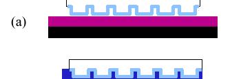
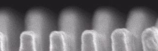
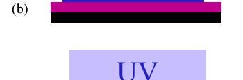
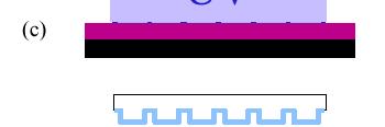
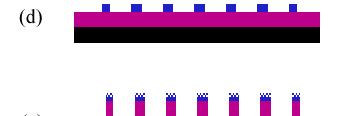
20 Nano-imprint Lithography Step&Flash Imprint Lithography 30 nm dense 20 nm isolated (G. Willson, UT Austin) Issues: Masks, Alignment, Inspection


21 Printing Over Topography is Possible MOS Device Two Layer Optical Element
22 Alignment
23 Mask Making e-beam writing (example Applied ETEC system) < 100 nm resolution, 15 5 nm grid 50 nm overlay (due to butting) very high cost ($50K/layer) optical writing (example ATEQ 4300) 180 nm resolution 25 nm overlay high cost ($20K/layer)
24 Status: Node by Node 2003: 90 nm node: Gates 65 nm Advanced semiconductor companies 90 nm Using 193 nm NA = 0854X 0.85 systems Lines => assist or phase-edges Contacts => multiple phase assist patterns Status 2006: 65 nm node: Gates 48 nm Use 193 nm NA = X systems Lines => assist or phase-edges edges Contacts: e-beam or multiple phase-assist Status nm node: Gates 32 nm Use 193 NA = 1.30 immersion with new liquid Lines =>Phase-edge Contacts: e-beam Or EUV 13.4 nm NA = 0.25
OPC Scatterbars or Assist Features
 OPC Scatterbars or Assist Features Main Feature The isolated main pattern now acts somewhat more like a periodic line and space pattern which has a higher quality image especially with focus when off-axis
Purpose: Explain the top advanced issues and concepts in
 Advanced Issues and Technology (AIT) Modules Purpose: Explain the top advanced issues and concepts in optical projection printing and electron-beam lithography. h AIT-1: LER and Chemically Amplified Resists
Update on 193nm immersion exposure tool
 Update on 193nm immersion exposure tool S. Owa, H. Nagasaka, Y. Ishii Nikon Corporation O. Hirakawa and T. Yamamoto Tokyo Electron Kyushu Ltd. January 28, 2004 Litho Forum 1 What is immersion lithography?
Purpose: Explain the top 10 phenomena and concepts. BPP-1: Resolution and Depth of Focus (1.5X)
") Basic Projection Printing (BPP) Modules Purpose: Explain the top 10 phenomena and concepts key to understanding optical projection printing BPP-1: Resolution and Depth of Focus (1.5X) BPP-2: Bragg condition
Basic Projection Printing (BPP) Modules Purpose: Explain the top 10 phenomena and concepts key to understanding optical projection printing BPP-1: Resolution and Depth of Focus (1.5X) BPP-2: Bragg condition
Optical Projection Printing and Modeling
 Optical Projection Printing and Modeling Overview of optical lithography, concepts, trends Basic Parameters and Effects (1-14) Resolution Depth of Focus; Proximity, MEEF, LES Image Calculation, Characterization
Optical Lithography. Here Is Why. Burn J. Lin SPIE PRESS. Bellingham, Washington USA
 Optical Lithography Here Is Why Burn J. Lin SPIE PRESS Bellingham, Washington USA Contents Preface xiii Chapter 1 Introducing Optical Lithography /1 1.1 The Role of Lithography in Integrated Circuit Fabrication
Challenges of EUV masks and preliminary evaluation
 Challenges of EUV masks and preliminary evaluation Naoya Hayashi Electronic Device Laboratory Dai Nippon Printing Co.,Ltd. EUV Mask Workshop 2004 1 Contents Recent Lithography Options on Roadmap Challenges
Mirror-based pattern generation for maskless lithography
 Microelectronic Engineering 73 74 (2004) 42 47 www.elsevier.com/locate/mee Mirror-based pattern generation for maskless lithography William G. Oldham *, Yashesh Shroff EECS Department, University of California,
Optical Maskless Lithography - OML
 Optical Maskless Lithography - OML Kevin Cummings 1, Arno Bleeker 1, Jorge Freyer 2, Jason Hintersteiner 1, Karel van der Mast 1, Tor Sandstrom 2 and Kars Troost 1 2 1 slide 1 Outline Why should you consider
Eun-Jin Kim, GukJin Kim, Seong-Sue Kim*, Han-Ku Cho*, Jinho Ahn**, Ilsin An, and Hye-Keun Oh
 Eun-Jin Kim, GukJin Kim, Seong-Sue Kim*, Han-Ku Cho*, Jinho Ahn**, Ilsin An, and Hye-Keun Oh Lithography Lab. Department of Applied Physics, Hanyang University, Korea *Samsung Electronics Co., LTD. Korea
From ArF Immersion to EUV Lithography
 From ArF Immersion to EUV Lithography Luc Van den hove Vice President IMEC Outline Introduction 193nm immersion lithography EUV lithography Global collaboration Conclusions Lithography is enabling 1000
Section 2: Lithography. Jaeger Chapter 2. EE143 Ali Javey Slide 5-1
 Section 2: Lithography Jaeger Chapter 2 EE143 Ali Javey Slide 5-1 The lithographic process EE143 Ali Javey Slide 5-2 Photolithographic Process (a) (b) (c) (d) (e) (f) (g) Substrate covered with silicon
5. Lithography. 1. photolithography intro: overall, clean room 2. principle 3. tools 4. pattern transfer 5. resolution 6. next-gen
 5. Lithography 1. photolithography intro: overall, clean room 2. principle 3. tools 4. pattern transfer 5. resolution 6. next-gen References: Semiconductor Devices: Physics and Technology. 2 nd Ed. SM
What s So Hard About Lithography?
 What s So Hard About Lithography? Chris A. Mack, www.lithoguru.com, Austin, Texas Optical lithography has been the mainstay of semiconductor patterning since the early days of integrated circuit production.
Comparative Study of Binary Intensity Mask and Attenuated Phase Shift Mask using Hyper-NA Immersion Lithography for Sub-45nm Era
 Comparative Study of Binary Intensity Mask and Attenuated Phase Shift Mask using Hyper-NA Immersion Lithogr for Sub-45nm Era Tae-Seung Eom*, Jun-Taek Park, Sarohan Park, Sunyoung Koo, Jin-Soo Kim, Byoung-Hoon
Optical Microlithography XXVIII
 PROCEEDINGS OF SPIE Optical Microlithography XXVIII Kafai Lai Andreas Erdmann Editors 24-26 February 2015 San Jose, California, United States Sponsored by SPIE Cosponsored by Cymer, an ASML company (United
Feature-level Compensation & Control
 Feature-level Compensation & Control 2 Lithography Andrew Neureuther and Costas Spanos, UCB Workshop & Review 04/15/2004 11/19/2003 - Lithography 3 Lithography: Andy Neureuther, UCB Research Themes: Linking
Tutor43.doc; Version 8/15/03 T h e L i t h o g r a p h y E x p e r t (November 2003)
") Tutor43.doc; Version /15/03 T h e L i t h o g r a p h y E x p e r t (November 2003) Scattering Bars Chris A. Mack, KLA-Tencor, FINLE Division, Austin, Texas Resolution enhancement technologies refer to
Tutor43.doc; Version /15/03 T h e L i t h o g r a p h y E x p e r t (November 2003) Scattering Bars Chris A. Mack, KLA-Tencor, FINLE Division, Austin, Texas Resolution enhancement technologies refer to
Copyright 2000, Society of Photo-Optical Instrumentation Engineers This paper was published in Optical Microlithography XIII, Volume 4000 and is made
 Copyright 00, Society of Photo-Optical Instrumentation Engineers This paper was published in Optical Microlithography XIII, Volume 4000 and is made available as an electronic reprint with permission of
Lithography. 3 rd. lecture: introduction. Prof. Yosi Shacham-Diamand. Fall 2004
 Lithography 3 rd lecture: introduction Prof. Yosi Shacham-Diamand Fall 2004 1 List of content Fundamental principles Characteristics parameters Exposure systems 2 Fundamental principles Aerial Image Exposure
Solid Immersion and Evanescent Wave Lithography at Numerical Apertures > 1.60
 Solid Immersion and Evanescent Wave Lithography at Numerical Apertures > 1.60 Bruce Smith Y. Fan, J. Zhou, L. Zavyalova, M. Slocum, J. Park, A. Bourov, E. Piscani, N. Lafferty, A. Estroff Rochester Institute
Discovering Electrical & Computer Engineering. Carmen S. Menoni Professor Week 3 armain.
 Discovering Electrical & Computer Engineering Carmen S. Menoni Professor Week 3 http://www.engr.colostate.edu/ece103/semin armain.html TOP TECH 2012 SPECIAL REPORT IEEE SPECTRUM PAGE 28, JANUARY 2012 P.E.
2009 International Workshop on EUV Lithography
 Contents Introduction Absorber Stack Optimization Non-flatness Correction Blank Defect and Its Mitigation Wafer Printing Inspection Actinic Metrology Cleaning and Repair Status Remaining Issues in EUV
Holistic View of Lithography for Double Patterning. Skip Miller ASML
 Holistic View of Lithography for Double Patterning Skip Miller ASML Outline Lithography Requirements ASML Holistic Lithography Solutions Conclusions Slide 2 Shrink Continues Lithography keeps adding value
Optical Lithography. Keeho Kim Nano Team / R&D DongbuAnam Semi
 Optical Lithography Keeho Kim Nano Team / R&D DongbuAnam Semi Contents Lithography = Photolithography = Optical Lithography CD : Critical Dimension Resist Pattern after Development Exposure Contents Optical
Micro- and Nano-Technology... for Optics
 Micro- and Nano-Technology...... for Optics 3.2 Lithography U.D. Zeitner Fraunhofer Institut für Angewandte Optik und Feinmechanik Jena Printing on Stones Map of Munich Stone Print Contact Printing light
ECSE 6300 IC Fabrication Laboratory Lecture 3 Photolithography. Lecture Outline
 ECSE 6300 IC Fabrication Laboratory Lecture 3 Photolithography Prof. James J. Q. Lu Bldg. CII, Rooms 6229 Rensselaer Polytechnic Institute Troy, NY 12180 Tel. (518)276 2909 e mails: luj@rpi.edu http://www.ecse.rpi.edu/courses/s18/ecse
Advanced Patterning Techniques for 22nm HP and beyond
 Advanced Patterning Techniques for 22nm HP and beyond An Overview IEEE LEOS (Bay Area) Yashesh A. Shroff Intel Corporation Aug 4 th, 2009 Outline The Challenge Advanced (optical) lithography overview Flavors
Mask Technology Development in Extreme-Ultraviolet Lithography
 Mask Technology Development in Extreme-Ultraviolet Lithography Anthony Yen September 6, 2013 Projected End of Optical Lithography 2013 TSMC, Ltd 1976 1979 1982 1985 1988 1991 1994 1997 2000 2003 2007 2012
Photolithography II ( Part 2 )
") 1 Photolithography II ( Part 2 ) Chapter 14 : Semiconductor Manufacturing Technology by M. Quirk & J. Serda Saroj Kumar Patra, Department of Electronics and Telecommunication, Norwegian University of Science
1 Photolithography II ( Part 2 ) Chapter 14 : Semiconductor Manufacturing Technology by M. Quirk & J. Serda Saroj Kumar Patra, Department of Electronics and Telecommunication, Norwegian University of Science
Optics for EUV Lithography
 Optics for EUV Lithography Dr. Sascha Migura, Carl Zeiss SMT GmbH, Oberkochen, Germany 2018 EUVL Workshop June 13 th, 2018 Berkeley, CA, USA The resolution of the optical system determines the minimum
Photolithography. References: Introduction to Microlithography Thompson, Willson & Bowder, 1994
 Photolithography References: Introduction to Microlithography Thompson, Willson & Bowder, 1994 Microlithography, Science and Technology Sheats & Smith, 1998 Any other Microlithography or Photolithography
Lecture 5. Optical Lithography
 Lecture 5 Optical Lithography Intro For most of microfabrication purposes the process (e.g. additive, subtractive or implantation) has to be applied selectively to particular areas of the wafer: patterning
IMEC update. A.M. Goethals. IMEC, Leuven, Belgium
 IMEC update A.M. Goethals IMEC, Leuven, Belgium Outline IMEC litho program overview ASML ADT status 1 st imaging Tool description Resist projects Screening using interference litho K LUP / Novel resist
Synthesis of projection lithography for low k1 via interferometry
 Synthesis of projection lithography for low k1 via interferometry Frank Cropanese *, Anatoly Bourov, Yongfa Fan, Andrew Estroff, Lena Zavyalova, Bruce W. Smith Center for Nanolithography Research, Rochester
Section 2: Lithography. Jaeger Chapter 2 Litho Reader. EE143 Ali Javey Slide 5-1
 Section 2: Lithography Jaeger Chapter 2 Litho Reader EE143 Ali Javey Slide 5-1 The lithographic process EE143 Ali Javey Slide 5-2 Photolithographic Process (a) (b) (c) (d) (e) (f) (g) Substrate covered
The future of EUVL. Outline. by Winfried Kaiser, Udo Dinger, Peter Kuerz, Martin Lowisch, Hans-Juergen Mann, Stefan Muellender,
 The future of EUVL by Winfried Kaiser, Udo Dinger, Peter Kuerz, Martin Lowisch, Hans-Juergen Mann, Stefan Muellender, William H. Arnold, Jos Benshop, Steven G. Hansen, Koen van Ingen-Schenau Outline Introduction
EE143 Fall 2016 Microfabrication Technologies. Lecture 3: Lithography Reading: Jaeger, Chap. 2
 EE143 Fall 2016 Microfabrication Technologies Lecture 3: Lithography Reading: Jaeger, Chap. 2 Prof. Ming C. Wu wu@eecs.berkeley.edu 511 Sutardja Dai Hall (SDH) 1-1 The lithographic process 1-2 1 Photolithographic
Lecture 7. Lithography and Pattern Transfer. Reading: Chapter 7
 Lecture 7 Lithography and Pattern Transfer Reading: Chapter 7 Used for Pattern transfer into oxides, metals, semiconductors. 3 types of Photoresists (PR): Lithography and Photoresists 1.) Positive: PR
OPTICAL LITHOGRAPHY INTO THE MILLENNIUM: SENSITIVITY TO ABERRATIONS, VIBRATION AND POLARIZATION
 OPTICAL LITHOGRAPHY INTO THE MILLENNIUM: SENSITIVITY TO ABERRATIONS, VIBRATION AND POLARIZATION Donis G. Flagello a, Jan Mulkens b, and Christian Wagner c a ASML, 8555 S. River Parkway, Tempe, AZ 858,
Section 2: Lithography. Jaeger Chapter 2 Litho Reader. The lithographic process
 Section 2: Lithography Jaeger Chapter 2 Litho Reader The lithographic process Photolithographic Process (a) (b) (c) (d) (e) (f) (g) Substrate covered with silicon dioxide barrier layer Positive photoresist
EE-527: MicroFabrication
 EE-57: MicroFabrication Exposure and Imaging Photons white light Hg arc lamp filtered Hg arc lamp excimer laser x-rays from synchrotron Electrons Ions Exposure Sources focused electron beam direct write
Polarization Experiments Using Jones Calculus
 Polarization Experiments Using Jones Calculus Reference http://chaos.swarthmore.edu/courses/physics50_2008/p50_optics/04_polariz_matrices.pdf Theory In Jones calculus, the polarization state of light is
TECHNOLOGY ROADMAP 2006 UPDATE LITHOGRAPHY FOR
 INTERNATIONAL TECHNOLOGY ROADMAP FOR SEMICONDUCTORS 2006 UPDATE LITHOGRAPHY THE ITRS IS DEVISED AND INTENDED FOR TECHNOLOGY ASSESSMENT ONLY AND IS WITHOUT REGARD TO ANY COMMERCIAL CONSIDERATIONS PERTAINING
Immersion Lithography: New Opportunities for Semiconductor Manufacturing
 Immersion Lithography: New Opportunities for Semiconductor Manufacturing Tim Brunner, Dario Gil, Carlos Fonseca and Nakgeuon Seong IBM - SRDC Bob Streefkerk, Christian Wagner and Marco Stavenga ASML Outline
Results of Proof-of-Concept 50keV electron multi-beam Mask Exposure Tool (emet POC)
") Results of Proof-of-Concept 50keV electron multi-beam Mask Exposure Tool (emet POC) Elmar Platzgummer *, Christof Klein, and Hans Loeschner IMS Nanofabrication AG Schreygasse 3, A-1020 Vienna, Austria
Results of Proof-of-Concept 50keV electron multi-beam Mask Exposure Tool (emet POC) Elmar Platzgummer *, Christof Klein, and Hans Loeschner IMS Nanofabrication AG Schreygasse 3, A-1020 Vienna, Austria
Major Fabrication Steps in MOS Process Flow
 Major Fabrication Steps in MOS Process Flow UV light Mask oxygen Silicon dioxide photoresist exposed photoresist oxide Silicon substrate Oxidation (Field oxide) Photoresist Coating Mask-Wafer Alignment
TSMC Property. EUV Lithography. The March toward HVM. Anthony Yen. 9 September TSMC, Ltd
 EUV Lithography The March toward HVM Anthony Yen 9 September 2016 1 1 st EUV lithography setup and results, 1986 Si Stencil Mask SR W/C Multilayer Coating Optics λ=11 nm, provided by synchrotron radiation
Impact of 3-D Mask Effects on CD and Overlay over Image Field in Extreme Ultraviolet Lithography
 Impact of 3-D Mask Effects on CD and Overlay over Image Field in Extreme Ultraviolet Lithography 5 th International EUV Symposium Barcelona, Spain Sven Trogisch Markus Bender Frank-Michael Kamm Disclaimer
EUVL getting ready for volume introduction
 EUVL getting ready for volume introduction SEMICON West 2010 Hans Meiling, July 14, 2010 Slide 1 public Outline ASML s Lithography roadmap to support Moore s Law Progress on 0.25NA EUV systems Progress
MICROCHIP MANUFACTURING by S. Wolf
 MICROCHIP MANUFACTURING by S. Wolf Chapter 19 LITHOGRAPHY II: IMAGE-FORMATION and OPTICAL HARDWARE 2004 by LATTICE PRESS CHAPTER 19 - CONTENTS Preliminaries: Wave- Motion & The Behavior of Light Resolution
The End of Thresholds: Subwavelength Optical Linewidth Measurement Using the Flux-Area Technique
 The End of Thresholds: Subwavelength Optical Linewidth Measurement Using the Flux-Area Technique Peter Fiekowsky Automated Visual Inspection, Los Altos, California ABSTRACT The patented Flux-Area technique
IMPACT Lithography/DfM Roundtable
 IMPACT Lithography/DfM Roundtable Focus Match Location Z 0 Neureuther Research Group Juliet Rubinstein, Eric Chin, Chris Clifford, Marshal Miller, Lynn Wang, Kenji Yamazoe Visiting Industrial Fellow, Canon,
UV Nanoimprint Stepper Technology: Status and Roadmap. S.V. Sreenivasan Sematech Litho Forum May 14 th, 2008
 UV Nanoimprint Stepper Technology: Status and Roadmap S.V. Sreenivasan Sematech Litho Forum May 14 th, 2008 Overview Introduction Stepper technology status: Patterning and CD Control Through Etch Alignment
Scope and Limit of Lithography to the End of Moore s Law
 Scope and Limit of Lithography to the End of Moore s Law Burn J. Lin tsmc, Inc. 1 What dictate the end of Moore s Law Economy Device limits Lithography limits 2 Litho Requirement of Critical Layers Logic
Part 5-1: Lithography
 Part 5-1: Lithography Yao-Joe Yang 1 Pattern Transfer (Patterning) Types of lithography systems: Optical X-ray electron beam writer (non-traditional, no masks) Two-dimensional pattern transfer: limited
Registration performance on EUV masks using high-resolution registration metrology
 Registration performance on EUV masks using high-resolution registration metrology Steffen Steinert a, Hans-Michael Solowan a, Jinback Park b, Hakseung Han b, Dirk Beyer a, Thomas Scherübl a a Carl Zeiss
 http://goldberg.lbl.gov 1 To EUV or not to EUV? That is the question. Do we need EUV interferometry and EUV optical testing? 17 Things you need to know about perfecting EUV optics. 2 The main things you
immersion optics Immersion Lithography with ASML HydroLith TWINSCAN System Modifications for Immersion Lithography by Bob Streefkerk
 immersion optics Immersion Lithography with ASML HydroLith by Bob Streefkerk For more than 25 years, many in the semiconductor industry have predicted the end of optical lithography. Recent developments,
EUV Lithography Transition from Research to Commercialization
 EUV Lithography Transition from Research to Commercialization Charles W. Gwyn and Peter J. Silverman and Intel Corporation Photomask Japan 2003 Pacifico Yokohama, Kanagawa, Japan Gwyn:PMJ:4/17/03:1 EUV
1X Broadband Wafer Stepper for Bump and Wafer Level Chip Scale Packaging (CSP) Applications
 Applications") 1X Broadband Wafer Stepper for Bump and Wafer Level Chip Scale Packaging (CSP) Applications Doug Anberg, Mitch Eguchi, Takahiro Momobayashi Ultratech Stepper, Inc. San Jose, California Takeshi Wakabayashi,
1X Broadband Wafer Stepper for Bump and Wafer Level Chip Scale Packaging (CSP) Applications Doug Anberg, Mitch Eguchi, Takahiro Momobayashi Ultratech Stepper, Inc. San Jose, California Takeshi Wakabayashi,
Computer Generated Holograms for Optical Testing
 Computer Generated Holograms for Optical Testing Dr. Jim Burge Associate Professor Optical Sciences and Astronomy University of Arizona jburge@optics.arizona.edu 520-621-8182 Computer Generated Holograms
Optical Maskless Lithography (OML) Project Status
 Project Status") Optical Maskless Lithography (OML) Project Status Timothy O Neil, Arno Bleeker, Kars Troost SEMATECH ML 2 Conference January 2005 / Slide 1 Agenda Introduction and Principles of Operation DARPA Program
Optical Maskless Lithography (OML) Project Status Timothy O Neil, Arno Bleeker, Kars Troost SEMATECH ML 2 Conference January 2005 / Slide 1 Agenda Introduction and Principles of Operation DARPA Program
Semiconductor Manufacturing Technology. Semiconductor Manufacturing Technology. Photolithography: Resist Development and Advanced Lithography
 Semiconductor Manufacturing Technology Michael Quirk & Julian Serda October 2001 by Prentice Hall Chapter 15 Photolithography: Resist Development and Advanced Lithography Eight Basic Steps of Photolithography
16nm with 193nm Immersion Lithography and Double Exposure
 16nm with 193nm Immersion Lithography and Double Exposure Valery Axelrad, Sequoia Design Systems, Inc. (United States) Michael C. Smayling, Tela Innovations, Inc. (United States) ABSTRACT Gridded Design
ADVANCED TECHNOLOGY FOR EXTENDING OPTICAL LITHOGRAPHY
 ADVANCED TECHNOLOGY FOR EXTENDING OPTICAL LITHOGRAPHY Christian Wagner a, Winfried Kaiser a, Jan Mulkens b, Donis G. Flagello c a Carl Zeiss, D-73446 Oberkochen, Germany; b ASM Lithography, De Run 1110,
State-of-the-art device fabrication techniques
 State-of-the-art device fabrication techniques! Standard Photo-lithography and e-beam lithography! Advanced lithography techniques used in semiconductor industry Deposition: Thermal evaporation, e-gun
Copyright 2002 by the Society of Photo-Optical Instrumentation Engineers.
 Copyright 22 by the Society of Photo-Optical Instrumentation Engineers. This paper was published in the proceedings of Optical Microlithography XV, SPIE Vol. 4691, pp. 98-16. It is made available as an
Lithography Roadmap. without immersion lithography. Node Half pitch. 248nm. 193nm. 157nm EUVL. 3-year cycle: 2-year cycle: imec 2005
 Lithography Roadmap without immersion lithography Node Half pitch 180 nm 130 nm 90 nm 65 nm 45 nm 32 nm 22 nm 250 nm 180 nm 130 nm 90 nm 65 nm 45 nm 32 nm 248nm 193nm 157nm EUVL 3-year cycle: 2-year cycle:
Progress in full field EUV lithography program at IMEC
 Progress in full field EUV lithography program at IMEC A.M. Goethals*, G.F. Lorusso*, R. Jonckheere*, B. Baudemprez*, J. Hermans*, F. Iwamoto 1, B.S. Kim 2, I.S. Kim 2, A. Myers 3, A. Niroomand 4, N. Stepanenko
Institute of Solid State Physics. Technische Universität Graz. Lithography. Peter Hadley
 Technische Universität Graz Institute of Solid State Physics Lithography Peter Hadley http://www.cleanroom.byu.edu/virtual_cleanroom.parts/lithography.html http://www.cleanroom.byu.edu/su8.phtml Spin coater
Light Sources for EUV Mask Metrology. Heiko Feldmann, Ulrich Müller
 Light Sources for EUV Mask Metrology Heiko Feldmann, Ulrich Müller Dublin, October 9, 2012 Agenda 1 2 3 4 Actinic Metrology in Mask Making The AIMS EUV Concept Metrology Performance Drivers and their Relation
MICRO AND NANOPROCESSING TECHNOLOGIES
 MICRO AND NANOPROCESSING TECHNOLOGIES LECTURE 4 Optical lithography Concepts and processes Lithography systems Fundamental limitations and other issues Photoresists Photolithography process Process parameter
Lithography Simulation Tools Needed for 22nm HP and Beyond. Chris Mack
 Lithography Simulation Tools Needed for 22nm HP and Beyond Chris Mack www.lithoguru.com Slicing the Pie Simulation Tool Characteristics Precision Accuracy Capabilities (speed, features) Simulation Tool
Will contain image distance after raytrace Will contain image height after raytrace
 Name: LASR 51 Final Exam May 29, 2002 Answer all questions. Module numbers are for guidance, some material is from class handouts. Exam ends at 8:20 pm. Ynu Raytracing The first questions refer to the
Copyright 2004 by the Society of Photo-Optical Instrumentation Engineers.
 Copyright 2004 by the Society of Photo-Optical Instrumentation Engineers. This paper was published in the proceedings of Emerging Lithographic Technologies VIII, SPIE Vol. 5374, pp. 1-8. It is made available
Process Optimization
 Process Optimization Process Flow for non-critical layer optimization START Find the swing curve for the desired resist thickness. Determine the resist thickness (spin speed) from the swing curve and find
Shot noise and process window study for printing small contacts using EUVL. Sang Hun Lee John Bjorkohlm Robert Bristol
 Shot noise and process window study for printing small contacts using EUVL Sang Hun Lee John Bjorkohlm Robert Bristol Abstract There are two issues in printing small contacts with EUV lithography (EUVL).
Electron Multi-Beam Technology for Mask and Wafer Direct Write. Elmar Platzgummer IMS Nanofabrication AG
 Electron Multi-Beam Technology for Mask and Wafer Direct Write Elmar Platzgummer IMS Nanofabrication AG Contents 2 Motivation for Multi-Beam Mask Writer (MBMW) MBMW Tool Principles and Architecture MBMW
Performance data of a new 248 nm CD metrology tool proved on COG reticles and PSM s
 Performance data of a new 248 nm CD metrology tool proved on COG reticles and PSM s Gerhard Schlueter a, Walter Steinberg a, John Whittey b a Leica Microsystems Wetzlar GmbH Ernst-Leitz-Str. 17-37, D-35578
Newer process technology (since 1999) includes :
 includes :") Newer process technology (since 1999) includes : copper metalization hi-k dielectrics for gate insulators si on insulator strained silicon lo-k dielectrics for interconnects Immersion lithography for masks
Newer process technology (since 1999) includes : copper metalization hi-k dielectrics for gate insulators si on insulator strained silicon lo-k dielectrics for interconnects Immersion lithography for masks
Feature-level Compensation & Control
 Feature-level Compensation & Control 2 Lithography Andy Neureuther and Costas Spanos, UCB Workshop 11/19/2003 11/19/2003 - Lithography 3 Lithography: Andy Neureuther, UCB Research Themes: Blowing the horn
(Complementary E-Beam Lithography)
") Extending Optical Lithography with C E B L (Complementary E-Beam Lithography) July 13, 2011 4008 Burton Drive, Santa Clara, CA 95054 Outline Complementary Lithography E-Beam Complements Optical Multibeam
Extending Optical Lithography with C E B L (Complementary E-Beam Lithography) July 13, 2011 4008 Burton Drive, Santa Clara, CA 95054 Outline Complementary Lithography E-Beam Complements Optical Multibeam
EUVL Activities in China. Xiangzhao Wang Shanghai Inst. Of Opt. and Fine Mech. Of CAS. (SIOM) Shanghai, China.
 Shanghai, China.") EUVL Activities in China Xiangzhao Wang Shanghai Inst. Of Opt. and Fine Mech. Of CAS. (SIOM) Shanghai, China. wxz26267@siom.ac.cn Projection Optics Imaging System Surface Testing Optical Machining ML Coating
EUVL Activities in China Xiangzhao Wang Shanghai Inst. Of Opt. and Fine Mech. Of CAS. (SIOM) Shanghai, China. wxz26267@siom.ac.cn Projection Optics Imaging System Surface Testing Optical Machining ML Coating
2008 European EUVL. EUV activities the EUVL shop future plans. Rob Hartman
 2008 European EUVL EUV activities the EUVL shop future plans Rob Hartman 2007 international EUVL Symposium 28-31 October 2007 2008 international EUVL Symposium 28 Sapporo, September Japan 1 October 2008
INTERNATIONAL TECHNOLOGY ROADMAP SEMICONDUCTORS 2001 EDITION LITHOGRAPHY FOR
 INTERNATIONAL TECHNOLOGY ROADMAP FOR SEMICONDUCTORS 2001 EDITION LITHOGRAPHY TABLE OF CONTENTS Scope...1 Difficult Challenges...1 Lithography Technology Requirements...3 Potential Solutions...14 Crosscut
Reducing Proximity Effects in Optical Lithography
 INTERFACE '96 This paper was published in the proceedings of the Olin Microlithography Seminar, Interface '96, pp. 325-336. It is made available as an electronic reprint with permission of Olin Microelectronic
Optical Proximity Effects
 T h e L i t h o g r a p h y E x p e r t (Spring 1996) Optical Proximity Effects Chris A. Mack, FINLE Technologies, Austin, Texas Proximity effects are the variations in the linewidth of a feature (or the
Scaling of Semiconductor Integrated Circuits and EUV Lithography
 Scaling of Semiconductor Integrated Circuits and EUV Lithography ( 半導体集積回路の微細化と EUV リソグラフィー ) December 13, 2016 EIDEC (Emerging nano process Infrastructure Development Center, Inc.) Hidemi Ishiuchi 1 OUTLINE
Electron Beam Lithography. Adam Ramm
 Electron Beam Lithography Adam Ramm Why use electrons? Negligible diffraction limitations: R = k λ NA With current optical technology, this equates to about 45nm resolution. For an electron, wavelength
Akira Miyake, Chidane Ouchi, International EUVL Symposium, October , Kobe Slide 1
 Development Status of Canon s EUVL Exposure Tool Akira Miyake, Chidane Ouchi, Hideki Morishima, and Hiroyoshi Kubo Canon Inc. International EUVL Symposium, October 18 2010, Kobe Slide 1 Outline EUVL Exposure
Outline. 1 Introduction. 2 Basic IC fabrication processes. 3 Fabrication techniques for MEMS. 4 Applications. 5 Mechanics issues on MEMS MDL NTHU
 Outline 1 Introduction 2 Basic IC fabrication processes 3 Fabrication techniques for MEMS 4 Applications 5 Mechanics issues on MEMS 2.2 Lithography Reading: Runyan Chap. 5, or 莊達人 Chap. 7, or Wolf and
Micro- and Nano-Technology... for Optics
 Micro- and Nano-Technology...... for Optics 3.2 Lithography U.D. Zeitner Fraunhofer Institut für Angewandte Optik und Feinmechanik Jena Printing on Stones Map of Munich Stone Print Shadow Printing Photomask
Approaching the NA of Water: Immersion Lithography at 193nm
 Approaching the NA of Water: Immersion Lithography at 193nm Bruce Smith Y. Fan, A. Bourov, L. Zavyalova, J. Zhou, F. Cropanese, N. Lafferty Rochester Institute of Technology M. Gower, D. Ashworth Exitech
Lithography on the Edge
 Lithography on the Edge David Medeiros IBM Prague, Czech Republic 3 October 009 An Edge A line where an something begins or ends: A border, a discontinuity, a threshold Scaling Trend End of an Era? 0000
Computational Lithography
 Computational Lithography An EDA Perspective Frank Schellenberg, Ph.D. Mentor Graphics 22nm SEMATECH Workshop 5/15/2008 22nm Optical Lithography 22nm with λ = 193nm Wow! Several processing options Double
Optolith 2D Lithography Simulator
 2D Lithography Simulator Advanced 2D Optical Lithography Simulator 4/13/05 Introduction is a powerful non-planar 2D lithography simulator that models all aspects of modern deep sub-micron lithography It
Topography effects and wave aberrations in advanced PSM-technology
 Header for SPIE use Topography effects and wave aberrations in advanced PSM-technology Andreas Erdmann Fraunhofer Institute of Integrated Circuits, Device Technology Division (IIS-B), Schottkystrasse 1,
Imec pushes the limits of EUV lithography single exposure for future logic and memory
 Edition March 2018 Semiconductor technology & processing Imec pushes the limits of EUV lithography single exposure for future logic and memory Imec has made considerable progress towards enabling extreme
TECHNOLOGY ROADMAP 2005 EDITION LITHOGRAPHY FOR
 INTERNATIONAL TECHNOLOGY ROADMAP FOR SEMICONDUCTORS 2005 EDITION LITHOGRAPHY THE ITRS IS DEVISED AND INTENDED FOR TECHNOLOGY ASSESSMENT ONLY AND IS WITHOUT REGARD TO ANY COMMERCIAL CONSIDERATIONS PERTAINING