Purpose: Explain the top advanced issues and concepts in
|
|
|
- Blaise Patrick
- 6 years ago
- Views:
Transcription
1 Advanced Issues and Technology (AIT) Modules Purpose: Explain the top advanced issues and concepts in optical projection printing and electron-beam lithography. h AIT-1: LER and Chemically Amplified Resists * AIT-2: Resolution Enhancement and PSM AIT-3: Small Features and Defects AIT-4: Aberrations AIT-5: Maskless, High-NA, Immersion, EUV, Imprint Each module is a min presentation of about a dozen slides. Suggested reading: Griffin: Plummer, Deal and Chapter 5 Sheats and Smith: , Wong: 34-37, 71-90, Fig 4.1, Fig. 4.10,
2 OPC Scatterbars or Assist Features Main Feature The isolated main pattern now acts somewhat more like a periodic line and space pattern which has a higher quality image especially with focus when off-axis illumination is used. The bars must be small enough that the image at their location does not print. Add nonprinting adjacent features A typical size is about 1/3 of the minimum feature size and they are placed about a minimum feature size from the feature edge.
3 Scattering Bar Simulation with TEMPEST λ=193nm Mag=4X CD Incident radiation target =130nm SB CD E y TE : E y polarization z-axis y-axis μm Image CD x-axis With SB E x μm TM : E x polarization Aerial Scatterbars improve DOF Defocus μm μm Adam, SPIE
4 Scattering Bar Aerial Image and Design λ=193nm, NA=0.7, σ=0.6, Mag=4X, CD target =130nm Norm malized Inten nsity Aerial Image (Best focus) SPLAT TE TM Intensity Intensity dip of SB SPLAT TE TM Perturbation model (μm) Size of SB (λ/na) - Observe that the scatter bars (also the main feature) appear wider in TM (field perpendicular) excitation than in TE (field parallel) and narrower with SPLAT simulation (scalar theory) Adam, SPIE
5 OPC Feature Design Data: Binary Masks TEMPEST-CF vs. SPLAT-CF differ by 9% TEMPEST-DF vs. SPLAT-DF differ by 6% Perturbation is proportional to OPC area. in nm 1/2 (LE ES corre ection) 1/2 Wave propagation and polarization are 2 nd order for binary masks. CF = Clear Field DF = Dark Field TEMPEST-CF Line end shortening (LES) correction SPLAT-CF SPLAT-DF TEMPEST-DF equiv. size of OPC in l/na (1X) Adam, SPIE Serif
6 High-Fidelity Audio System Off-Axis Analogy The lateral spatial variation across a wafer of an off-axis light ray is analogous the temporal variation of a note in a Hi-Fi audio system. More rapid variations (spatial or temporal) from higher frequencies (spatial or temporal) allow sharper artifacts t (spatial {lithography feature} or temporal {drum beat}) to be produced. Just as it is difficult to improve upon the pulse width times bandwidth product it is difficult to improve upon the feature size times NA product. BUT IN RESOLUTION ENHANCEMENT WE TRY TO GET A FACTOR OF TWO INCREASE ANYWAY.
7 Resolution Enhancement Techniques Resolution Enhancement Emphasizes High Frequencies Conventional Illumination Binary Mask Modified Illumination 0 Frequency 0 Frequency Phase Mask Lens Capture 0 0 Frequency Frequency 0 0 Frequency In-Lens Filter Frequency Bokor, Neureuther, Oldham, Circuits and Devices, 1996
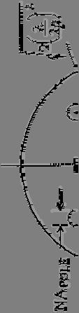
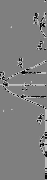
8 Two Ray Infinite DOF Ray # 1 θ 1 θ 2 k y Ray # 2 k x Pitch When θ 1 =θθ 2 the contributions from Ray #1 and Ray #2 track each exactly with axial distance and an INFINITE depth of focus is produced. Period = Pitch = Δk Transverse = = λ 2sin θ 2k 0 Δ 2π k Transverse sin( θ ) sin( θ ) = NA λ ( θ ) 2 NA Doubled Resolution! With infinite DOF
9 Strategy to improve both resolution and DOF Since the small features or edges are are most important emphasize the high-frequency off-axis ray to improve resolution. σ SPOT = λ Pitch NA Since the change in the image with focus comes from the relative phase change among the rays with axial distance, utilize rays at similar azimuthal angles that track in phase with focus to improve DOF.
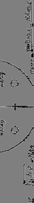
10 Top Hat General Shapes Illumination Schemes Annular DOF, Contacts k 1 = 0.67 k 1 = 0.55 σ k = 1.3 k = 1.7 IN = σ OUT = 0.85 Pupil Pupil Quadruple H,V lines, DOF k 1 = 0.45 k 2 = 2.0 Dipole V lines, DOF k 1 = 0.35 k 2 = Pupil Pupil The k1 factor is inversely proportional to the lateral separation of the illumination k 1 = 1/(2 x separation) H lines and contacts formed via a double exposure


11 Annular Illumination: k 1 =0.4 Large DOF L = S = 0.4 σ IN = 0.5 σ OUT = 0.8 DOF = 2.0 Contrast = 0.61
12 Quadrapole Illumination 0.4 l/na Line equal Space (Dense) DOF =1 σ x =σ y =0.6 σ POLE = 0.1 Higher contrast than annular for Manhattan geometries as there are no illumination components near either σ x =0 or σ y = 0


13 Quadrapole Optimization Dipole illumination i i can print smaller lines but lines only.
14 Phase-Shifting Mask Types Alternating (Strong) Attenuating (Weak) Used for Contacts 6% to 10% gives slope improvement of 30%. Sidelobe issue. Phase Edge Requires second trim mask exposure. Chromeless (Only 0 order)


15 Attenuating Phase-Shifting Masks Intensity of 6% comes from an electric field of Going from positive electric fields to negative electric fields increases edge slope and creates darker intensity near edge.

16 Phase-Shifting Mask P P Perfect Null P P/2 Frequency doubled Sheats and Smith


17 Phase-Shifting Mask: Electric Fields Sheats and Smith
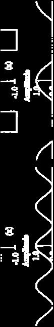
18 Alternating Phase-Shifting Mask 0.7 Alternating 0 and 180 regions, σ = 0.3 In Focus 1 RU Defocus The period on the wafer is ½ the period of the mask. The region < 0.3 intensity is about 1/3 of the period.
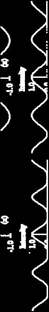
19 Phase-Edge (Perfect Null) 1.5 λ/na 0 and 180 regions, σ = 0.3 In Focus RU Defocus The width is about 0.3λ/NA. Great depth of focus.


20 Phase-Edge Masks Is trim or conjugate shifter better?
21 Focus Monitor 1.5 l/na 0 and 90 regions with 0.4 λ/na chrome, σ = 0.3 In Focus 1 RU Defocus 0 Cr 90 0 Cr 90 The shift is nearly linear with focus.
22 Phase-Edge Simulation in SPLAT 1.5 λ/na 0 and 180 regions, σ = 0.3 In Focus SPLAT INPUT FILE # Phase Edge DOF=0.0 2: 0.5 3: 0.5 4: 0.0 5: : : at 1.0 7: at 1.0 <180.0> 10:; 14: 'twolines.txt' 0:end; Implicit Symmetry for statement 7
23 Appropriate RETs for Various Patterns pˆ is the mask period in λ/na From Wong, RET in OL.
24 TEMPEST Instantaneous Electric Fields


25 Alt-PSM Intensity Imbalance: Edge Effects Δ IEDM, 1992 Wong
26 Photomask Polarization Effects When openings reach the size of 2 wavelengths polarization effects occur and they also are somewhat worse with off-axis illumination. However, for binary masks they are mitigated by the fact that the chrome is only about 80nm thick. The attached data shows that at λ = 193 nm and 80 nm of chrome the effects are probably not measurable for 1.5λ (300nm) openings. For 1.0λ (200nm) openings the desired TE polarization is favored by a factor of 1.2 for both the 0 th and 1 st orders.
27 Order Magnitudes: FDTD (Normalized) 0 th Order Magnitude Cr = 80nm Zeroth Order Magnitude (cr = 193 nm Lambda) Normalized λ TE Polarization TM Polarization Mask Pitch (4x) (um) Magnitude Cr = 200nm Zeroth Order Magnitude (cr = nm Lambda) TE Polarization 0.1 λ TM Polarization Mask Pitch (4x) (um ) 1st Order Magn nitude First Order Magnitude (cr = 193nm Lambda) Normalized λ TE Polarization TM Polarization Mask Pitch (4x) (um) agnitude Ma First Order Magnitude (cr = 193 nm Lambda) Normalized TE Polarization 0.1 TM Polarization 0.05 λ Mask Pitch (4x) (um) Data from Neureuther, Sematech 2003 Situation is worse for Attenuated masks due to their thickness, Progler, SPIE 05


28 Resolution Enhancement: In-Lens Filter cos ( ) j2πβ r j2πβ r 2πβr = 0.5e + 0.5e Defocus away and toward the lens. The cos(2πβr 2 ) filter creates dual defocused images that are very effective in increasing the total focal range of contact patterns. Fukuda Fukuda, JVST B Hitachi Nov/Dec 91
OPC Scatterbars or Assist Features
 OPC Scatterbars or Assist Features Main Feature The isolated main pattern now acts somewhat more like a periodic line and space pattern which has a higher quality image especially with focus when off-axis
Purpose: Explain the top 10 phenomena and concepts. BPP-1: Resolution and Depth of Focus (1.5X)
") Basic Projection Printing (BPP) Modules Purpose: Explain the top 10 phenomena and concepts key to understanding optical projection printing BPP-1: Resolution and Depth of Focus (1.5X) BPP-2: Bragg condition
Basic Projection Printing (BPP) Modules Purpose: Explain the top 10 phenomena and concepts key to understanding optical projection printing BPP-1: Resolution and Depth of Focus (1.5X) BPP-2: Bragg condition
Optical Projection Printing and Modeling
 Optical Projection Printing and Modeling Overview of optical lithography, concepts, trends Basic Parameters and Effects (1-14) Resolution Depth of Focus; Proximity, MEEF, LES Image Calculation, Characterization
* AIT-5: Maskless, High-NA, Immersion, EUV, Imprint
 Advanced Issues and Technology (AIT) Modules Purpose: Explain the top advanced issues and concepts in optical projection printing and electron-beam lithography. AIT-1: LER and CAR AIT-2: Resolution Enhancement
Mutually Optimizing Resolution Enhancement Techniques: Illumination, APSM, Assist Feature OPC, and Gray Bars
 Mutually Optimizing Resolution Enhancement Techniques: Illumination, APSM, Assist Feature OPC, and Gray Bars Bruce W. Smith Rochester Institute of Technology, Microelectronic Engineering Department, 82
Copyright 2000, Society of Photo-Optical Instrumentation Engineers This paper was published in Optical Microlithography XIII, Volume 4000 and is made
 Copyright 00, Society of Photo-Optical Instrumentation Engineers This paper was published in Optical Microlithography XIII, Volume 4000 and is made available as an electronic reprint with permission of
Update on 193nm immersion exposure tool
 Update on 193nm immersion exposure tool S. Owa, H. Nagasaka, Y. Ishii Nikon Corporation O. Hirakawa and T. Yamamoto Tokyo Electron Kyushu Ltd. January 28, 2004 Litho Forum 1 What is immersion lithography?
Optical Lithography. Keeho Kim Nano Team / R&D DongbuAnam Semi
 Optical Lithography Keeho Kim Nano Team / R&D DongbuAnam Semi Contents Lithography = Photolithography = Optical Lithography CD : Critical Dimension Resist Pattern after Development Exposure Contents Optical
The Formation of an Aerial Image, part 3
 T h e L i t h o g r a p h y T u t o r (July 1993) The Formation of an Aerial Image, part 3 Chris A. Mack, FINLE Technologies, Austin, Texas In the last two issues, we described how a projection system
Comparative Study of Binary Intensity Mask and Attenuated Phase Shift Mask using Hyper-NA Immersion Lithography for Sub-45nm Era
 Comparative Study of Binary Intensity Mask and Attenuated Phase Shift Mask using Hyper-NA Immersion Lithogr for Sub-45nm Era Tae-Seung Eom*, Jun-Taek Park, Sarohan Park, Sunyoung Koo, Jin-Soo Kim, Byoung-Hoon
Synthesis of projection lithography for low k1 via interferometry
 Synthesis of projection lithography for low k1 via interferometry Frank Cropanese *, Anatoly Bourov, Yongfa Fan, Andrew Estroff, Lena Zavyalova, Bruce W. Smith Center for Nanolithography Research, Rochester
Feature-level Compensation & Control
 Feature-level Compensation & Control 2 Lithography Andrew Neureuther and Costas Spanos, UCB Workshop & Review 04/15/2004 11/19/2003 - Lithography 3 Lithography: Andy Neureuther, UCB Research Themes: Linking
Section 2: Lithography. Jaeger Chapter 2. EE143 Ali Javey Slide 5-1
 Section 2: Lithography Jaeger Chapter 2 EE143 Ali Javey Slide 5-1 The lithographic process EE143 Ali Javey Slide 5-2 Photolithographic Process (a) (b) (c) (d) (e) (f) (g) Substrate covered with silicon
The Formation of an Aerial Image, part 2
 T h e L i t h o g r a p h y T u t o r (April 1993) The Formation of an Aerial Image, part 2 Chris A. Mack, FINLE Technologies, Austin, Texas In the last issue, we began to described how a projection system
Tutor43.doc; Version 8/15/03 T h e L i t h o g r a p h y E x p e r t (November 2003)
") Tutor43.doc; Version /15/03 T h e L i t h o g r a p h y E x p e r t (November 2003) Scattering Bars Chris A. Mack, KLA-Tencor, FINLE Division, Austin, Texas Resolution enhancement technologies refer to
Tutor43.doc; Version /15/03 T h e L i t h o g r a p h y E x p e r t (November 2003) Scattering Bars Chris A. Mack, KLA-Tencor, FINLE Division, Austin, Texas Resolution enhancement technologies refer to
Mirror-based pattern generation for maskless lithography
 Microelectronic Engineering 73 74 (2004) 42 47 www.elsevier.com/locate/mee Mirror-based pattern generation for maskless lithography William G. Oldham *, Yashesh Shroff EECS Department, University of California,
Optical Maskless Lithography - OML
 Optical Maskless Lithography - OML Kevin Cummings 1, Arno Bleeker 1, Jorge Freyer 2, Jason Hintersteiner 1, Karel van der Mast 1, Tor Sandstrom 2 and Kars Troost 1 2 1 slide 1 Outline Why should you consider
Developing an Integrated Imaging System for the 70 nm Node Using High Numerical Aperture ArF Lithography
 Developing an Integrated Imaging System for the 70 nm Node Using High Numerical Aperture ArF Lithography John S. Petersen 1, James Beach 2, David J. Gerold 1, Mark J. Maslow 1 1. Petersen Advanced Lithography,
Optical Lithography. Here Is Why. Burn J. Lin SPIE PRESS. Bellingham, Washington USA
 Optical Lithography Here Is Why Burn J. Lin SPIE PRESS Bellingham, Washington USA Contents Preface xiii Chapter 1 Introducing Optical Lithography /1 1.1 The Role of Lithography in Integrated Circuit Fabrication
OPTICAL LITHOGRAPHY INTO THE MILLENNIUM: SENSITIVITY TO ABERRATIONS, VIBRATION AND POLARIZATION
 OPTICAL LITHOGRAPHY INTO THE MILLENNIUM: SENSITIVITY TO ABERRATIONS, VIBRATION AND POLARIZATION Donis G. Flagello a, Jan Mulkens b, and Christian Wagner c a ASML, 8555 S. River Parkway, Tempe, AZ 858,
OPC Rectification of Random Space Patterns in 193nm Lithography
 OPC Rectification of Random Space Patterns in 193nm Lithography Mosong Cheng, Andrew Neureuther, Keeho Kim*, Mark Ma*, Won Kim*, Maureen Hanratty* Department of Electrical Engineering and Computer Sciences
Section 2: Lithography. Jaeger Chapter 2 Litho Reader. EE143 Ali Javey Slide 5-1
 Section 2: Lithography Jaeger Chapter 2 Litho Reader EE143 Ali Javey Slide 5-1 The lithographic process EE143 Ali Javey Slide 5-2 Photolithographic Process (a) (b) (c) (d) (e) (f) (g) Substrate covered
From ArF Immersion to EUV Lithography
 From ArF Immersion to EUV Lithography Luc Van den hove Vice President IMEC Outline Introduction 193nm immersion lithography EUV lithography Global collaboration Conclusions Lithography is enabling 1000
Experimental assessment of pattern and probe-based aberration monitors
 SPIE 3 54-49 Experimental assessment of pattern and probe-based aberration monitors Garth C. Robins * and Andrew R. Neureuther Electronics Research Laboratory, Department of Electrical Engineering and
Optical Maskless Lithography (OML) Project Status
 Project Status") Optical Maskless Lithography (OML) Project Status Timothy O Neil, Arno Bleeker, Kars Troost SEMATECH ML 2 Conference January 2005 / Slide 1 Agenda Introduction and Principles of Operation DARPA Program
Optical Maskless Lithography (OML) Project Status Timothy O Neil, Arno Bleeker, Kars Troost SEMATECH ML 2 Conference January 2005 / Slide 1 Agenda Introduction and Principles of Operation DARPA Program
Lithography. 3 rd. lecture: introduction. Prof. Yosi Shacham-Diamand. Fall 2004
 Lithography 3 rd lecture: introduction Prof. Yosi Shacham-Diamand Fall 2004 1 List of content Fundamental principles Characteristics parameters Exposure systems 2 Fundamental principles Aerial Image Exposure
Effect of Reticle CD Uniformity on Wafer CD Uniformity in the Presence of Scattering Bar Optical Proximity Correction
 Effect of Reticle CD Uniformity on Wafer CD Uniformity in the Presence of Scattering Bar Optical Proximity Correction Konstantinos Adam*, Robert Socha**, Mircea Dusa**, and Andrew Neureuther* *University
16nm with 193nm Immersion Lithography and Double Exposure
 16nm with 193nm Immersion Lithography and Double Exposure Valery Axelrad, Sequoia Design Systems, Inc. (United States) Michael C. Smayling, Tela Innovations, Inc. (United States) ABSTRACT Gridded Design
Section 2: Lithography. Jaeger Chapter 2 Litho Reader. The lithographic process
 Section 2: Lithography Jaeger Chapter 2 Litho Reader The lithographic process Photolithographic Process (a) (b) (c) (d) (e) (f) (g) Substrate covered with silicon dioxide barrier layer Positive photoresist
What s So Hard About Lithography?
 What s So Hard About Lithography? Chris A. Mack, www.lithoguru.com, Austin, Texas Optical lithography has been the mainstay of semiconductor patterning since the early days of integrated circuit production.
Comparison of actinic and non-actinic inspection of programmed defect masks
 Comparison of actinic and non-actinic inspection of programmed defect masks Funded by Kenneth Goldberg, Anton Barty Hakseung Han*, Stefan Wurm*, Patrick Kearney, Phil Seidel Obert Wood*, Bruno LaFontaine
Jung Sik Kim, Seongchul Hong, Jae Uk Lee, Seung Min Lee, and Jinho Ahn*
 Jung Sik Kim, Seongchul Hong, Jae Uk Lee, Seung Min Lee, and Jinho Ahn* Photon shot noise effect in EUVL Degrades stochastic imaging performance Suggestion of a thin attenuated PSM Comparing PSM with conventional
Aerial image based mask defect detection in dense array structures
 Aerial image based mask defect detection in dense array structures Roderick Köhle a, Mario Hennig b, Rainer Pforr b, Karsten Bubke c, Martin Szcyrba c, Arndt C. Dürr c a Infineon Technologies AG, Balanstr.
IMPACT Lithography/DfM Roundtable
 IMPACT Lithography/DfM Roundtable Focus Match Location Z 0 Neureuther Research Group Juliet Rubinstein, Eric Chin, Chris Clifford, Marshal Miller, Lynn Wang, Kenji Yamazoe Visiting Industrial Fellow, Canon,
2009 International Workshop on EUV Lithography
 Contents Introduction Absorber Stack Optimization Non-flatness Correction Blank Defect and Its Mitigation Wafer Printing Inspection Actinic Metrology Cleaning and Repair Status Remaining Issues in EUV
5. Lithography. 1. photolithography intro: overall, clean room 2. principle 3. tools 4. pattern transfer 5. resolution 6. next-gen
 5. Lithography 1. photolithography intro: overall, clean room 2. principle 3. tools 4. pattern transfer 5. resolution 6. next-gen References: Semiconductor Devices: Physics and Technology. 2 nd Ed. SM
Feature-level Compensation & Control
 Feature-level Compensation & Control 2 Lithography Andy Neureuther and Costas Spanos, UCB Workshop 11/19/2003 11/19/2003 - Lithography 3 Lithography: Andy Neureuther, UCB Research Themes: Blowing the horn
Lithography Simulation Tools Needed for 22nm HP and Beyond. Chris Mack
 Lithography Simulation Tools Needed for 22nm HP and Beyond Chris Mack www.lithoguru.com Slicing the Pie Simulation Tool Characteristics Precision Accuracy Capabilities (speed, features) Simulation Tool
IIL Imaging Model, Grating-Based Analysis and Optimization
 UNM MURI REVIEW 2002 IIL Imaging Model, Grating-Based Analysis and Optimization Balu Santhanam Dept. of EECE, University of New Mexico Email: bsanthan@eece.unm.edu Overview of Activities Optimization for
Challenges of EUV masks and preliminary evaluation
 Challenges of EUV masks and preliminary evaluation Naoya Hayashi Electronic Device Laboratory Dai Nippon Printing Co.,Ltd. EUV Mask Workshop 2004 1 Contents Recent Lithography Options on Roadmap Challenges
THE CHARACTERIZATION OF CHROMELESS PHASE SHIFT MASK TECHNIQUE FOR SUB-45NM LITHOGRAPHY TAN SOON YOENG
 THE CHARACTERIZATION OF CHROMELESS PHASE SHIFT MASK TECHNIQUE FOR SUB-45NM LITHOGRAPHY TAN SOON YOENG NATIONAL UNIVERSITY OF SINGAPORE 2008 THE CHARACTERIZATION OF CHROMELESS PHASE SHIFT MASK TECHNIQUE
Copyright 2000 by the Society of Photo-Optical Instrumentation Engineers.
 Copyright by the Society of Photo-Optical Instrumentation Engineers. This paper was published in the proceedings of Optical Microlithography XIII, SPIE Vol. 4, pp. 658-664. It is made available as an electronic
Eun-Jin Kim, GukJin Kim, Seong-Sue Kim*, Han-Ku Cho*, Jinho Ahn**, Ilsin An, and Hye-Keun Oh
 Eun-Jin Kim, GukJin Kim, Seong-Sue Kim*, Han-Ku Cho*, Jinho Ahn**, Ilsin An, and Hye-Keun Oh Lithography Lab. Department of Applied Physics, Hanyang University, Korea *Samsung Electronics Co., LTD. Korea
Improving registration metrology by correlation methods based on alias-free image simulation
 Improving registration metrology by correlation methods based on alias-free image simulation D. Seidel a, M. Arnz b, D. Beyer a a Carl Zeiss SMS GmbH, 07745 Jena, Germany b Carl Zeiss SMT AG, 73447 Oberkochen,
EE-527: MicroFabrication
 EE-57: MicroFabrication Exposure and Imaging Photons white light Hg arc lamp filtered Hg arc lamp excimer laser x-rays from synchrotron Electrons Ions Exposure Sources focused electron beam direct write
NANO 703-Notes. Chapter 9-The Instrument
 1 Chapter 9-The Instrument Illumination (condenser) system Before (above) the sample, the purpose of electron lenses is to form the beam/probe that will illuminate the sample. Our electron source is macroscopic
Light Sources for EUV Mask Metrology. Heiko Feldmann, Ulrich Müller
 Light Sources for EUV Mask Metrology Heiko Feldmann, Ulrich Müller Dublin, October 9, 2012 Agenda 1 2 3 4 Actinic Metrology in Mask Making The AIMS EUV Concept Metrology Performance Drivers and their Relation
immersion optics Immersion Lithography with ASML HydroLith TWINSCAN System Modifications for Immersion Lithography by Bob Streefkerk
 immersion optics Immersion Lithography with ASML HydroLith by Bob Streefkerk For more than 25 years, many in the semiconductor industry have predicted the end of optical lithography. Recent developments,
Computational Lithography
 Computational Lithography An EDA Perspective Frank Schellenberg, Ph.D. Mentor Graphics 22nm SEMATECH Workshop 5/15/2008 22nm Optical Lithography 22nm with λ = 193nm Wow! Several processing options Double
Line End Shortening. T h e L i t h o g r a p h y E x p e r t (Spring 2000) Chris A. Mack, FINLE Technologies, Austin, Texas
 Chris A. Mack, FINLE Technologies, Austin, Texas") Tutor29.doc: Version 2/15/00 Line End Shortening Chris A. Mack, FINLE Technologies, Austin, Texas T h e L i t h o g r a p h y E x p e r t (Spring 2000) Historically, lithography engineering has focused
Tutor29.doc: Version 2/15/00 Line End Shortening Chris A. Mack, FINLE Technologies, Austin, Texas T h e L i t h o g r a p h y E x p e r t (Spring 2000) Historically, lithography engineering has focused
Extending SMO into the lens pupil domain
 Extending SMO into the lens pupil domain Monica Kempsell Sears*, Germain Fenger, Julien Mailfert, Bruce Smith Rochester Institute of Technology, Microsystems Engineering, 77 Lomb Memorial Drive, Rochester,
Optical Microlithography XXVIII
 PROCEEDINGS OF SPIE Optical Microlithography XXVIII Kafai Lai Andreas Erdmann Editors 24-26 February 2015 San Jose, California, United States Sponsored by SPIE Cosponsored by Cymer, an ASML company (United
Horizontal-Vertical (H-V) Bias
 Bias") Tutor51.doc: Version 8/11/05 T h e L i t h o g r a p h y E x p e r t (November 005) Horizontal-Vertical (H-V) Bias Chris A. Mack, Austin, Texas A nanometer here, a nanometer there. Before long, you ve
Tutor51.doc: Version 8/11/05 T h e L i t h o g r a p h y E x p e r t (November 005) Horizontal-Vertical (H-V) Bias Chris A. Mack, Austin, Texas A nanometer here, a nanometer there. Before long, you ve
Shot noise and process window study for printing small contacts using EUVL. Sang Hun Lee John Bjorkohlm Robert Bristol
 Shot noise and process window study for printing small contacts using EUVL Sang Hun Lee John Bjorkohlm Robert Bristol Abstract There are two issues in printing small contacts with EUV lithography (EUVL).
Polarization Experiments Using Jones Calculus
 Polarization Experiments Using Jones Calculus Reference http://chaos.swarthmore.edu/courses/physics50_2008/p50_optics/04_polariz_matrices.pdf Theory In Jones calculus, the polarization state of light is
Development of a Sub-100nm Integrated Imaging System Using Chromeless Phase-Shifting Imaging with Very High NA KrF Exposure and Off-axis Illumination
 Development of a Sub-1nm Integrated Imaging System Using Chromeless Phase-Shifting Imaging with Very High NA KrF Exposure and Off-axis Illumination John S. Petersen 1, Will Conley 2, Bernie Roman 2, Lloyd
MICRO AND NANOPROCESSING TECHNOLOGIES
 MICRO AND NANOPROCESSING TECHNOLOGIES LECTURE 4 Optical lithography Concepts and processes Lithography systems Fundamental limitations and other issues Photoresists Photolithography process Process parameter
Mask Technology Development in Extreme-Ultraviolet Lithography
 Mask Technology Development in Extreme-Ultraviolet Lithography Anthony Yen September 6, 2013 Projected End of Optical Lithography 2013 TSMC, Ltd 1976 1979 1982 1985 1988 1991 1994 1997 2000 2003 2007 2012
Phase Contrast Lithography
 Phase Contrast Lithography Chris A. Mack FINLE Technologies, Austin, TX 78716 Abstract This paper analyzes theoretically the potential for a novel approach to lithographic imaging: Phase Contrast Lithography.
Impact of 3-D Mask Effects on CD and Overlay over Image Field in Extreme Ultraviolet Lithography
 Impact of 3-D Mask Effects on CD and Overlay over Image Field in Extreme Ultraviolet Lithography 5 th International EUV Symposium Barcelona, Spain Sven Trogisch Markus Bender Frank-Michael Kamm Disclaimer
Reducing Proximity Effects in Optical Lithography
 INTERFACE '96 This paper was published in the proceedings of the Olin Microlithography Seminar, Interface '96, pp. 325-336. It is made available as an electronic reprint with permission of Olin Microelectronic
Immersion Lithography: New Opportunities for Semiconductor Manufacturing
 Immersion Lithography: New Opportunities for Semiconductor Manufacturing Tim Brunner, Dario Gil, Carlos Fonseca and Nakgeuon Seong IBM - SRDC Bob Streefkerk, Christian Wagner and Marco Stavenga ASML Outline
Optolith 2D Lithography Simulator
 2D Lithography Simulator Advanced 2D Optical Lithography Simulator 4/13/05 Introduction is a powerful non-planar 2D lithography simulator that models all aspects of modern deep sub-micron lithography It
Requirements and designs of illuminators for microlithography
 Keynote Address Requirements and designs of illuminators for microlithography Paul Michaloski Corning Tropel Corporation Fairport, New York ABSTRACT The beam shaping by illuminators of microlithographic
More on the Mask Error Enhancement Factor
 T h e L i t h o g r a p h y E x p e r t (Fall 1999) More on the Mask Error Enhancement Factor Chris A. Mack, FINLE Technologies, Austin, Texas In a previous edition of this column (Winter, 1999) I described
Opti 415/515. Introduction to Optical Systems. Copyright 2009, William P. Kuhn
 Opti 415/515 Introduction to Optical Systems 1 Optical Systems Manipulate light to form an image on a detector. Point source microscope Hubble telescope (NASA) 2 Fundamental System Requirements Application
Depth of Focus and the Alternating Phase Shift Mask
 T h e L i t h o g r a h y E x e r t (November 4) Deth of Focus and the Alternating Phase Shift Mask Chris A. Mack, KLA-Tencor, FINLE Division, Austin, Texas One of the biggest advantages of the use of
Resolution. [from the New Merriam-Webster Dictionary, 1989 ed.]:
![Resolution. [from the New Merriam-Webster Dictionary, 1989 ed.]:](/thumbs/71/66141426.jpg "Resolution. [from the New Merriam-Webster Dictionary, 1989 ed.]:") Resolution [from the New Merriam-Webster Dictionary, 1989 ed.]: resolve v : 1 to break up into constituent parts: ANALYZE; 2 to find an answer to : SOLVE; 3 DETERMINE, DECIDE; 4 to make or pass a formal
Resolution [from the New Merriam-Webster Dictionary, 1989 ed.]: resolve v : 1 to break up into constituent parts: ANALYZE; 2 to find an answer to : SOLVE; 3 DETERMINE, DECIDE; 4 to make or pass a formal
Copyright 2004 by the Society of Photo-Optical Instrumentation Engineers.
 Copyright 2004 by the Society of Photo-Optical Instrumentation Engineers. This paper was published in the proceedings of Emerging Lithographic Technologies VIII, SPIE Vol. 5374, pp. 1-8. It is made available
The End of Thresholds: Subwavelength Optical Linewidth Measurement Using the Flux-Area Technique
 The End of Thresholds: Subwavelength Optical Linewidth Measurement Using the Flux-Area Technique Peter Fiekowsky Automated Visual Inspection, Los Altos, California ABSTRACT The patented Flux-Area technique
Decomposition difficulty analysis for double patterning and. the impact on photomask manufacturability
 Decomposition difficulty analysis for double patterning and the impact on photomask manufacturability Yuichi Inazuki 1*, Nobuhito Toyama, Takaharu Nagai 1, Takanori Sutou 1, Yasutaka Morikawa 1, Hiroshi
TECHNOLOGY ROADMAP 2006 UPDATE LITHOGRAPHY FOR
 INTERNATIONAL TECHNOLOGY ROADMAP FOR SEMICONDUCTORS 2006 UPDATE LITHOGRAPHY THE ITRS IS DEVISED AND INTENDED FOR TECHNOLOGY ASSESSMENT ONLY AND IS WITHOUT REGARD TO ANY COMMERCIAL CONSIDERATIONS PERTAINING
Topography effects and wave aberrations in advanced PSM-technology
 Header for SPIE use Topography effects and wave aberrations in advanced PSM-technology Andreas Erdmann Fraunhofer Institute of Integrated Circuits, Device Technology Division (IIS-B), Schottkystrasse 1,
EE143 Fall 2016 Microfabrication Technologies. Lecture 3: Lithography Reading: Jaeger, Chap. 2
 EE143 Fall 2016 Microfabrication Technologies Lecture 3: Lithography Reading: Jaeger, Chap. 2 Prof. Ming C. Wu wu@eecs.berkeley.edu 511 Sutardja Dai Hall (SDH) 1-1 The lithographic process 1-2 1 Photolithographic
Immersion Lithography Micro-Objectives
 Immersion Lithography Micro-Objectives James Webb and Louis Denes Corning Tropel Corporation, 60 O Connor Rd, Fairport, NY 14450 (U.S.A.) 585-388-3500, webbj@corning.com, denesl@corning.com ABSTRACT The
NANOFABRICATION, THE NEW GENERATION OF LITHOGRAPHY. Cheng-Sheng Huang & Alvin Chang ABSTRACT
 NANOFABRICATION, THE NEW GENERATION OF LITHOGRAPHY Cheng-Sheng Huang & Alvin Chang ABSTRACT Fabrication on the micro- and nano-structure has opened the new horizons in science and engineering. The success
Physics 4. Diffraction. Prepared by Vince Zaccone For Campus Learning Assistance Services at UCSB
 Physics 4 Diffraction Diffraction When light encounters an obstacle it will exhibit diffraction effects as the light bends around the object or passes through a narrow opening. Notice the alternating bright
Flare compensation in EUV lithography
 Flare compensation in EUV lithography Place your image on top of this gray box. If no graphic is applicable, delete gray box and notch-out behind gray box, from the Title Master Jonathan Cobb, Ruiqi Tian,
FDTD Analysis of Readout Characteristics in a near-field MAMMOS recording system. Matthew Manfredonia Paul Nutter & David Wright
 FDTD Analysis of Readout Characteristics in a near-field MAMMOS recording system Matthew Manfredonia Paul Nutter & David Wright Electronic & Information Storage Systems Research Group School of Computer
Key Photolithographic Outputs
 Exposure latitude Depth of Focus Exposure latitude Vs DOF plot Linearity and MEEF Isolated-Dense Bias NILS Contrast Swing Curve Reflectivity Curve 1 Exposure latitude:the range of exposure energies (usually
Photolithography. References: Introduction to Microlithography Thompson, Willson & Bowder, 1994
 Photolithography References: Introduction to Microlithography Thompson, Willson & Bowder, 1994 Microlithography, Science and Technology Sheats & Smith, 1998 Any other Microlithography or Photolithography
Optical Proximity Effects, part 3
 T h e L i t h o g r a p h y E x p e r t (Autumn 1996) Optical Proximity Effects, part 3 Chris A. Mack, FINLE Technologies, Austin, Texas In the last two editions of the Lithography Expert, we examined
EUVL Activities in China
 2014 EUVL Workshop EUVL Activities in China Yanqiu Li, Zhen Cao Beijing Institute of Technology (BIT) Email: liyanqiu@bit.edu.cn Activities only refer to published papers June 25, 2014 OUTLINE Overview
Lithography. International SEMATECH: A Focus on the Photomask Industry
 Lithography S P E C I A L International SEMATECH: A Focus on the Photomask Industry by Wally Carpenter, International SEMATECH, Inc. (*IBM Corporation Assignee) It is well known that the semiconductor
Waveguides and Optical Fibers
 Waveguides and Optical Fibers Dielectric Waveguides Light Light Light n n Light n > n A planar dielectric waveguide has a central rectangular region of higher refractive index n than the surrounding region
Development of a LFLE Double Pattern Process for TE Mode Photonic Devices. Mycahya Eggleston Advisor: Dr. Stephen Preble
 Development of a LFLE Double Pattern Process for TE Mode Photonic Devices Mycahya Eggleston Advisor: Dr. Stephen Preble 2 Introduction and Motivation Silicon Photonics Geometry, TE vs TM, Double Pattern
Evaluation of Technology Options by Lithography Simulation
 Evaluation of Technology Options by Lithography Simulation Andreas Erdmann Fraunhofer IISB, Erlangen, Germany Semicon Europe, Dresden, October 12, 2011 Outline Introduction: Resolution limits of optical
Single-photon excitation of morphology dependent resonance
 Single-photon excitation of morphology dependent resonance 3.1 Introduction The examination of morphology dependent resonance (MDR) has been of considerable importance to many fields in optical science.
ECSE 6300 IC Fabrication Laboratory Lecture 3 Photolithography. Lecture Outline
 ECSE 6300 IC Fabrication Laboratory Lecture 3 Photolithography Prof. James J. Q. Lu Bldg. CII, Rooms 6229 Rensselaer Polytechnic Institute Troy, NY 12180 Tel. (518)276 2909 e mails: luj@rpi.edu http://www.ecse.rpi.edu/courses/s18/ecse
Performance data of a new 248 nm CD metrology tool proved on COG reticles and PSM s
 Performance data of a new 248 nm CD metrology tool proved on COG reticles and PSM s Gerhard Schlueter a, Walter Steinberg a, John Whittey b a Leica Microsystems Wetzlar GmbH Ernst-Leitz-Str. 17-37, D-35578
APPLICATION NOTE
 THE PHYSICS BEHIND TAG OPTICS TECHNOLOGY AND THE MECHANISM OF ACTION OF APPLICATION NOTE 12-001 USING SOUND TO SHAPE LIGHT Page 1 of 6 Tutorial on How the TAG Lens Works This brief tutorial explains the
Sub-12nm Optical Lithography with 4x Pitch Division and SMO-Lite
 Sub-12nm Optical Lithography with 4x Pitch Division and SMO-Lite Michael C. Smayling* a, Koichiro Tsujita b, Hidetami Yaegashi c, Valery Axelrad d Tadashi Arai b, Kenichi Oyama c, Arisa Hara c a Tela Innovations,
Microscope anatomy, image formation and resolution
 Microscope anatomy, image formation and resolution Ian Dobbie Buy this book for your lab: D.B. Murphy, "Fundamentals of light microscopy and electronic imaging", ISBN 0-471-25391-X Visit these websites:
Lecture 5. Optical Lithography
 Lecture 5 Optical Lithography Intro For most of microfabrication purposes the process (e.g. additive, subtractive or implantation) has to be applied selectively to particular areas of the wafer: patterning
Advanced Patterning Techniques for 22nm HP and beyond
 Advanced Patterning Techniques for 22nm HP and beyond An Overview IEEE LEOS (Bay Area) Yashesh A. Shroff Intel Corporation Aug 4 th, 2009 Outline The Challenge Advanced (optical) lithography overview Flavors
DIELECTRIC WAVEGUIDES and OPTICAL FIBERS
 DIELECTRIC WAVEGUIDES and OPTICAL FIBERS Light Light Light n 2 n 2 Light n 1 > n 2 A planar dielectric waveguide has a central rectangular region of higher refractive index n 1 than the surrounding region
Micro- and Nano-Technology... for Optics
 Micro- and Nano-Technology...... for Optics 3.2 Lithography U.D. Zeitner Fraunhofer Institut für Angewandte Optik und Feinmechanik Jena Printing on Stones Map of Munich Stone Print Contact Printing light
Amphibian XIS: An Immersion Lithography Microstepper Platform
 Amphibian XIS: An Immersion Lithography Microstepper Platform Bruce W. Smith, Anatoly Bourov, Yongfa Fan, Frank Cropanese, Peter Hammond Rochester Institute of Technology, Microelectronic Engineering Department,
Nikon EUVL Development Progress Update
 Nikon EUVL Development Progress Update Takaharu Miura EUVL Symposium September 29, 2008 EUVL Symposium 2008 @Lake Tahoe T. Miura September 29, 2008 Slide 1 Presentation Outline 1. Nikon EUV roadmap 2.
2. Pulsed Acoustic Microscopy and Picosecond Ultrasonics
 1st International Symposium on Laser Ultrasonics: Science, Technology and Applications July 16-18 2008, Montreal, Canada Picosecond Ultrasonic Microscopy of Semiconductor Nanostructures Thomas J GRIMSLEY