Process Optimization
|
|
|
- Sheila Hampton
- 5 years ago
- Views:
Transcription
1 Process Optimization
2 Process Flow for non-critical layer optimization START Find the swing curve for the desired resist thickness. Determine the resist thickness (spin speed) from the swing curve and find the corresponding Eo value (on silicon). The Eop can be determined as below:- i) 2 times the Eo(si). END
3 START Critical Layer Optimization Find the swing curve for the desired resist thickness. Swing Curve Determine the resist thickness (spin speed) from the swing curve and find the corresponding Eo value (on silicon). Find the smile curve for the desired line or space CD or hole size. Smile Curve Eth for underneath layer Determine the Eop from the smile curve. Determine the Eth for the layer underneath.
4 Critical Layer Optimization Cnt d The estimated Eop for the layer underneath can be determined as below:- i) 2 times the Eo(layer underneath) for line and space ii) 3 time the Eo (layer underneath) for hole. iii) Ratio of Eop/Eo (si) multiplies Eo (layer underneath). This method will be used when we want a more accurate estimation. Take the Eop for the layer underneath as the center exposure energy. Set the exposure time step to be about 5% of the Eop. Set the Center focus to be 0.0um and step = 0.25um. Coat the wafer with layer underneath (flat or topography) with desired resist thickness. Expose the wafer with the selected exposure condition (Test-2 Mode). Develop the wafer with the desired development program.
5 Critical Layer Optimization Cnt d END Find and decide on the location of measurement and measure the same point for every measurement chip. From the results, determine the best focus position that gives the best profile and profile margin. Measure the CD at bottom or cross-section (if needed) of the line or space or hole with FESEM or CD SEM. Take photographs for every measurement. Measure the linewidth or hole size dependence on focus position at the exposure time that gives the desired linewidth or hole size. Measure the linewidth or hole size dependence on exposure time at center focus position. From the results, determine the exposure time that gives the desired linewidth or hole size.
6 Resist thickness Optimization Firstly, the thickness vs. spin speed graph should be created to find out the spin speed for i.e 1.0 um resist thickness. Usually the thickness depends on the technology, layer to be patterned. I.e. 1.0 um for patterning gate and 1.80 um for patterning metal line. Thickness (A) Spin speed (rpm)
7 Swing curve Swing curve is the graph of resist sensitivity versus thickness. This graph will show oscillating behavior as shown. The swing between maximum and minimum sensitivity occurs with a thickness change of l/4n where l is the wavelength and n is the resist's index of refraction. 140 clearing dose E [mj/cm²] top of bottom 1.5 line 1.6 of line resist thickness [µm]
8 Swing Curve Once the thickness is selected, the swing curve experiment for resist thickness was carried out to determine the optimum resist thickness (spin speed) and the threshold exposure time (Eo). I.e spin speed is A rpm For the swing curve experiment, 10 wafers can been coated with different spin speeds ranging from A rpm to A rpm. The current program spin speed of A krpm is chose as the center of the graph. The spin speed was distributed evenly by a factor of 100-rpm reduction/increment.
9 Swing curve At some points of the curve, slight variations in resist thickness shows serious variation in line width. Best control, resist thickness at +/- 100 A of optimum thickness. Variations in chip surface topography makes it impossible to achieve this level of control across the wafer.
10 Resist response to Exposure and Focus (Smile curve) line-width vs focus position 1.4 Line-width (um) Focus position (um)
11 Smile Curve Coat wafer with desired resist thickness Expose the wafer with below condition For Line and space, Exposure time: 2xEo(si) Exposure Step: 0.1xEo(si) Focus: 0um, step:0.25um For hole, Exposure Time: 3xEo(si) Exposure Step: 0.25xEo(si) Focus: 0um, Step: 0.25um Develop the wafer with the desired development recipe (same as we use for swing curve experiment). Measure the line and space CD or hole size of the desired resolution for every chip. Plot the smile curve (linewidth/hole size vs focus position).
12 Metrology Film thickness Measurement resist thickness measurement Overlay System Alignment accuracy CD SEM Critical dimension Microscope Inspection of pattern and defects
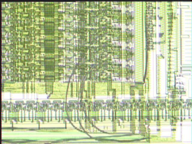
13 Microscope

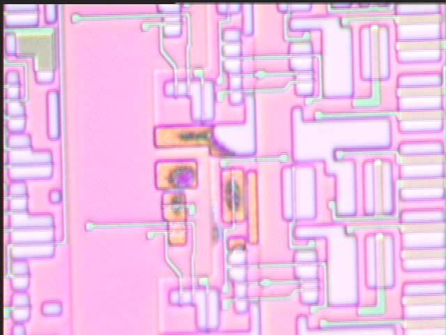
14 Overlay Structure
15 Defects
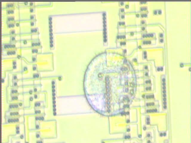
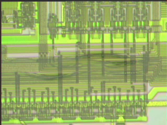
16 Defects
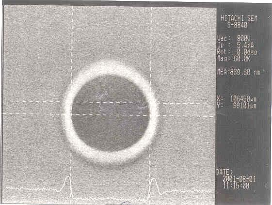
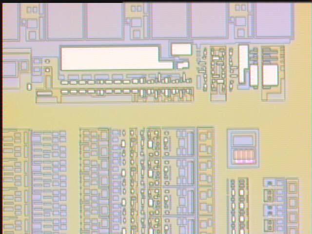
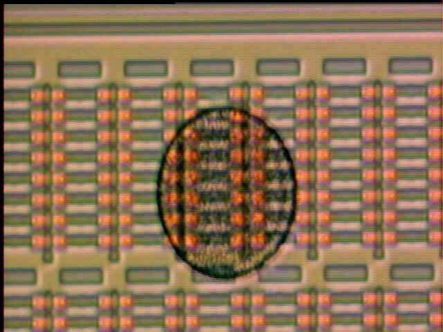
17 CD SEM
18 Process Control
19 Motivation for Photolithography Process Control Factory Cost Leading Edge Exposure Tool Cost Factory capitol cost (USDM) versus Year Cost (USDM) versus Year
20 CD Bias CD bias is the value of CD loss or gain in related to litho patterning and etching process. E.g CD litho = 0.55 um CD after etch = 0.53 um CD bias = um CD bias will determine the CD for litho patterning CD. E.g. Usually specification for CD is for after etch. The litho CD is determined after finding the CD bias.
21 CD Control In high imaging resolution in IC fabrication, the printed CD must be controlled to ever higher precision. CD control can be affected by many parameters, such as illumination, resist transmission and contrast, etc,
22 Photolithography Yield Pyramid Total Yield Process Yield Electrical Yield Defects Overlay Litho Process critical Stability Etch dimension Process Mask Image Contrast Resist Contrast Resist masking Substrate
23 Source of CD Variation Process Apply / Softbake Expose Expose PEB Delay latitude Post Exposure Bake Develop Control Parameter Thickness latitude Dose / Focus latitude PEB Delay Latitude PEB Temp latitude Develop latitude CD Variability ACLV, Xwafer, Xlot, Lotlot ACLV, Xlot, lot-lot ACLV, Xwafer, Xlot, Lotlot ACLV, Xwafer, Xlot, Lotlot Xwafer, Lot-lot
24 Across Chip Linewidth Variation Wavelength 436/ / Groundrule (nm) Within Chip Photofield uniformity Reticle CD uniformity Proximity effect Reflective notching / TFI Total ACLV RSS RSS = root sum square analysis Across-field CD variation can be regarded as largely systematic and can be represent at least 15% (3sigma) of nominal CD.
25 Scanner vs. Stepper
26 Scanner System
27 Scanner vs Stepper Scanner Stepper Resolution * Lens Aberration * Overlay Accuracy = = Mix & Match * Throughput * * Stability * * Price * *: Good
28 Scanner Advantage Smaller Projection Lens Diameter Averaged Effect by Scanning Flexibility for Intra- Field compensation Higher NA Better Lens Aberration Larger DOF Better matching Accuracy
29 Smaller Lens
30 Glossary Reticle - photomask: a master template of IC circuit used for IC fabrication Photomask - same as reticle Pellicle - a membrane mounted on the reticle / photomask to protect the IC designs from contamination and damage. CD -critical dimension is the size of critical pattern fabricated on the wafer. SEM - Scanning Electron Microscope Overlay - the measure of alignment accuracy from one pattern layer to the next pattern layer. Resist - photosensitive chemical used in lithography that changes dissolution properties when exposed to light energy. UV - ultra violet Excimer laser - Short wavelength light source for advance photolithography, 248 nm, 193 nm and 157 nm
31 Glossary I-line - light at wavelength 365 nm g-line - light at wavelength 436 nm swing curve - the plot of exposure dose versus thickness or spin speed smile curve - the plot of dimension versus focus at varying exposure dose CA - chemically amplified resist, the resist for advance photolithography (DUV)
i- Line Photoresist Development: Replacement Evaluation of OiR
 i- Line Photoresist Development: Replacement Evaluation of OiR 906-12 Nishtha Bhatia High School Intern 31 July 2014 The Marvell Nanofabrication Laboratory s current i-line photoresist, OiR 897-10i, has
Photolithography Technology and Application
 Photolithography Technology and Application Jeff Tsai Director, Graduate Institute of Electro-Optical Engineering Tatung University Art or Science? Lind width = 100 to 5 micron meter!! Resolution = ~ 3
Photolithography I ( Part 1 )
") 1 Photolithography I ( Part 1 ) Chapter 13 : Semiconductor Manufacturing Technology by M. Quirk & J. Serda Bjørn-Ove Fimland, Department of Electronics and Telecommunication, Norwegian University of Science
1 Photolithography I ( Part 1 ) Chapter 13 : Semiconductor Manufacturing Technology by M. Quirk & J. Serda Bjørn-Ove Fimland, Department of Electronics and Telecommunication, Norwegian University of Science
Section 2: Lithography. Jaeger Chapter 2 Litho Reader. The lithographic process
 Section 2: Lithography Jaeger Chapter 2 Litho Reader The lithographic process Photolithographic Process (a) (b) (c) (d) (e) (f) (g) Substrate covered with silicon dioxide barrier layer Positive photoresist
Section 2: Lithography. Jaeger Chapter 2 Litho Reader. EE143 Ali Javey Slide 5-1
 Section 2: Lithography Jaeger Chapter 2 Litho Reader EE143 Ali Javey Slide 5-1 The lithographic process EE143 Ali Javey Slide 5-2 Photolithographic Process (a) (b) (c) (d) (e) (f) (g) Substrate covered
Optolith 2D Lithography Simulator
 2D Lithography Simulator Advanced 2D Optical Lithography Simulator 4/13/05 Introduction is a powerful non-planar 2D lithography simulator that models all aspects of modern deep sub-micron lithography It
Major Fabrication Steps in MOS Process Flow
 Major Fabrication Steps in MOS Process Flow UV light Mask oxygen Silicon dioxide photoresist exposed photoresist oxide Silicon substrate Oxidation (Field oxide) Photoresist Coating Mask-Wafer Alignment
Semiconductor Manufacturing Technology. Semiconductor Manufacturing Technology. Photolithography: Resist Development and Advanced Lithography
 Semiconductor Manufacturing Technology Michael Quirk & Julian Serda October 2001 by Prentice Hall Chapter 15 Photolithography: Resist Development and Advanced Lithography Eight Basic Steps of Photolithography
Photolithography II ( Part 2 )
") 1 Photolithography II ( Part 2 ) Chapter 14 : Semiconductor Manufacturing Technology by M. Quirk & J. Serda Saroj Kumar Patra, Department of Electronics and Telecommunication, Norwegian University of Science
1 Photolithography II ( Part 2 ) Chapter 14 : Semiconductor Manufacturing Technology by M. Quirk & J. Serda Saroj Kumar Patra, Department of Electronics and Telecommunication, Norwegian University of Science
Lithography. 3 rd. lecture: introduction. Prof. Yosi Shacham-Diamand. Fall 2004
 Lithography 3 rd lecture: introduction Prof. Yosi Shacham-Diamand Fall 2004 1 List of content Fundamental principles Characteristics parameters Exposure systems 2 Fundamental principles Aerial Image Exposure
Optical Lithography. Keeho Kim Nano Team / R&D DongbuAnam Semi
 Optical Lithography Keeho Kim Nano Team / R&D DongbuAnam Semi Contents Lithography = Photolithography = Optical Lithography CD : Critical Dimension Resist Pattern after Development Exposure Contents Optical
Key Photolithographic Outputs
 Exposure latitude Depth of Focus Exposure latitude Vs DOF plot Linearity and MEEF Isolated-Dense Bias NILS Contrast Swing Curve Reflectivity Curve 1 Exposure latitude:the range of exposure energies (usually
Organic Antireflective Coatings for Photomask Fabrication using Optical Pattern Generators
 Organic Antireflective Coatings for Photomask Fabrication using Optical Pattern Generators Benjamen M. Rathsack 1, Cyrus E. Tabery 1, Cece Philbin 2, and C. Grant Willson 1 September 15, 1999 1 Department
Part 5-1: Lithography
 Part 5-1: Lithography Yao-Joe Yang 1 Pattern Transfer (Patterning) Types of lithography systems: Optical X-ray electron beam writer (non-traditional, no masks) Two-dimensional pattern transfer: limited
Holistic View of Lithography for Double Patterning. Skip Miller ASML
 Holistic View of Lithography for Double Patterning Skip Miller ASML Outline Lithography Requirements ASML Holistic Lithography Solutions Conclusions Slide 2 Shrink Continues Lithography keeps adding value
EE143 Fall 2016 Microfabrication Technologies. Lecture 3: Lithography Reading: Jaeger, Chap. 2
 EE143 Fall 2016 Microfabrication Technologies Lecture 3: Lithography Reading: Jaeger, Chap. 2 Prof. Ming C. Wu wu@eecs.berkeley.edu 511 Sutardja Dai Hall (SDH) 1-1 The lithographic process 1-2 1 Photolithographic
immersion optics Immersion Lithography with ASML HydroLith TWINSCAN System Modifications for Immersion Lithography by Bob Streefkerk
 immersion optics Immersion Lithography with ASML HydroLith by Bob Streefkerk For more than 25 years, many in the semiconductor industry have predicted the end of optical lithography. Recent developments,
MICRO AND NANOPROCESSING TECHNOLOGIES
 MICRO AND NANOPROCESSING TECHNOLOGIES LECTURE 4 Optical lithography Concepts and processes Lithography systems Fundamental limitations and other issues Photoresists Photolithography process Process parameter
MICROBUMP LITHOGRAPHY FOR 3D STACKING APPLICATIONS
 MICROBUMP LITHOGRAPHY FOR 3D STACKING APPLICATIONS Patrick Jaenen, John Slabbekoorn, Andy Miller IMEC Kapeldreef 75 B-3001 Leuven, Belgium millera@imec.be Warren W. Flack, Manish Ranjan, Gareth Kenyon,
Photolithography. References: Introduction to Microlithography Thompson, Willson & Bowder, 1994
 Photolithography References: Introduction to Microlithography Thompson, Willson & Bowder, 1994 Microlithography, Science and Technology Sheats & Smith, 1998 Any other Microlithography or Photolithography
The End of Thresholds: Subwavelength Optical Linewidth Measurement Using the Flux-Area Technique
 The End of Thresholds: Subwavelength Optical Linewidth Measurement Using the Flux-Area Technique Peter Fiekowsky Automated Visual Inspection, Los Altos, California ABSTRACT The patented Flux-Area technique
450mm patterning out of darkness Backend Process Exposure Tool SOKUDO Lithography Breakfast Forum July 10, 2013 Doug Shelton Canon USA Inc.
 450mm patterning out of darkness Backend Process Exposure Tool SOKUDO Lithography Breakfast Forum 2013 July 10, 2013 Doug Shelton Canon USA Inc. Introduction Half Pitch [nm] 2013 2014 2015 2016 2017 2018
Contrast Enhancement Materials CEM 365HR
 INTRODUCTION In 1989 Shin-Etsu Chemical acquired MicroSi, Inc. including their Contrast Enhancement Material (CEM) technology business*. A concentrated effort in the technology advancement of a CEM led
Section 2: Lithography. Jaeger Chapter 2. EE143 Ali Javey Slide 5-1
 Section 2: Lithography Jaeger Chapter 2 EE143 Ali Javey Slide 5-1 The lithographic process EE143 Ali Javey Slide 5-2 Photolithographic Process (a) (b) (c) (d) (e) (f) (g) Substrate covered with silicon
DOE Project: Resist Characterization
 DOE Project: Resist Characterization GOAL To achieve high resolution and adequate throughput, a photoresist must possess relatively high contrast and sensitivity to exposing radiation. The objective of
5. Lithography. 1. photolithography intro: overall, clean room 2. principle 3. tools 4. pattern transfer 5. resolution 6. next-gen
 5. Lithography 1. photolithography intro: overall, clean room 2. principle 3. tools 4. pattern transfer 5. resolution 6. next-gen References: Semiconductor Devices: Physics and Technology. 2 nd Ed. SM
Lecture 7. Lithography and Pattern Transfer. Reading: Chapter 7
 Lecture 7 Lithography and Pattern Transfer Reading: Chapter 7 Used for Pattern transfer into oxides, metals, semiconductors. 3 types of Photoresists (PR): Lithography and Photoresists 1.) Positive: PR
MICROCHIP MANUFACTURING by S. Wolf
 MICROCHIP MANUFACTURING by S. Wolf Chapter 19 LITHOGRAPHY II: IMAGE-FORMATION and OPTICAL HARDWARE 2004 by LATTICE PRESS CHAPTER 19 - CONTENTS Preliminaries: Wave- Motion & The Behavior of Light Resolution
Lecture 8. Microlithography
 Lecture 8 Microlithography Lithography Introduction Process Flow Wafer Exposure Systems Masks Resists State of the Art Lithography Next Generation Lithography (NGL) Recommended videos: http://www.youtube.com/user/asmlcompany#p/search/1/jh6urfqt_d4
Reducing Proximity Effects in Optical Lithography
 INTERFACE '96 This paper was published in the proceedings of the Olin Microlithography Seminar, Interface '96, pp. 325-336. It is made available as an electronic reprint with permission of Olin Microelectronic
Lithographic Process Evaluation by CD-SEM
 Lithographic Process Evaluation by CD-SEM Jason L. Burkholder Microelectronic Engineering Rochester Institute of Technology Rochester, NY 14623 Abstract-- In lithography employed in IC fabrication, focus
Copyright 2000, Society of Photo-Optical Instrumentation Engineers This paper was published in Optical Microlithography XIII, Volume 4000 and is made
 Copyright 00, Society of Photo-Optical Instrumentation Engineers This paper was published in Optical Microlithography XIII, Volume 4000 and is made available as an electronic reprint with permission of
OPC Rectification of Random Space Patterns in 193nm Lithography
 OPC Rectification of Random Space Patterns in 193nm Lithography Mosong Cheng, Andrew Neureuther, Keeho Kim*, Mark Ma*, Won Kim*, Maureen Hanratty* Department of Electrical Engineering and Computer Sciences
Device Fabrication: Photolithography
 Device Fabrication: Photolithography 1 Objectives List the four components of the photoresist Describe the difference between +PR and PR Describe a photolithography process sequence List four alignment
Feature-level Compensation & Control
 Feature-level Compensation & Control 2 Sensors and Control Nathan Cheung, Kameshwar Poolla, Costas Spanos Workshop 11/19/2003 3 Metrology, Control, and Integration Nathan Cheung, UCB SOI Wafers Multi wavelength
Lithography Is the Designer s Brush. Lithography is indispensible for defining locations and configurations of circuit elements/functions.
 Lithography 1 Lithography Is the Designer s Brush Lithography is indispensible for defining locations and configurations of circuit elements/functions. 2 ITRS 2007 The major challenge in litho: CD, CD
Performance data of a new 248 nm CD metrology tool proved on COG reticles and PSM s
 Performance data of a new 248 nm CD metrology tool proved on COG reticles and PSM s Gerhard Schlueter a, Walter Steinberg a, John Whittey b a Leica Microsystems Wetzlar GmbH Ernst-Leitz-Str. 17-37, D-35578
ECSE 6300 IC Fabrication Laboratory Lecture 3 Photolithography. Lecture Outline
 ECSE 6300 IC Fabrication Laboratory Lecture 3 Photolithography Prof. James J. Q. Lu Bldg. CII, Rooms 6229 Rensselaer Polytechnic Institute Troy, NY 12180 Tel. (518)276 2909 e mails: luj@rpi.edu http://www.ecse.rpi.edu/courses/s18/ecse
Lithography. Development of High-Quality Attenuated Phase-Shift Masks
 Lithography S P E C I A L Development of High-Quality Attenuated Phase-Shift Masks by Toshihiro Ii and Masao Otaki, Toppan Printing Co., Ltd. Along with the year-by-year acceleration of semiconductor device
TECHNOLOGY ROADMAP 2006 UPDATE LITHOGRAPHY FOR
 INTERNATIONAL TECHNOLOGY ROADMAP FOR SEMICONDUCTORS 2006 UPDATE LITHOGRAPHY THE ITRS IS DEVISED AND INTENDED FOR TECHNOLOGY ASSESSMENT ONLY AND IS WITHOUT REGARD TO ANY COMMERCIAL CONSIDERATIONS PERTAINING
(Ar [ Si O Si O] m )n
![(Ar [ Si O Si O] m )n](/thumbs/92/107823570.jpg "(Ar [ Si O Si O] m )n") The widespread adoption of advanced packaging techniques is primarily driven by electrical device performance and chip form factor considerations. Flip chip packaging is currently growing at a 27% compound
The widespread adoption of advanced packaging techniques is primarily driven by electrical device performance and chip form factor considerations. Flip chip packaging is currently growing at a 27% compound
2009 International Workshop on EUV Lithography
 Contents Introduction Absorber Stack Optimization Non-flatness Correction Blank Defect and Its Mitigation Wafer Printing Inspection Actinic Metrology Cleaning and Repair Status Remaining Issues in EUV
Lecture 5. Optical Lithography
 Lecture 5 Optical Lithography Intro For most of microfabrication purposes the process (e.g. additive, subtractive or implantation) has to be applied selectively to particular areas of the wafer: patterning
Characterization of a Thick Copper Pillar Bump Process
 Characterization of a Thick Copper Pillar Bump Process Warren W. Flack, Ha-Ai Nguyen Ultratech, Inc. San Jose, CA 95126 Elliott Capsuto, Craig McEwen Shin-Etsu MicroSi, Inc. Phoenix, AZ 85044 Abstract
Module 11: Photolithography. Lecture 14: Photolithography 4 (Continued)
") Module 11: Photolithography Lecture 14: Photolithography 4 (Continued) 1 In the previous lecture, we have discussed the utility of the three printing modes, and their relative advantages and disadvantages.
Module 11: Photolithography Lecture 14: Photolithography 4 (Continued) 1 In the previous lecture, we have discussed the utility of the three printing modes, and their relative advantages and disadvantages.
Contrast Enhancement Materials CEM 365iS
 INTRODUCTION In 1989 Shin-Etsu Chemical acquired MicroSi, Inc. and the Contrast Enhancement Material (CEM) technology business from General Electric including a series of patents and technologies*. A concentrated
PHGN/CHEN/MLGN 435/535: Interdisciplinary Silicon Processing Laboratory. Simple Si solar Cell!
 Where were we? Simple Si solar Cell! Two Levels of Masks - photoresist, alignment Etch and oxidation to isolate thermal oxide, deposited oxide, wet etching, dry etching, isolation schemes Doping - diffusion/ion
Outline. 1 Introduction. 2 Basic IC fabrication processes. 3 Fabrication techniques for MEMS. 4 Applications. 5 Mechanics issues on MEMS MDL NTHU
 Outline 1 Introduction 2 Basic IC fabrication processes 3 Fabrication techniques for MEMS 4 Applications 5 Mechanics issues on MEMS 2.2 Lithography Reading: Runyan Chap. 5, or 莊達人 Chap. 7, or Wolf and
Rudolph s JetStep Lithography System Maximizes Throughput while Addressing the Specific Challenges of Advanced Packaging Applications
 Rudolph s JetStep Lithography System Maximizes Throughput while Addressing the Specific Challenges of Advanced Packaging Applications Elvino da Silveira - Rudolph Technologies, Inc. ABSTRACT Rudolph s
Tutor43.doc; Version 8/15/03 T h e L i t h o g r a p h y E x p e r t (November 2003)
") Tutor43.doc; Version /15/03 T h e L i t h o g r a p h y E x p e r t (November 2003) Scattering Bars Chris A. Mack, KLA-Tencor, FINLE Division, Austin, Texas Resolution enhancement technologies refer to
Tutor43.doc; Version /15/03 T h e L i t h o g r a p h y E x p e r t (November 2003) Scattering Bars Chris A. Mack, KLA-Tencor, FINLE Division, Austin, Texas Resolution enhancement technologies refer to
Optical Lithography. Here Is Why. Burn J. Lin SPIE PRESS. Bellingham, Washington USA
 Optical Lithography Here Is Why Burn J. Lin SPIE PRESS Bellingham, Washington USA Contents Preface xiii Chapter 1 Introducing Optical Lithography /1 1.1 The Role of Lithography in Integrated Circuit Fabrication
Opto-Mechanical Equipment of KBTEM: Present Day and the Future
 KBTEM JSC, Minsk, Belarus Opto-Mechanical Equipment of KBTEM: Present Day and the Future Quality Management System Certificate ISO-9001 since 2001 SPIE Member since 2003 www.kb-omo.by Dr. S.Avakaw SEMI
Copyright 1997 by the Society of Photo-Optical Instrumentation Engineers.
 Copyright 1997 by the Society of Photo-Optical Instrumentation Engineers. This paper was published in the proceedings of Microlithographic Techniques in IC Fabrication, SPIE Vol. 3183, pp. 14-27. It is
Pattern Transfer CD-AFM. Resist Features on Poly. Poly Features on Oxide. Quate Group, Stanford University
 Resist Features on Poly Pattern Transfer Poly Features on Oxide CD-AFM The Critical Dimension AFM Boot -Shaped Tip Tip shape is optimized to sense topography on vertical surfaces Two-dimensional feedback
Chapter 6. Photolithography
 Chapter 6 Photolithography 2006/4/10 1 Objectives List the four components of the photoresist Describe the difference between +PR and PR Describe a photolithography process sequence List four alignment
Critical Dimension Enhancement of DUV Photolithography on the ASML 5500/300. Francesca Calderon Miramonte High School August 13th, 2015
 Critical Dimension Enhancement of DUV Photolithography on the ASML 5500/300 Francesca Calderon Miramonte High School August 13th, 2015 1 g-line - 436 nm i-line - 365 nm DUV - 248 nm DUV - 193 nm resolution
Update on 193nm immersion exposure tool
 Update on 193nm immersion exposure tool S. Owa, H. Nagasaka, Y. Ishii Nikon Corporation O. Hirakawa and T. Yamamoto Tokyo Electron Kyushu Ltd. January 28, 2004 Litho Forum 1 What is immersion lithography?
Optical Requirements
 Optical Requirements Transmission vs. Film Thickness A pellicle needs a good light transmission and long term transmission stability. Transmission depends on the film thickness, film material and any anti-reflective
Technology for the MEMS processing and testing environment. SUSS MicroTec AG Dr. Hans-Georg Kapitza
 Technology for the MEMS processing and testing environment SUSS MicroTec AG Dr. Hans-Georg Kapitza 1 SUSS MicroTec Industrial Group Founded 1949 as Karl Süss KG GmbH&Co. in Garching/ Munich San Jose Waterbury
UV Nanoimprint Stepper Technology: Status and Roadmap. S.V. Sreenivasan Sematech Litho Forum May 14 th, 2008
 UV Nanoimprint Stepper Technology: Status and Roadmap S.V. Sreenivasan Sematech Litho Forum May 14 th, 2008 Overview Introduction Stepper technology status: Patterning and CD Control Through Etch Alignment
EE-527: MicroFabrication
 EE-57: MicroFabrication Exposure and Imaging Photons white light Hg arc lamp filtered Hg arc lamp excimer laser x-rays from synchrotron Electrons Ions Exposure Sources focused electron beam direct write
Photolithography 光刻 Part I: Optics
 微纳光电子材料与器件工艺原理 Photolithography 光刻 Part I: Optics Xing Sheng 盛兴 Department of Electronic Engineering Tsinghua University xingsheng@tsinghua.edu.cn 1 Integrate Circuits Moore's law transistor number transistor
Optical Microlithography XXVIII
 PROCEEDINGS OF SPIE Optical Microlithography XXVIII Kafai Lai Andreas Erdmann Editors 24-26 February 2015 San Jose, California, United States Sponsored by SPIE Cosponsored by Cymer, an ASML company (United
Mask Technology Development in Extreme-Ultraviolet Lithography
 Mask Technology Development in Extreme-Ultraviolet Lithography Anthony Yen September 6, 2013 Projected End of Optical Lithography 2013 TSMC, Ltd 1976 1979 1982 1985 1988 1991 1994 1997 2000 2003 2007 2012
INTERNATIONAL TECHNOLOGY ROADMAP SEMICONDUCTORS 2001 EDITION LITHOGRAPHY FOR
 INTERNATIONAL TECHNOLOGY ROADMAP FOR SEMICONDUCTORS 2001 EDITION LITHOGRAPHY TABLE OF CONTENTS Scope...1 Difficult Challenges...1 Lithography Technology Requirements...3 Potential Solutions...14 Crosscut
MeRck. AZ nlof technical datasheet. Negative Tone Photoresist for Single Layer Lift-Off APPLICATION TYPICAL PROCESS. SPIN CURVE (150MM Silicon)
") MeRck technical datasheet AZ nlof 5510 Negative Tone Photoresist for Single Layer Lift-Off APPLICATION AZ nlof 5510 i-line photoresist is engineered to simplify the historically complex image reversal
MeRck technical datasheet AZ nlof 5510 Negative Tone Photoresist for Single Layer Lift-Off APPLICATION AZ nlof 5510 i-line photoresist is engineered to simplify the historically complex image reversal
Characterization Study of an Aqueous Developable Photosensitive Polyimide on 300 mm Wafers
 Characterization Study of an Aqueous Developable Photosensitive Polyimide on 300 mm Wafers Warren W. Flack, Scott Kulas Ultratech Stepper, Inc. San Jose, CA 95134 Craig Franklin HD Microsystems Austin,
Ion Beam Lithography next generation nanofabrication
 Ion Beam Lithography next generation nanofabrication EFUG Bordeaux 2011 ion beams develop Lloyd Peto IBL sales manager Copyright 2011 by Raith GmbH ionline new capabilities You can now Apply an ion beam
Dr. Dirk Meyners Prof. Wagner. Wagner / Meyners Micro / Nanosystems Technology
 Micro/Nanosystems Technology Dr. Dirk Meyners Prof. Wagner 1 Outline - Lithography Overview - UV-Lithography - Resolution Enhancement Techniques - Electron Beam Lithography - Patterning with Focused Ion
Advanced Stepper Lithography Technology to Enable Flexible AMOLED Displays. Keith Best Roger McCleary Elvino M da Silveira 5/19/17
 Advanced Stepper Lithography Technology to Enable Flexible AMOLED Displays Keith Best Roger McCleary Elvino M da Silveira 5/19/17 Agenda About Rudolph JetStep G System overview and performance Display
Lithographic Performance and Mix-and-Match Lithography using 100 kv Electron Beam System JBX-9300FS
 Lithographic Performance and Mix-and-Match Lithography using 100 kv Electron Beam System JBX-9300FS Yukinori Ochiai, Takashi Ogura, Mitsuru Narihiro, and Kohichi Arai Silicon Systems Research Laboratories,
UV LED ILLUMINATION STEPPER OFFERS HIGH PERFORMANCE AND LOW COST OF OWNERSHIP
 UV LED ILLUMINATION STEPPER OFFERS HIGH PERFORMANCE AND LOW COST OF OWNERSHIP Casey Donaher, Rudolph Technologies Herbert J. Thompson, Rudolph Technologies Chin Tiong Sim, Rudolph Technologies Rudolph
Advanced Packaging Lithography and Inspection Solutions for Next Generation FOWLP-FOPLP Processing
 Advanced Packaging Lithography and Inspection Solutions for Next Generation FOWLP-FOPLP Processing Keith Best, Gurvinder Singh, and Roger McCleary Rudolph Technologies, Inc. 16 Jonspin Rd. Wilmington,
MeRck. nlof 2000 Series. technical datasheet. Negative Tone Photoresists for Single Layer Lift-Off APPLICATION TYPICAL PROCESS
 MeRck technical datasheet AZ Negative Tone Photoresists for Single Layer Lift-Off APPLICATION AZ i-line photoresists are engineered to simplify the historically complex image reversal and multilayer lift-off
Positive-Tone Photosensitive Polyimide Coatings for Lens Layer in image sensors. Introduction of the characteristic of CS-series
 Positive-Tone Photosensitive Polyimide Coatings for Lens Layer in image sensors Photoneece CS-series Introduction of the characteristic of CS-series Toray Industries, Inc. 1 1 CS-7500 basic properties
Lecture 13 Basic Photolithography
 Lecture 13 Basic Photolithography Chapter 12 Wolf and Tauber 1/64 Announcements Homework: Homework 3 is due today, please hand them in at the front. Will be returned one week from Thursday (16 th Nov).
KrF EXCIMER LASER LITHOGRAPHY TECHNOLOGY FOR 64MDRAM
 Journa' of Photopolymer Science and Technology Volume 4, Number 3 (1991) 361-369 KrF EXCIMER LASER LITHOGRAPHY TECHNOLOGY FOR 64MDRAM MASAYUKI ENDO, YOSHIYUKI TAM, TOSHIKI YABU, SHOZO OKADA MASARU SASAGO
Synthesis of projection lithography for low k1 via interferometry
 Synthesis of projection lithography for low k1 via interferometry Frank Cropanese *, Anatoly Bourov, Yongfa Fan, Andrew Estroff, Lena Zavyalova, Bruce W. Smith Center for Nanolithography Research, Rochester
ADVANCED MASK MAKING AT RIT. David P. Kanen 5th Year Microelectronic Engineer Student Rochester Institute of Technology ABSTRACT
 ADVANCED MASK MAKING AT RIT David P. Kanen 5th Year Microelectronic Engineer Student Rochester Institute of Technology ABSTRACT This project involved the definition of the steps necessary to generate a
Chapter 6 Photolithography
 Chapter 6 Photolithography Hong Xiao, Ph. D. hxiao89@hotmail.com www2.austin.cc.tx.us/hongxiao/book.htm Hong Xiao, Ph. D. www2.austin.cc.tx.us/hongxiao/book.htm 1 Objectives List the four components of
Lithography Simulation Tools Needed for 22nm HP and Beyond. Chris Mack
 Lithography Simulation Tools Needed for 22nm HP and Beyond Chris Mack www.lithoguru.com Slicing the Pie Simulation Tool Characteristics Precision Accuracy Capabilities (speed, features) Simulation Tool
Microlens formation using heavily dyed photoresist in a single step
 Microlens formation using heavily dyed photoresist in a single step Chris Cox, Curtis Planje, Nick Brakensiek, Zhimin Zhu, Jonathan Mayo Brewer Science, Inc., 2401 Brewer Drive, Rolla, MO 65401, USA ABSTRACT
Analysis of Focus Errors in Lithography using Phase-Shift Monitors
 Draft paper for SPIE Conference on Microlithography (Optical Lithography) 6/6/2 Analysis of Focus Errors in Lithography using Phase-Shift Monitors Bruno La Fontaine *a, Mircea Dusa **b, Jouke Krist b,
Immersion Lithography: New Opportunities for Semiconductor Manufacturing
 Immersion Lithography: New Opportunities for Semiconductor Manufacturing Tim Brunner, Dario Gil, Carlos Fonseca and Nakgeuon Seong IBM - SRDC Bob Streefkerk, Christian Wagner and Marco Stavenga ASML Outline
1X Broadband Wafer Stepper for Bump and Wafer Level Chip Scale Packaging (CSP) Applications
 Applications") 1X Broadband Wafer Stepper for Bump and Wafer Level Chip Scale Packaging (CSP) Applications Doug Anberg, Mitch Eguchi, Takahiro Momobayashi Ultratech Stepper, Inc. San Jose, California Takeshi Wakabayashi,
1X Broadband Wafer Stepper for Bump and Wafer Level Chip Scale Packaging (CSP) Applications Doug Anberg, Mitch Eguchi, Takahiro Momobayashi Ultratech Stepper, Inc. San Jose, California Takeshi Wakabayashi,
Managing Within Budget
 Overlay M E T R O L OProcess G Y Control Managing Within Budget Overlay Metrology Accuracy in a 0.18 µm Copper Dual Damascene Process Bernd Schulz and Rolf Seltmann, AMD Saxony Manufacturing GmbH, Harry
Module - 2 Lecture - 13 Lithography I
 Nano Structured Materials-Synthesis, Properties, Self Assembly and Applications Prof. Ashok. K.Ganguli Department of Chemistry Indian Institute of Technology, Delhi Module - 2 Lecture - 13 Lithography
High-resolution microlithography using a 193nm excimer laser source. Nadeem H. Rizvi, Dominic Ashworth, Julian S. Cashmore and Malcolm C.
 High-resolution microlithography using a 193nm excimer laser source. Nadeem H. Rizvi, Dominic Ashworth, Julian S. Cashmore and Malcolm C. Gower Exitech Limited Hanborough Park, Long Hanborough, Oxford
Development of a LFLE Double Pattern Process for TE Mode Photonic Devices. Mycahya Eggleston Advisor: Dr. Stephen Preble
 Development of a LFLE Double Pattern Process for TE Mode Photonic Devices Mycahya Eggleston Advisor: Dr. Stephen Preble 2 Introduction and Motivation Silicon Photonics Geometry, TE vs TM, Double Pattern
Lithographic Performance of a New Generation i-line Optical System: A Comparative Analysis. Abstract
 Lithographic Performance of a New Generation i-line Optical System: A Comparative Analysis Gary Flores, Warren Flack, Lynn Dwyer Ultratech Stepper 3230 Scott Blvd. Santa Clara CA 95054 Abstract A new generation
Copyright 1998 by the Society of Photo-Optical Instrumentation Engineers.
 Copyright 998 by the Society of Photo-Optical Instrumentation Engineers. This paper was published in the proceedings of the 8 th Annual BACUS Symposium on Photomask Technology and Management SPIE Vol.
Applications of Maskless Lithography for the Production of Large Area Substrates Using the SF-100 ELITE. Jay Sasserath, PhD
 Applications of Maskless Lithography for the Production of Large Area Substrates Using the SF-100 ELITE Executive Summary Jay Sasserath, PhD Intelligent Micro Patterning LLC St. Petersburg, Florida Processing
Comparative Study of Binary Intensity Mask and Attenuated Phase Shift Mask using Hyper-NA Immersion Lithography for Sub-45nm Era
 Comparative Study of Binary Intensity Mask and Attenuated Phase Shift Mask using Hyper-NA Immersion Lithogr for Sub-45nm Era Tae-Seung Eom*, Jun-Taek Park, Sarohan Park, Sunyoung Koo, Jin-Soo Kim, Byoung-Hoon
Innovative Mask Aligner Lithography for MEMS and Packaging
 Innovative Mask Aligner Lithography for MEMS and Packaging Dr. Reinhard Voelkel CEO SUSS MicroOptics SA September 9 th, 2010 1 SUSS Micro-Optics SUSS MicroOptics is a leading supplier for high-quality
Progresses in NIL Template Fabrication Naoya Hayashi
 Progresses in NIL Template Fabrication Naoya Hayashi Electronic Device Operations Dai Nippon Printing Co., Ltd. Contents 1. Introduction Motivation NIL mask fabrication process 2. NIL mask resolution improvement
optical and photoresist effects
 Focus effects in submicron optical lithography, optical and photoresist effects Chris A. Mack and Patricia M. Kaufman Department of Defense Fort Meade, Maryland 20755 Abstract This paper gives a review
16nm with 193nm Immersion Lithography and Double Exposure
 16nm with 193nm Immersion Lithography and Double Exposure Valery Axelrad, Sequoia Design Systems, Inc. (United States) Michael C. Smayling, Tela Innovations, Inc. (United States) ABSTRACT Gridded Design
Discovering Electrical & Computer Engineering. Carmen S. Menoni Professor Week 3 armain.
 Discovering Electrical & Computer Engineering Carmen S. Menoni Professor Week 3 http://www.engr.colostate.edu/ece103/semin armain.html TOP TECH 2012 SPECIAL REPORT IEEE SPECTRUM PAGE 28, JANUARY 2012 P.E.
TECHNOLOGY ROADMAP 2005 EDITION LITHOGRAPHY FOR
 INTERNATIONAL TECHNOLOGY ROADMAP FOR SEMICONDUCTORS 2005 EDITION LITHOGRAPHY THE ITRS IS DEVISED AND INTENDED FOR TECHNOLOGY ASSESSMENT ONLY AND IS WITHOUT REGARD TO ANY COMMERCIAL CONSIDERATIONS PERTAINING
Next-generation DUV light source technologies for 10nm and below
 Next-generation DUV light source technologies for 10nm and below Ted Cacouris, Greg Rechtsteiner, Will Conley Cymer LLC, 17075 Thornmint Court, San Diego, CA 92127 ABSTRACT Multi-patterning techniques