Critical Dimension Enhancement of DUV Photolithography on the ASML 5500/300. Francesca Calderon Miramonte High School August 13th, 2015
|
|
|
- Sabina Hood
- 5 years ago
- Views:
Transcription


1 Critical Dimension Enhancement of DUV Photolithography on the ASML 5500/300 Francesca Calderon Miramonte High School August 13th,
![g-line - 436 nm i-line - 365 nm DUV - 248 nm DUV - 193 nm resolution ~ λ /2NA [1] Krassenstein, Brian.](/docs-images/83/88392973/images/2-0.jpg "\"The Moore s Law of 3D Printing Yes It Does Exist, And Could Have Staggering Implications.\" 3DPrintcom. N.p., 28 June 2014.")
2 g-line nm i-line nm DUV nm DUV nm resolution ~ λ /2NA [1] Krassenstein, Brian. "The Moore s Law of 3D Printing Yes It Does Exist, And Could Have Staggering Implications." 3DPrintcom. N.p., 28 June Web. 12 Aug

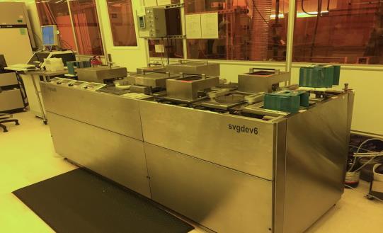
3 Photolithography Review Bottom Anti Reflective Coating - svgcoat3 Photoresist Coat - svgcoat6 DUV Exposure - asml300 Develop in MF26 - svgdev6 UV stabilize - axcelis/uv bake [2] "Semiconductor Lithography." The Basics of Microlithography. N.p., 23 Nov Web. 03 Aug
4 Background and History It is understood that the current resolution limit of the asml300 is 250 nm The past baseline CMOS runs have successfully made transistors with 350 nm features Similar systems in other labs have been shown to go down to 200 nm for an isolated line 4
![Background: Optical Coln in Stepper [3] Ito, Takashi, and](/docs-images/83/88392973/images/5-0.jpg "Shinji Okazaki. Nature. N.p., 31 Aug. 2000. Web. 12 Aug.")
5 Background: Optical Coln in Stepper [3] Ito, Takashi, and Shinji Okazaki. Nature. N.p., 31 Aug Web. 12 Aug


6 Theory: Annular Illination [3] Ito, Takashi, and Shinji Okazaki. Nature. N.p., 31 Aug Web. 12 Aug
7 Goals Characterize properties of UV , a new photoresist generate a process specification for lab members to reference Determine the minim feature size that can be produced on the asml300 Focus-exposure matrices and inspection with leo SEM Characterize off-axis illination and variable nerical aperture Bossung and exposure latitude plots 7

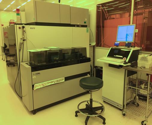
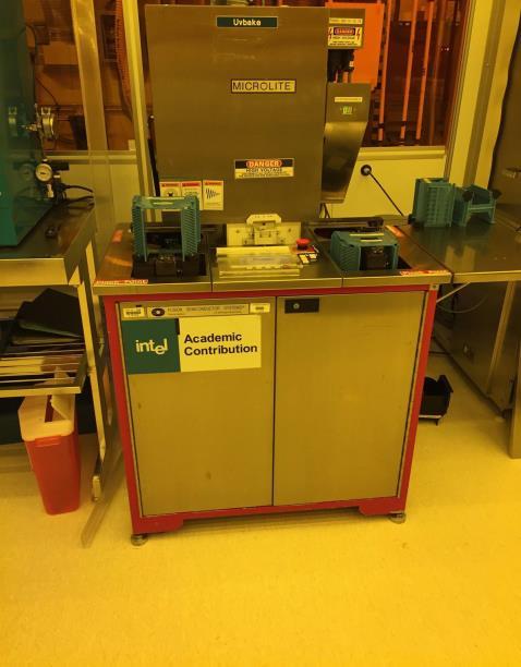
8 Tools Qualified On : svgcoat/dev6 svgcoat3 axcelis uvbake asml300 8


9 Tools Qualified On : nanospec matrix asiq primeoven leo 9


10 Experimental Method - Photoresist Characterization 1. Coated wafers at different spin speeds and measured film thickness generate spin speed curve 2. Decided upon a spin speed to achieve a targeted film thickness 3. Created a process specification to define the final process 4. Ran process wafers to populate the process specification 10
11 Experimental Results - Photoresist Characterization The vendor data sheet provided a spin speed curve that closely matched our experimental results on svgcoat6 11

12 Experimental Results - Process Specification 12


13 Experimental Method - Critical Dimension Enhancement 1. Ran focus-exposure matrices 2. Measured linewidth with the leo SEM 3. Created Bossung and exposure latitude plots 4. Determined ideal imaging conditions to resolve 150 nm isolated lines 5. Patterned whole wafers with ideal conditions to make sure the results were repeatable 13
14 Intro to Bossung Plots What is important: 1. A change in exposure dose results in the smallest possible change in linewidth - ΔY 2. A change in focus results in the smallest possible change in linewidth - slope 14
15 Intro to Exposure Latitude Plots What is important: 1. A change in focus dose results in the smallest possible change in linewidth - ΔY 2. A change in exposure results in the smallest possible change in linewidth - slope 15
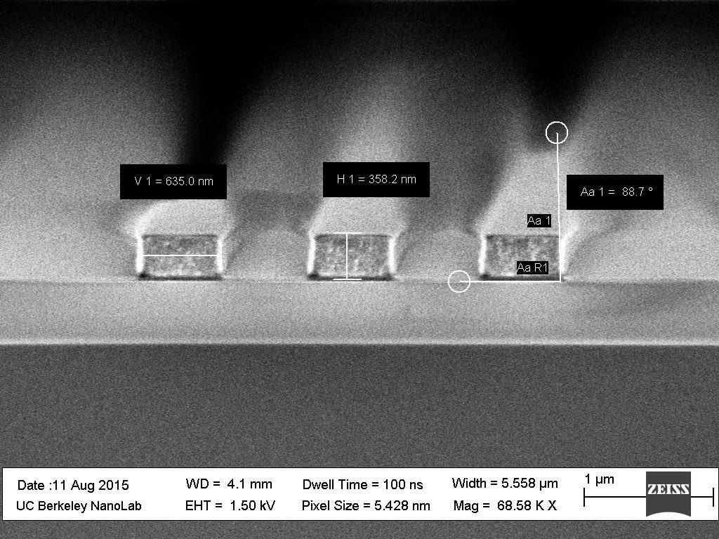
16 Experimental Results - Conventional Imaging Dose: 13 Focus: Enhancement: none Exposure Latitude: 186 nm nm = 69 nm 16
17 Experimental Results - Critical Dimension Enhancement Dose: 16 Focus: Enhancement: NA = 0.6 Outer = Inner = Exposure Latitude: nm nm = 9.5 nm 17
18 Experimental Results - Critical Dimension Enhancement Dose: 16 Focus: Enhancement: NA = 0.6 Outer = Inner = Exposure Latitude: 161 nm nm = 3.5 nm 18
19 Chosen Image Settings Exposure: 16 Focus: microns Nerical Aperture: 0.6 Annular Condition 1: Sigma Inner: Sigma Outer: Annular Condition 2: Sigma Inner: Sigma Outer


20 Experimental Results : Wafer Scale Performance, CD = 150 nm 21 locations per wafer were measured Best case imaging was observed with the small annular ring. It produced an average line width of nm, with a 90.5% yield. 20

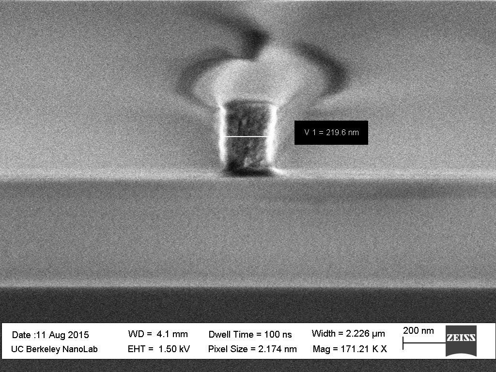
21 Experimental Results : UV Cross-sectional Profiles line width = 152 nm sidewall angle = 90º aspect ratio ~ 2.5:1 Imaging conditions: 16, -0.23, NA=0.6 Sigma Outer=0.855 Sigma Inner=
22 Conclusion 150 nm lines have been resolved in 3800 Å thick UV photoresist The results found are consistent from wafer-towafer and uniform across a wafer CD fidelity has good accuracy with the average line width less than 1 nm from target and a standard deviation approximately 11 nm 22


23 Acknowledgements - Thank You! Jeff Clarkson Kim Chan Irving Garduno Greg Mullins David Lo Cheryl Chang Marilyn Kushner Bill Flounders 23
24 24
i- Line Photoresist Development: Replacement Evaluation of OiR
 i- Line Photoresist Development: Replacement Evaluation of OiR 906-12 Nishtha Bhatia High School Intern 31 July 2014 The Marvell Nanofabrication Laboratory s current i-line photoresist, OiR 897-10i, has
Optolith 2D Lithography Simulator
 2D Lithography Simulator Advanced 2D Optical Lithography Simulator 4/13/05 Introduction is a powerful non-planar 2D lithography simulator that models all aspects of modern deep sub-micron lithography It
Copyright 1997 by the Society of Photo-Optical Instrumentation Engineers.
 Copyright 1997 by the Society of Photo-Optical Instrumentation Engineers. This paper was published in the proceedings of Microlithographic Techniques in IC Fabrication, SPIE Vol. 3183, pp. 14-27. It is
DOE Project: Resist Characterization
 DOE Project: Resist Characterization GOAL To achieve high resolution and adequate throughput, a photoresist must possess relatively high contrast and sensitivity to exposing radiation. The objective of
Tutor43.doc; Version 8/15/03 T h e L i t h o g r a p h y E x p e r t (November 2003)
") Tutor43.doc; Version /15/03 T h e L i t h o g r a p h y E x p e r t (November 2003) Scattering Bars Chris A. Mack, KLA-Tencor, FINLE Division, Austin, Texas Resolution enhancement technologies refer to
Tutor43.doc; Version /15/03 T h e L i t h o g r a p h y E x p e r t (November 2003) Scattering Bars Chris A. Mack, KLA-Tencor, FINLE Division, Austin, Texas Resolution enhancement technologies refer to
(ksaligner & quintel resolution)
") Process [4.10] (ksaligner & quintel resolution) 1.0 Process Summary 1.1 Since Karl Suss ksaligner is heavily used and Quintel aligner is not, nanolab decided to compare the 2 micron line resolution from
Process [4.10] (ksaligner & quintel resolution) 1.0 Process Summary 1.1 Since Karl Suss ksaligner is heavily used and Quintel aligner is not, nanolab decided to compare the 2 micron line resolution from
Photolithography I ( Part 1 )
") 1 Photolithography I ( Part 1 ) Chapter 13 : Semiconductor Manufacturing Technology by M. Quirk & J. Serda Bjørn-Ove Fimland, Department of Electronics and Telecommunication, Norwegian University of Science
1 Photolithography I ( Part 1 ) Chapter 13 : Semiconductor Manufacturing Technology by M. Quirk & J. Serda Bjørn-Ove Fimland, Department of Electronics and Telecommunication, Norwegian University of Science
Reducing Proximity Effects in Optical Lithography
 INTERFACE '96 This paper was published in the proceedings of the Olin Microlithography Seminar, Interface '96, pp. 325-336. It is made available as an electronic reprint with permission of Olin Microelectronic
Copyright 2000, Society of Photo-Optical Instrumentation Engineers This paper was published in Optical Microlithography XIII, Volume 4000 and is made
 Copyright 00, Society of Photo-Optical Instrumentation Engineers This paper was published in Optical Microlithography XIII, Volume 4000 and is made available as an electronic reprint with permission of
MEMORANDUM. This is a summary of the activities and projects that I was involved in during 2009.
 MEMORANDUM To: Katalin Voros, Operations Manager From: Kim Chan, Assistant Development Engineer Subject: 2009 Year-End Report Date: 15 January 2010 cc: Sia Parsa, Andy Neureuther This is a summary of the
Process Optimization
 Process Optimization Process Flow for non-critical layer optimization START Find the swing curve for the desired resist thickness. Determine the resist thickness (spin speed) from the swing curve and find
Lithographic Process Evaluation by CD-SEM
 Lithographic Process Evaluation by CD-SEM Jason L. Burkholder Microelectronic Engineering Rochester Institute of Technology Rochester, NY 14623 Abstract-- In lithography employed in IC fabrication, focus
Key Photolithographic Outputs
 Exposure latitude Depth of Focus Exposure latitude Vs DOF plot Linearity and MEEF Isolated-Dense Bias NILS Contrast Swing Curve Reflectivity Curve 1 Exposure latitude:the range of exposure energies (usually
What s So Hard About Lithography?
 What s So Hard About Lithography? Chris A. Mack, www.lithoguru.com, Austin, Texas Optical lithography has been the mainstay of semiconductor patterning since the early days of integrated circuit production.
MICROBUMP LITHOGRAPHY FOR 3D STACKING APPLICATIONS
 MICROBUMP LITHOGRAPHY FOR 3D STACKING APPLICATIONS Patrick Jaenen, John Slabbekoorn, Andy Miller IMEC Kapeldreef 75 B-3001 Leuven, Belgium millera@imec.be Warren W. Flack, Manish Ranjan, Gareth Kenyon,
MICRO AND NANOPROCESSING TECHNOLOGIES
 MICRO AND NANOPROCESSING TECHNOLOGIES LECTURE 4 Optical lithography Concepts and processes Lithography systems Fundamental limitations and other issues Photoresists Photolithography process Process parameter
optical and photoresist effects
 Focus effects in submicron optical lithography, optical and photoresist effects Chris A. Mack and Patricia M. Kaufman Department of Defense Fort Meade, Maryland 20755 Abstract This paper gives a review
MICROCHIP MANUFACTURING by S. Wolf
 MICROCHIP MANUFACTURING by S. Wolf Chapter 19 LITHOGRAPHY II: IMAGE-FORMATION and OPTICAL HARDWARE 2004 by LATTICE PRESS CHAPTER 19 - CONTENTS Preliminaries: Wave- Motion & The Behavior of Light Resolution
Depth of Focus, part 2
 T h e L i t h o g r a p h y T u t o r (Autumn 995) Depth of ocus, part Chris A. Mack, INL Technologies, Austin, Texas In the last column we began our search for a suitable definition for depth of focus
Lithographic Performance of a New Generation i-line Optical System: A Comparative Analysis. Abstract
 Lithographic Performance of a New Generation i-line Optical System: A Comparative Analysis Gary Flores, Warren Flack, Lynn Dwyer Ultratech Stepper 3230 Scott Blvd. Santa Clara CA 95054 Abstract A new generation
Using the Normalized Image Log-Slope, part 2
 T h e L i t h o g r a p h y E x p e r t (Spring ) Using the Normalized Image Log-Slope, part Chris A. Mack, FINLE Technologies, A Division of KLA-Tencor, Austin, Texas As we saw in part of this column,
Resolution. T h e L i t h o g r a p h y E x p e r t (Winter 1997) Chris A. Mack, FINLE Technologies, Austin, Texas
 Chris A. Mack, FINLE Technologies, Austin, Texas") T h e L i t h o g r a p h y E x p e r t (Winter 1997) Resolution Chris A. Mack, FINLE Technologies, Austin, Texas In past editions of this column (Spring and Summer, 1995), we defined quite carefully what
T h e L i t h o g r a p h y E x p e r t (Winter 1997) Resolution Chris A. Mack, FINLE Technologies, Austin, Texas In past editions of this column (Spring and Summer, 1995), we defined quite carefully what
Photolithography II ( Part 2 )
") 1 Photolithography II ( Part 2 ) Chapter 14 : Semiconductor Manufacturing Technology by M. Quirk & J. Serda Saroj Kumar Patra, Department of Electronics and Telecommunication, Norwegian University of Science
1 Photolithography II ( Part 2 ) Chapter 14 : Semiconductor Manufacturing Technology by M. Quirk & J. Serda Saroj Kumar Patra, Department of Electronics and Telecommunication, Norwegian University of Science
immersion optics Immersion Lithography with ASML HydroLith TWINSCAN System Modifications for Immersion Lithography by Bob Streefkerk
 immersion optics Immersion Lithography with ASML HydroLith by Bob Streefkerk For more than 25 years, many in the semiconductor industry have predicted the end of optical lithography. Recent developments,
1. INTRODUCTION 2. SCATTEROMETRY BASICS ABSTRACT
 Evaluating the Performance of a 193nm Hyper-NA Immersion Scanner Using Scatterometry Oleg Kritsun a, Bruno La Fontaine a, Richard Sandberg a, Alden Acheta a, Harry J. Levinson a, Kevin Lensing b, Mircea
Analysis of Focus Errors in Lithography using Phase-Shift Monitors
 Draft paper for SPIE Conference on Microlithography (Optical Lithography) 6/6/2 Analysis of Focus Errors in Lithography using Phase-Shift Monitors Bruno La Fontaine *a, Mircea Dusa **b, Jouke Krist b,
Optical Proximity Effects, part 2
 T h e L i t h o g r a p h y E x p e r t (Summer 1996) Optical Proximity Effects, part 2 Chris A. Mack, FINLE Technologies, Austin, Texas In the last edition of the Lithography Expert, we examined one type
Optimizing FinFET Structures with Design-based Metrology
 Lithography M e t r o l o g y Optimizing FinFET Structures with Design-based Metrology Tom Vandeweyer, Christie Delvaux, Johan De Backer, and Monique Ercken, IMEC Gian Lorusso, Radhika Jandhyala, Amir
Effect of Reticle CD Uniformity on Wafer CD Uniformity in the Presence of Scattering Bar Optical Proximity Correction
 Effect of Reticle CD Uniformity on Wafer CD Uniformity in the Presence of Scattering Bar Optical Proximity Correction Konstantinos Adam*, Robert Socha**, Mircea Dusa**, and Andrew Neureuther* *University
Experimental measurement of photoresist modulation curves
 Experimental measurement of photoresist modulation curves Anatoly Bourov *a,c, Stewart A. Robertson b, Bruce W. Smith c, Michael Slocum c, Emil C. Piscani c a Rochester Institute of Technology, 82 Lomb
Discovering Electrical & Computer Engineering. Carmen S. Menoni Professor Week 3 armain.
 Discovering Electrical & Computer Engineering Carmen S. Menoni Professor Week 3 http://www.engr.colostate.edu/ece103/semin armain.html TOP TECH 2012 SPECIAL REPORT IEEE SPECTRUM PAGE 28, JANUARY 2012 P.E.
OPC Rectification of Random Space Patterns in 193nm Lithography
 OPC Rectification of Random Space Patterns in 193nm Lithography Mosong Cheng, Andrew Neureuther, Keeho Kim*, Mark Ma*, Won Kim*, Maureen Hanratty* Department of Electrical Engineering and Computer Sciences
Contrast Enhancement Materials CEM 365HR
 INTRODUCTION In 1989 Shin-Etsu Chemical acquired MicroSi, Inc. including their Contrast Enhancement Material (CEM) technology business*. A concentrated effort in the technology advancement of a CEM led
In-line focus monitoring and fast determination of best focus using scatterometry
 In-line focus monitoring and fast determination of best focus using scatterometry a Steven Thanh Ha, a Benjamin Eynon, a Melany Wynia, a Jeff Schmidt, b Christian Sparka, b Antonio Mani, b Roie Volkovich,
Characterization Study of an Aqueous Developable Photosensitive Polyimide on 300 mm Wafers
 Characterization Study of an Aqueous Developable Photosensitive Polyimide on 300 mm Wafers Warren W. Flack, Scott Kulas Ultratech Stepper, Inc. San Jose, CA 95134 Craig Franklin HD Microsystems Austin,
Copyright 2000 by the Society of Photo-Optical Instrumentation Engineers.
 Copyright by the Society of Photo-Optical Instrumentation Engineers. This paper was published in the proceedings of Optical Microlithography XIII, SPIE Vol. 4, pp. 658-664. It is made available as an electronic
The End of Thresholds: Subwavelength Optical Linewidth Measurement Using the Flux-Area Technique
 The End of Thresholds: Subwavelength Optical Linewidth Measurement Using the Flux-Area Technique Peter Fiekowsky Automated Visual Inspection, Los Altos, California ABSTRACT The patented Flux-Area technique
CONTACT HOLE IMAGING AT THE 0.13 µm NODE USING KrF LITHOGRAPHY
 CONTACT HOLE IMAGING AT THE.13 µm NODE USING KrF LITHOGRAPHY Carsten Kohler, Eelco van Setten, Jo Finders ASML, Veldhoven, The Netherlands This paper was first presented at the Arch Chemicals Seminar,
Resist Process Window Characterization for the 45-nm Node Using an Interferometric Immersion microstepper
 Rochester Institute of Technology RIT Scholar Works Presentations and other scholarship 3-29-2006 Resist Process Window Characterization for the 45-nm Node Using an Interferometric Immersion microstepper
Immersion Lithography: New Opportunities for Semiconductor Manufacturing
 Immersion Lithography: New Opportunities for Semiconductor Manufacturing Tim Brunner, Dario Gil, Carlos Fonseca and Nakgeuon Seong IBM - SRDC Bob Streefkerk, Christian Wagner and Marco Stavenga ASML Outline
Photolithography Technology and Application
 Photolithography Technology and Application Jeff Tsai Director, Graduate Institute of Electro-Optical Engineering Tatung University Art or Science? Lind width = 100 to 5 micron meter!! Resolution = ~ 3
Critical dimension sensitivity to post-exposure bake temperature variation in EUV photoresists
 Critical dimension sensitivity to post-exposure bake temperature variation in EUV photoresists Jason P. Cain, a* Patrick Naulleau, b Costas J. Spanos a a Department of Electrical Engineering and Computer
Contrast Enhancement Materials CEM 365iS
 INTRODUCTION In 1989 Shin-Etsu Chemical acquired MicroSi, Inc. and the Contrast Enhancement Material (CEM) technology business from General Electric including a series of patents and technologies*. A concentrated
ECSE 6300 IC Fabrication Laboratory Lecture 3 Photolithography. Lecture Outline
 ECSE 6300 IC Fabrication Laboratory Lecture 3 Photolithography Prof. James J. Q. Lu Bldg. CII, Rooms 6229 Rensselaer Polytechnic Institute Troy, NY 12180 Tel. (518)276 2909 e mails: luj@rpi.edu http://www.ecse.rpi.edu/courses/s18/ecse
Holistic View of Lithography for Double Patterning. Skip Miller ASML
 Holistic View of Lithography for Double Patterning Skip Miller ASML Outline Lithography Requirements ASML Holistic Lithography Solutions Conclusions Slide 2 Shrink Continues Lithography keeps adding value
Lithography. 3 rd. lecture: introduction. Prof. Yosi Shacham-Diamand. Fall 2004
 Lithography 3 rd lecture: introduction Prof. Yosi Shacham-Diamand Fall 2004 1 List of content Fundamental principles Characteristics parameters Exposure systems 2 Fundamental principles Aerial Image Exposure
Photolithography. References: Introduction to Microlithography Thompson, Willson & Bowder, 1994
 Photolithography References: Introduction to Microlithography Thompson, Willson & Bowder, 1994 Microlithography, Science and Technology Sheats & Smith, 1998 Any other Microlithography or Photolithography
Major Fabrication Steps in MOS Process Flow
 Major Fabrication Steps in MOS Process Flow UV light Mask oxygen Silicon dioxide photoresist exposed photoresist oxide Silicon substrate Oxidation (Field oxide) Photoresist Coating Mask-Wafer Alignment
Copyright 2004 by the Society of Photo-Optical Instrumentation Engineers.
 Copyright 2004 by the Society of Photo-Optical Instrumentation Engineers. This paper was published in the proceedings of Emerging Lithographic Technologies VIII, SPIE Vol. 5374, pp. 1-8. It is made available
Double Patterning Combined with Shrink Technique to Extend ArF Lithography for Contact Holes to 22nm Node and Beyond
 Double Patterning Combined with Shrink Technique to Extend ArF Lithography for Contact Holes to 22nm Node and Beyond Xiangqun Miao* a, Lior Huli b, Hao Chen a, Xumou Xu a, Hyungje Woo a, Chris Bencher
Optical Requirements
 Optical Requirements Transmission vs. Film Thickness A pellicle needs a good light transmission and long term transmission stability. Transmission depends on the film thickness, film material and any anti-reflective
(Ar [ Si O Si O] m )n
![(Ar [ Si O Si O] m )n](/thumbs/92/107823570.jpg "(Ar [ Si O Si O] m )n") The widespread adoption of advanced packaging techniques is primarily driven by electrical device performance and chip form factor considerations. Flip chip packaging is currently growing at a 27% compound
The widespread adoption of advanced packaging techniques is primarily driven by electrical device performance and chip form factor considerations. Flip chip packaging is currently growing at a 27% compound
Lecture 7. Lithography and Pattern Transfer. Reading: Chapter 7
 Lecture 7 Lithography and Pattern Transfer Reading: Chapter 7 Used for Pattern transfer into oxides, metals, semiconductors. 3 types of Photoresists (PR): Lithography and Photoresists 1.) Positive: PR
Optical Proximity Effects
 T h e L i t h o g r a p h y E x p e r t (Spring 1996) Optical Proximity Effects Chris A. Mack, FINLE Technologies, Austin, Texas Proximity effects are the variations in the linewidth of a feature (or the
17th Annual Microelectronic Engineering Conference, May 1999
 17th Annual Microelectronic Engineering Conference, May 1999 Critical Dimension Analysis on the RIT Canon i-line Stepper Justin Novak Microelectronic Engineering Rochester Institute of Technology Rochester,
Double Exposure Using 193nm Negative Tone Photoresist
 Double Exposure Using 193nm Negative Tone Photoresist Ryoung-han Kim a, Tom Wallow a, Jongwook Kye a, Harry J. Levinson a, and Dave White b a Advanced Micro Devices, One AMD Place, Sunnyvale, CA 94088,
Innovative Mask Aligner Lithography for MEMS and Packaging
 Innovative Mask Aligner Lithography for MEMS and Packaging Dr. Reinhard Voelkel CEO SUSS MicroOptics SA September 9 th, 2010 1 SUSS Micro-Optics SUSS MicroOptics is a leading supplier for high-quality
Optical Lithography. Keeho Kim Nano Team / R&D DongbuAnam Semi
 Optical Lithography Keeho Kim Nano Team / R&D DongbuAnam Semi Contents Lithography = Photolithography = Optical Lithography CD : Critical Dimension Resist Pattern after Development Exposure Contents Optical
Results of Proof-of-Concept 50keV electron multi-beam Mask Exposure Tool (emet POC)
") Results of Proof-of-Concept 50keV electron multi-beam Mask Exposure Tool (emet POC) Elmar Platzgummer *, Christof Klein, and Hans Loeschner IMS Nanofabrication AG Schreygasse 3, A-1020 Vienna, Austria
Results of Proof-of-Concept 50keV electron multi-beam Mask Exposure Tool (emet POC) Elmar Platzgummer *, Christof Klein, and Hans Loeschner IMS Nanofabrication AG Schreygasse 3, A-1020 Vienna, Austria
Imec pushes the limits of EUV lithography single exposure for future logic and memory
 Edition March 2018 Semiconductor technology & processing Imec pushes the limits of EUV lithography single exposure for future logic and memory Imec has made considerable progress towards enabling extreme
EE143 Fall 2016 Microfabrication Technologies. Lecture 3: Lithography Reading: Jaeger, Chap. 2
 EE143 Fall 2016 Microfabrication Technologies Lecture 3: Lithography Reading: Jaeger, Chap. 2 Prof. Ming C. Wu wu@eecs.berkeley.edu 511 Sutardja Dai Hall (SDH) 1-1 The lithographic process 1-2 1 Photolithographic
Characterization of a Thick Copper Pillar Bump Process
 Characterization of a Thick Copper Pillar Bump Process Warren W. Flack, Ha-Ai Nguyen Ultratech, Inc. San Jose, CA 95126 Elliott Capsuto, Craig McEwen Shin-Etsu MicroSi, Inc. Phoenix, AZ 85044 Abstract
Line End Shortening. T h e L i t h o g r a p h y E x p e r t (Spring 2000) Chris A. Mack, FINLE Technologies, Austin, Texas
 Chris A. Mack, FINLE Technologies, Austin, Texas") Tutor29.doc: Version 2/15/00 Line End Shortening Chris A. Mack, FINLE Technologies, Austin, Texas T h e L i t h o g r a p h y E x p e r t (Spring 2000) Historically, lithography engineering has focused
Tutor29.doc: Version 2/15/00 Line End Shortening Chris A. Mack, FINLE Technologies, Austin, Texas T h e L i t h o g r a p h y E x p e r t (Spring 2000) Historically, lithography engineering has focused
Shot noise and process window study for printing small contacts using EUVL. Sang Hun Lee John Bjorkohlm Robert Bristol
 Shot noise and process window study for printing small contacts using EUVL Sang Hun Lee John Bjorkohlm Robert Bristol Abstract There are two issues in printing small contacts with EUV lithography (EUVL).
THE USE OF A CONTRAST ENHANCEMENT LAYER TO EXTEND THE PRACTICAL RESOLUTION LIMITS OF OPTICAL LITHOGRAPHIC SYSTEMS
 THE USE OF A CONTRAST ENHANCEMENT LAYER TO EXTEND THE PRACTICAL RESOLUTION LIMITS OF OPTICAL LITHOGRAPHIC SYSTEMS Daniel R. Sutton 5th Year Microelectronic Engineering Student Rochester Institute of Technology
UV LED ILLUMINATION STEPPER OFFERS HIGH PERFORMANCE AND LOW COST OF OWNERSHIP
 UV LED ILLUMINATION STEPPER OFFERS HIGH PERFORMANCE AND LOW COST OF OWNERSHIP Casey Donaher, Rudolph Technologies Herbert J. Thompson, Rudolph Technologies Chin Tiong Sim, Rudolph Technologies Rudolph
Microlens formation using heavily dyed photoresist in a single step
 Microlens formation using heavily dyed photoresist in a single step Chris Cox, Curtis Planje, Nick Brakensiek, Zhimin Zhu, Jonathan Mayo Brewer Science, Inc., 2401 Brewer Drive, Rolla, MO 65401, USA ABSTRACT
TSMC Property. EUV Lithography. The March toward HVM. Anthony Yen. 9 September TSMC, Ltd
 EUV Lithography The March toward HVM Anthony Yen 9 September 2016 1 1 st EUV lithography setup and results, 1986 Si Stencil Mask SR W/C Multilayer Coating Optics λ=11 nm, provided by synchrotron radiation
Trimming Lithography: An Alternative Technology for Sub-Resolution and Sub-Wavelength Patterning
 198 ECTI TRANSACTIONS ON ELECTRICAL ENG., ELECTRONICS, AND COMMUNICATIONS VOL.10, NO.2 August 2012 Trimming Lithography: An Alternative Technology for Sub-Resolution and Sub-Wavelength Patterning Nithi
Lecture 5. Optical Lithography
 Lecture 5 Optical Lithography Intro For most of microfabrication purposes the process (e.g. additive, subtractive or implantation) has to be applied selectively to particular areas of the wafer: patterning
Application-Based Opportunities for Reused Fab Lines
 Application-Based Opportunities for Reused Fab Lines Semicon China, March 17 th 2010 Keith Best Simax Lithography S I M A X A L L I A N C E P A R T N E R S Outline Market: Exciting More than Moore applications
450mm and Moore s Law Advanced Packaging Challenges and the Impact of 3D
 450mm and Moore s Law Advanced Packaging Challenges and the Impact of 3D Doug Anberg VP, Technical Marketing Ultratech SOKUDO Lithography Breakfast Forum July 10, 2013 Agenda Next Generation Technology
1X Broadband Wafer Stepper for Bump and Wafer Level Chip Scale Packaging (CSP) Applications
 Applications") 1X Broadband Wafer Stepper for Bump and Wafer Level Chip Scale Packaging (CSP) Applications Doug Anberg, Mitch Eguchi, Takahiro Momobayashi Ultratech Stepper, Inc. San Jose, California Takeshi Wakabayashi,
1X Broadband Wafer Stepper for Bump and Wafer Level Chip Scale Packaging (CSP) Applications Doug Anberg, Mitch Eguchi, Takahiro Momobayashi Ultratech Stepper, Inc. San Jose, California Takeshi Wakabayashi,
Optical Issues in Photolithography
 OpenStax-CNX module: m25448 1 Optical Issues in Photolithography Andrew R. Barron This work is produced by OpenStax-CNX and licensed under the Creative Commons Attribution License 3.0 note: This module
Horizontal-Vertical (H-V) Bias
 Bias") Tutor51.doc: Version 8/11/05 T h e L i t h o g r a p h y E x p e r t (November 005) Horizontal-Vertical (H-V) Bias Chris A. Mack, Austin, Texas A nanometer here, a nanometer there. Before long, you ve
Tutor51.doc: Version 8/11/05 T h e L i t h o g r a p h y E x p e r t (November 005) Horizontal-Vertical (H-V) Bias Chris A. Mack, Austin, Texas A nanometer here, a nanometer there. Before long, you ve
INTERNATIONAL TECHNOLOGY ROADMAP SEMICONDUCTORS 2001 EDITION LITHOGRAPHY FOR
 INTERNATIONAL TECHNOLOGY ROADMAP FOR SEMICONDUCTORS 2001 EDITION LITHOGRAPHY TABLE OF CONTENTS Scope...1 Difficult Challenges...1 Lithography Technology Requirements...3 Potential Solutions...14 Crosscut
Pattern Transfer CD-AFM. Resist Features on Poly. Poly Features on Oxide. Quate Group, Stanford University
 Resist Features on Poly Pattern Transfer Poly Features on Oxide CD-AFM The Critical Dimension AFM Boot -Shaped Tip Tip shape is optimized to sense topography on vertical surfaces Two-dimensional feedback
Hypersensitive parameter-identifying ring oscillators for lithography process monitoring
 Hypersensitive parameter-identifying ring oscillators for lithography process monitoring Lynn Tao-Ning Wang* a, Wojtek J. Poppe a, Liang-Teck Pang, a, Andrew R. Neureuther, a, Elad Alon, a, Borivoje Nikolic
Development of a LFLE Double Pattern Process for TE Mode Photonic Devices. Mycahya Eggleston Advisor: Dr. Stephen Preble
 Development of a LFLE Double Pattern Process for TE Mode Photonic Devices Mycahya Eggleston Advisor: Dr. Stephen Preble 2 Introduction and Motivation Silicon Photonics Geometry, TE vs TM, Double Pattern
OPTICAL LITHOGRAPHY INTO THE MILLENNIUM: SENSITIVITY TO ABERRATIONS, VIBRATION AND POLARIZATION
 OPTICAL LITHOGRAPHY INTO THE MILLENNIUM: SENSITIVITY TO ABERRATIONS, VIBRATION AND POLARIZATION Donis G. Flagello a, Jan Mulkens b, and Christian Wagner c a ASML, 8555 S. River Parkway, Tempe, AZ 858,
Light Source Technology Advances to Support Process Stability and Performance Predictability for ArF Immersion Double Patterning
 Light Source Technology Advances to Support Process Stability and Performance Predictability for ArF Immersion Double Patterning Ivan Lalovic, Rajasekhar Rao, Slava Rokitski, John Melchior, Rui Jiang,
Part 5-1: Lithography
 Part 5-1: Lithography Yao-Joe Yang 1 Pattern Transfer (Patterning) Types of lithography systems: Optical X-ray electron beam writer (non-traditional, no masks) Two-dimensional pattern transfer: limited
Copyright 1998 by the Society of Photo-Optical Instrumentation Engineers.
 Copyright 998 by the Society of Photo-Optical Instrumentation Engineers. This paper was published in the proceedings of the 8 th Annual BACUS Symposium on Photomask Technology and Management SPIE Vol.
Organic Antireflective Coatings for Photomask Fabrication using Optical Pattern Generators
 Organic Antireflective Coatings for Photomask Fabrication using Optical Pattern Generators Benjamen M. Rathsack 1, Cyrus E. Tabery 1, Cece Philbin 2, and C. Grant Willson 1 September 15, 1999 1 Department
Semiconductor Manufacturing Technology. Semiconductor Manufacturing Technology. Photolithography: Resist Development and Advanced Lithography
 Semiconductor Manufacturing Technology Michael Quirk & Julian Serda October 2001 by Prentice Hall Chapter 15 Photolithography: Resist Development and Advanced Lithography Eight Basic Steps of Photolithography
MeRck. AZ nlof technical datasheet. Negative Tone Photoresist for Single Layer Lift-Off APPLICATION TYPICAL PROCESS. SPIN CURVE (150MM Silicon)
") MeRck technical datasheet AZ nlof 5510 Negative Tone Photoresist for Single Layer Lift-Off APPLICATION AZ nlof 5510 i-line photoresist is engineered to simplify the historically complex image reversal
MeRck technical datasheet AZ nlof 5510 Negative Tone Photoresist for Single Layer Lift-Off APPLICATION AZ nlof 5510 i-line photoresist is engineered to simplify the historically complex image reversal
Module 11: Photolithography. Lecture 14: Photolithography 4 (Continued)
") Module 11: Photolithography Lecture 14: Photolithography 4 (Continued) 1 In the previous lecture, we have discussed the utility of the three printing modes, and their relative advantages and disadvantages.
Module 11: Photolithography Lecture 14: Photolithography 4 (Continued) 1 In the previous lecture, we have discussed the utility of the three printing modes, and their relative advantages and disadvantages.
Synthesis of projection lithography for low k1 via interferometry
 Synthesis of projection lithography for low k1 via interferometry Frank Cropanese *, Anatoly Bourov, Yongfa Fan, Andrew Estroff, Lena Zavyalova, Bruce W. Smith Center for Nanolithography Research, Rochester
MeRck. nlof 2000 Series. technical datasheet. Negative Tone Photoresists for Single Layer Lift-Off APPLICATION TYPICAL PROCESS
 MeRck technical datasheet AZ Negative Tone Photoresists for Single Layer Lift-Off APPLICATION AZ i-line photoresists are engineered to simplify the historically complex image reversal and multilayer lift-off
PHGN/CHEN/MLGN 435/535: Interdisciplinary Silicon Processing Laboratory. Simple Si solar Cell!
 Where were we? Simple Si solar Cell! Two Levels of Masks - photoresist, alignment Etch and oxidation to isolate thermal oxide, deposited oxide, wet etching, dry etching, isolation schemes Doping - diffusion/ion
Optical Microlithography XXVIII
 PROCEEDINGS OF SPIE Optical Microlithography XXVIII Kafai Lai Andreas Erdmann Editors 24-26 February 2015 San Jose, California, United States Sponsored by SPIE Cosponsored by Cymer, an ASML company (United
Applications of Maskless Lithography for the Production of Large Area Substrates Using the SF-100 ELITE. Jay Sasserath, PhD
 Applications of Maskless Lithography for the Production of Large Area Substrates Using the SF-100 ELITE Executive Summary Jay Sasserath, PhD Intelligent Micro Patterning LLC St. Petersburg, Florida Processing
5. Lithography. 1. photolithography intro: overall, clean room 2. principle 3. tools 4. pattern transfer 5. resolution 6. next-gen
 5. Lithography 1. photolithography intro: overall, clean room 2. principle 3. tools 4. pattern transfer 5. resolution 6. next-gen References: Semiconductor Devices: Physics and Technology. 2 nd Ed. SM
A Reliable Higher Power ArF Laser with Advanced Functionality for Immersion Lithography
 A Reliable Higher Power ArF Laser with Advanced Functionality for Immersion Lithography Akihiko Kurosu, Masaki Nakano, Masanori Yashiro, Masaya Yoshino, Hiroaki Tsushima, Hiroyuki Masuda, Takahito Kumazaki,
Immersion Lithography Defectivity Analysis at DUV Inspection Wavelength
 Immersion Lithography Defectivity Analysis at DUV Inspection Wavelength E. Golan *a, D. Meshulach a, N. Raccah a, J.Ho Yeo a, O. Dassa a, S. Brandl b, C. Schwarz b, B. Pierson c, and W. Montgomery d [check
PROCEEDINGS OF SPIE. Evolution in the concentration of activities in lithography
 PROCEEDINGS OF SPIE SPIEDigitalLibrary.org/conference-proceedings-of-spie Evolution in the concentration of activities in lithography Harry J. Levinson Harry J. Levinson, "Evolution in the concentration
Linewidth control by overexposure in laser lithography
 Optica Applicata, Vol. XXXVIII, No. 2, 2008 Linewidth control by overexposure in laser lithography LIANG YIYONG*, YANG GUOGUANG State Key Laboratory of Modern Optical Instruments, Zhejiang University,
Photoresist Absorbance and Bleaching Laboratory
 MCEE 505 Lithography Materials and Processes Page 1 of 5 Photoresist Absorbance and Bleaching Laboratory Microelectronic Engineering Rochester Institute of Technology 1. OBJECTIVE The objective of this
IMEC update. A.M. Goethals. IMEC, Leuven, Belgium
 IMEC update A.M. Goethals IMEC, Leuven, Belgium Outline IMEC litho program overview ASML ADT status 1 st imaging Tool description Resist projects Screening using interference litho K LUP / Novel resist
Shooting for the 22nm Lithography Goal with the. Coat/Develop Track. SOKUDO Lithography Breakfast Forum 2010 July 14 (L1)
") Shooting for the 22nm Lithography Goal with the Coat/Develop Track SOKUDO Lithography Breakfast Forum 2010 July 14 (L1) Three (3) different exposure options for 22nm: Public External (L1) MAPPER Lithography
Shooting for the 22nm Lithography Goal with the Coat/Develop Track SOKUDO Lithography Breakfast Forum 2010 July 14 (L1) Three (3) different exposure options for 22nm: Public External (L1) MAPPER Lithography