Development of a LFLE Double Pattern Process for TE Mode Photonic Devices. Mycahya Eggleston Advisor: Dr. Stephen Preble
|
|
|
- Franklin Pierce
- 5 years ago
- Views:
Transcription
1 Development of a LFLE Double Pattern Process for TE Mode Photonic Devices Mycahya Eggleston Advisor: Dr. Stephen Preble
2 2 Introduction and Motivation Silicon Photonics Geometry, TE vs TM, Double Pattern vs Single Pattern

![4 0 50 100 150 200 250 300 350 400 450 500 Thickness [nm] EFFECTIVE INDEX 3 2.8 2.6 2.4 2.2 2 1.8 1.6 1.4 1.2 Waveguide Width vs.](/docs-images/86/93177212/images/3-1.jpg "Effective Index TE0 TM0 TE1 TM1 Silicon Glass SiO2 Silicon Handle Wafer 1 150.00 350.00 550.00 750.00 950.00 WAVEGUIDE WIDTH [NM] 3 [1] S.")
3 Silicon Photonics Geometry Effective index 3.4 Silicon 3.2 waveguide thickness TE0 TE1 3 TM0 TM1 2.8 that only a single TE and TM 2.6 mode are confined Waveguide Thickness vs. Effective Index and width are chosen such At 1550 nm wavelength: Thickness 220 nm 1.6 Width 500 nm Thickness [nm] EFFECTIVE INDEX Waveguide Width vs. Effective Index TE0 TM0 TE1 TM1 Silicon Glass SiO2 Silicon Handle Wafer WAVEGUIDE WIDTH [NM] 3 [1] S.Preble, Waveguides: Silicon Waveguides, MCEE-789/EEEE-789, Powerpoint, Spring 2165
 TE Mode E-Field (Log Scale) Energy Confined in Waveguide 4 Photonic devices take advantage of optical tunneling of the evanescent field to couple energy from")
 E-Field (Log Scale) Evanescent Field Region TM Mode contains a larger amplitude")
4 TE Mode vs TM Mode polarized mode(s) TE Mode E-Field (Log Scale) Energy Confined in Waveguide 4 Photonic devices take advantage of optical tunneling of the evanescent field to couple energy from one waveguide to another. E-Field Amplitude Position - perpendicular to wafer [nm] TM polarized Mode mode(s) E-Field (Log Scale) Evanescent Field Region TM Mode contains a larger amplitude evanescent field allowing coupling over larger distances E-Field Amplitude Energy Confined in Waveguide Evanescent Field Region [1] S.Preble, Waveguides: Silicon Waveguides, MCEE-789/EEEE-789, Powerpoint, Spring Position - perpendicular to wafer [nm]
5 5 Double Pattern vs Single Pattern (Using i-line Lithography) TE Double ModePattern Minimum needed feature size feature possible: size: ~250 nm Minimum needed feature separation feature separation: possible: ~100 nm TM Single Mode Pattern Minimum needed feature size feature possible: size: ~400 ~300 nm Minimum needed feature separation feature separation: possible: ~300 nm
6 6 Process Development Proposed Litho-Freeze-Litho-Etch Process
7 Wafer Pre-processing Cleaning, BARC Application 7 Obtain SOI Wafer (2000 nm SiO 2 ) (220 nm a-si) RCA Clean Apply BARC (65 nm) BARC a-si a-si SiO2 Silicon RCA Clean SiO2 Silicon
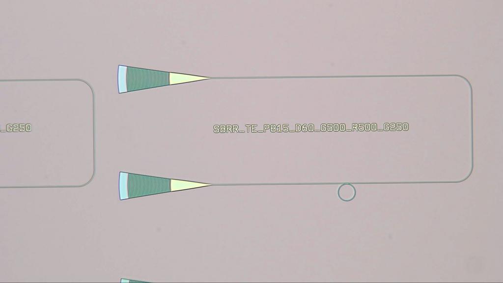
8 8 Coat, Pattern, and Develop OiR-620 Positive Photoresist Image Apply Positive Resist (300 nm) Expose Resist Develop Positive Resist Positive Resist a-si Exposed Resist a-si a-si SiO2 Silicon SiO2 Silicon SiO2 Silicon
9 9 UV Cure of OiR-620 Positive Photoresist Image UV Cure Flood Expose o 250 nm Source o 140 C o 7 min 250nm UV Light Source a-si SiO2 Silicon Hotplate
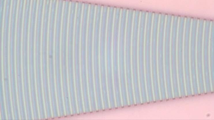
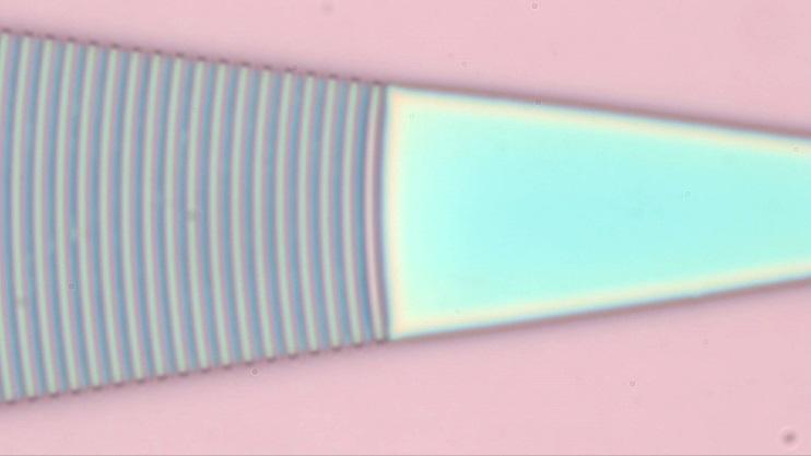
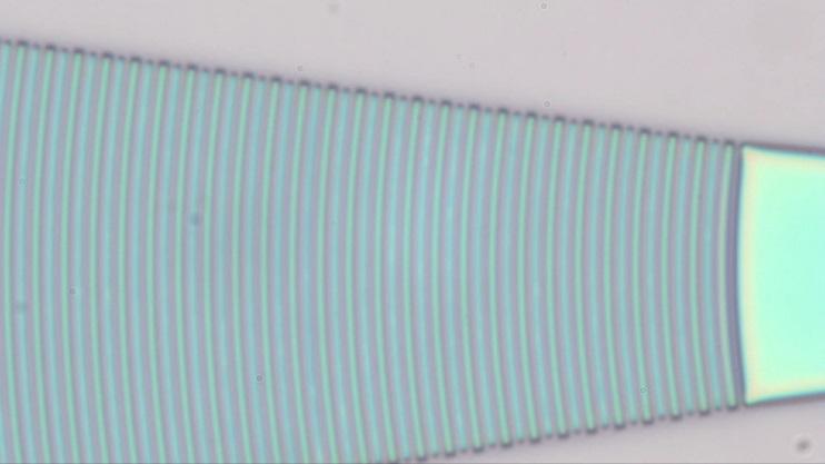
10 10 Coat, Pattern, and Develop NLOF-2020 Negative Photoresist Image Apply Negative Resist (600 nm) Expose Resist Develop Negative Resist Negative Resist a-si Unexposed Resist a-si a-si SiO2 Silicon` SiO2 Silicon SiO2 Silicon
11 RIE Etch of BARC, ICP Etch of a-si, Photoresist Strip 11 BARC Etch a-si Etch Photoresist Strip RIE Plasma ICP Plasma O 2 Plasma Ash a-si a-si a-si a-si a-si SiO2 Silicon SiO2 Silicon SiO2 Silicon
12 Final Device Profile TE Mode Waveguide nm a-si ~200 nm a-si 500 nm 2000 nm SiO2 Silicon
13 13 Process Development UV Cure DOE Impact of Exposure Time and Temperature on UV Cure Process


14 Experimental Setup 14 Study the effects of exposure time, exposure temperature, room temperature, and humidity on the area of cured photoresist remaining after processing of the second layer of photoresist Apply and develop OiR-620 photoresist without exposure UV cure the first layer Apply and develop NLOF-2020 photoresist without exposure Measure area of remaining OiR-620 photoresist SVG 88 Track UV Cure Setup
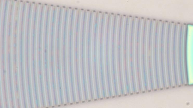
 Area (cm 2 ) Area (cm 2 ) 46.")

15 15 Design Matrix and Area of Cured Photoresist Exposure Temperature Area (cm 2 ) Area (cm 2 ) Area (cm 2 ) Exposure Time
 2.")
 Using one response variable 1.")
16 16 Method of Analysis Least Squares Regression Examined three predictor variables: 1. Exposure Temperature (Continuous) 2. Exposure Time (Continuous) 3. Humidity (Continuous) Using one response variable 1. Area of cured photoresist in cm 2 Regression Model: Area = *Time *Temp *Humidity
17 17 Process Development Engineering Design Mask


18 Design Mask Overview 18 Photonic Design Variations: 1. Ring Grating Width Duty Ratio (space:line) nm nm nm 2. Waveguide to Width Ring Gap nm nm nm 225 nm 250 nm
19 19 Experimental Results Initial Lithography Results


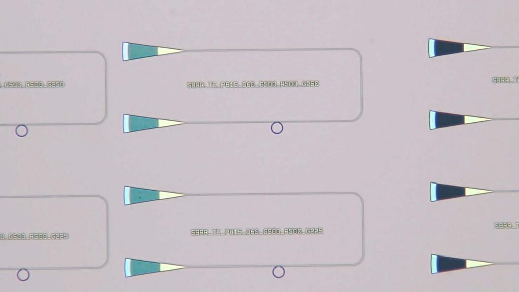
20 20 Compound Photoresist Image Positive Resist Positive Resist Negative Resist Positive Resist Negative Resist Negative Resist


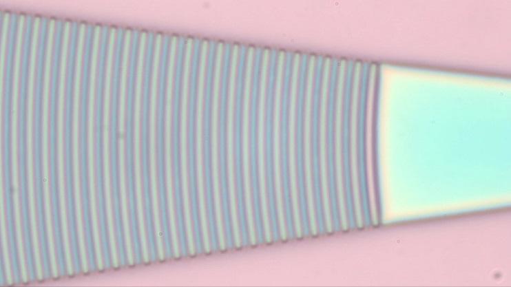
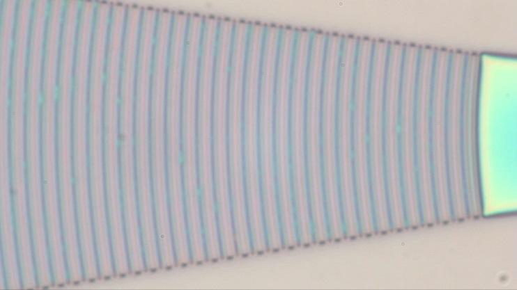
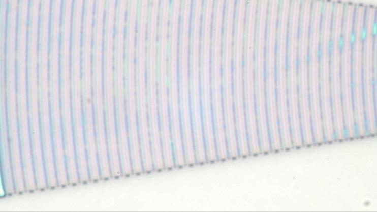
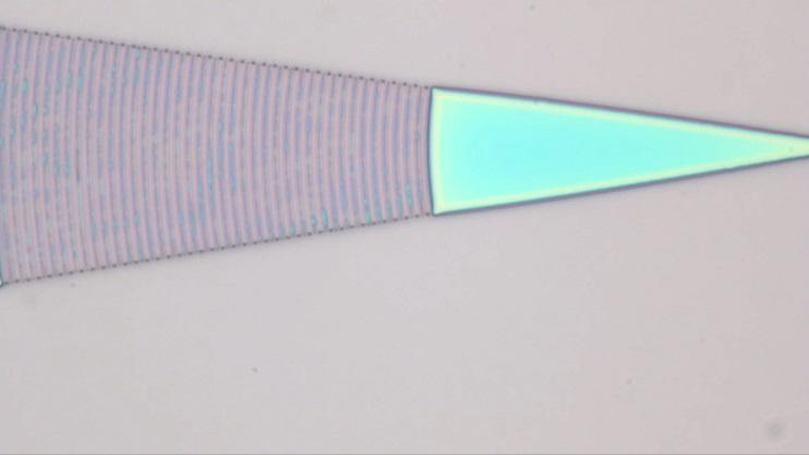
21 Affect of Pitch and Duty Ratio on Photoresist Image 21 Duty Ratio (space:line) 0.40 Pitch (nm)


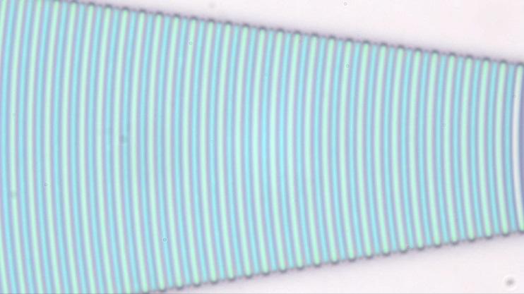
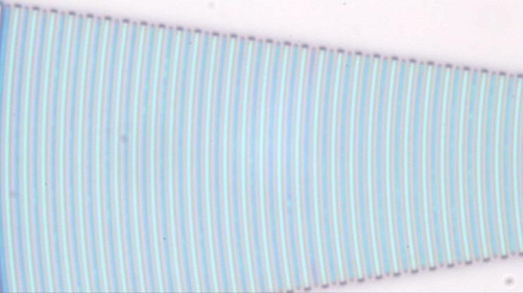
22 Affect of Pitch and Duty Ratio on Photoresist Image 22 Duty Ratio (space:line) 0.40 Pitch (nm)

23 Ring Resonator 23
24 24 Experimental Results Initial Etch Results


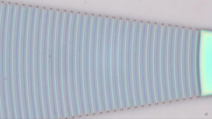
25 25 Grating Coupler Post Etch SEM nm um nm um nm nm


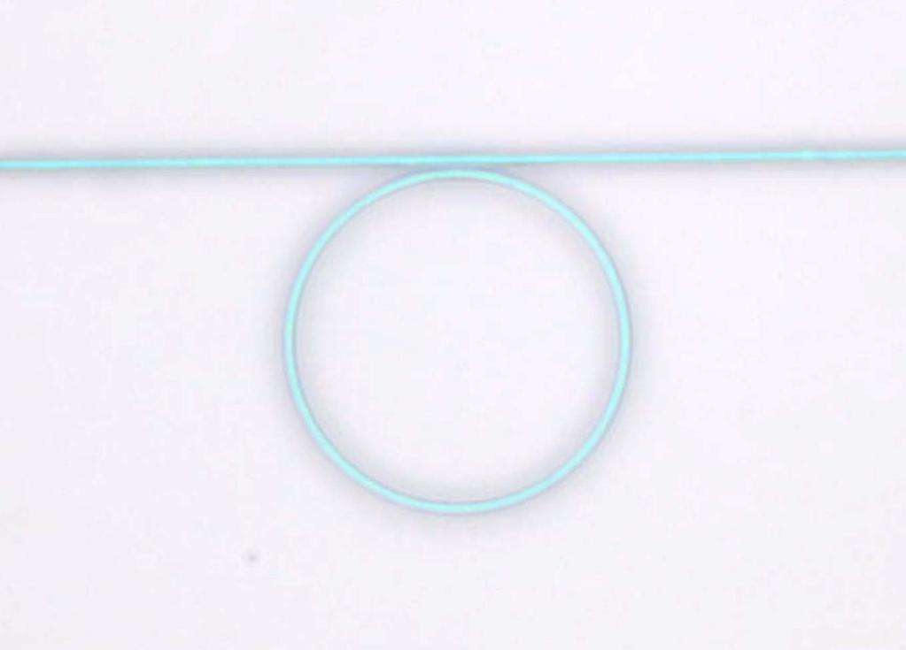
26 26 Ring Resonator Post Etch SEM nm
27 27 Conclusions Conclusions Drawn from Final Results
28 28 Conclusions Obtained successful results from experimental process: Minimum obtained feature size ~150 nm Minimum obtained feature separation - ~100 nm Developed a working UV cure process using readily obtained positive and negative tone resists Developed a working LFLE process that can be refined to fabricate working TE mode photonic devices Created a two layer engineering design mask adequate for future work
29 29 Future Work Outline of Possible Future Work
30 30 Outline of Possible Future Work Lithography optimization for SOI wafer Account for changes in stack reflectivity Separate optimization for positive and negative layers Optical Proximity Correction (OPC) mask design Corrections for bulging in ring to wave guides gap Corrections for fine pitch grating couplers Etch Recipe Optimization for compound resist image
31 31 References Works Referenced
32 Works Referenced 32 [1] S.Preble, Waveguides: Silicon Waveguides, MCEE-789/EEEE-789, Powerpoint, Spring 2165 [2] M. Maenhoudt, Alternative process schemes for double patterning that eliminate the intermediate etch step, Proc. of SPIE Vol. 6924, [3] M. Hori, et al., Sub-40nm Half-Pitch Double Patterning with Resist Freezing Process, Proc. of SPIE Vol. 6923, [4] C. Shay, CD Reduction through Annular Illumination and Sidewall Spacer Etch, Senior Design, Rochester Institute of Technology, [5] P. Cadareanu, "Silicon Photonic Devices Manufactured Using Double- Patterned iline Lithography, Rochester Institute of Technology, 2016.
Design Rules for Silicon Photonics Prototyping
 Design Rules for licon Photonics Prototyping Version 1 (released February 2008) Introduction IME s Photonics Prototyping Service offers 248nm lithography based fabrication technology for passive licon-on-insulator
DOE Project: Resist Characterization
 DOE Project: Resist Characterization GOAL To achieve high resolution and adequate throughput, a photoresist must possess relatively high contrast and sensitivity to exposing radiation. The objective of
CHAPTER 2 POLARIZATION SPLITTER- ROTATOR BASED ON A DOUBLE- ETCHED DIRECTIONAL COUPLER
 CHAPTER 2 POLARIZATION SPLITTER- ROTATOR BASED ON A DOUBLE- ETCHED DIRECTIONAL COUPLER As we discussed in chapter 1, silicon photonics has received much attention in the last decade. The main reason is
i- Line Photoresist Development: Replacement Evaluation of OiR
 i- Line Photoresist Development: Replacement Evaluation of OiR 906-12 Nishtha Bhatia High School Intern 31 July 2014 The Marvell Nanofabrication Laboratory s current i-line photoresist, OiR 897-10i, has
CMOS Digital Integrated Circuits Lec 2 Fabrication of MOSFETs
 CMOS Digital Integrated Circuits Lec 2 Fabrication of MOSFETs 1 CMOS Digital Integrated Circuits 3 rd Edition Categories of Materials Materials can be categorized into three main groups regarding their
Optolith 2D Lithography Simulator
 2D Lithography Simulator Advanced 2D Optical Lithography Simulator 4/13/05 Introduction is a powerful non-planar 2D lithography simulator that models all aspects of modern deep sub-micron lithography It
Etching Small Samples and the Effects of Using a Carrier Wafer STS ICP-RIE
 Etching Small Samples and the Effects of Using a Carrier Wafer STS ICP-RIE This note is a brief description of the effects of bonding pieces to a carrier wafer during the etch process on the STS ICP-RIE.
Holistic View of Lithography for Double Patterning. Skip Miller ASML
 Holistic View of Lithography for Double Patterning Skip Miller ASML Outline Lithography Requirements ASML Holistic Lithography Solutions Conclusions Slide 2 Shrink Continues Lithography keeps adding value
Part 5-1: Lithography
 Part 5-1: Lithography Yao-Joe Yang 1 Pattern Transfer (Patterning) Types of lithography systems: Optical X-ray electron beam writer (non-traditional, no masks) Two-dimensional pattern transfer: limited
Advanced Patterning Techniques for 22nm HP and beyond
 Advanced Patterning Techniques for 22nm HP and beyond An Overview IEEE LEOS (Bay Area) Yashesh A. Shroff Intel Corporation Aug 4 th, 2009 Outline The Challenge Advanced (optical) lithography overview Flavors
Innovative Mask Aligner Lithography for MEMS and Packaging
 Innovative Mask Aligner Lithography for MEMS and Packaging Dr. Reinhard Voelkel CEO SUSS MicroOptics SA September 9 th, 2010 1 SUSS Micro-Optics SUSS MicroOptics is a leading supplier for high-quality
Optical Lithography. Keeho Kim Nano Team / R&D DongbuAnam Semi
 Optical Lithography Keeho Kim Nano Team / R&D DongbuAnam Semi Contents Lithography = Photolithography = Optical Lithography CD : Critical Dimension Resist Pattern after Development Exposure Contents Optical
This writeup is adapted from Fall 2002, final project report for by Robert Winsor.
 Optical Waveguides in Andreas G. Andreou This writeup is adapted from Fall 2002, final project report for 520.773 by Robert Winsor. September, 2003 ABSTRACT This lab course is intended to give students
Experimental measurement of photoresist modulation curves
 Experimental measurement of photoresist modulation curves Anatoly Bourov *a,c, Stewart A. Robertson b, Bruce W. Smith c, Michael Slocum c, Emil C. Piscani c a Rochester Institute of Technology, 82 Lomb
Resist Process Window Characterization for the 45-nm Node Using an Interferometric Immersion microstepper
 Rochester Institute of Technology RIT Scholar Works Presentations and other scholarship 3-29-2006 Resist Process Window Characterization for the 45-nm Node Using an Interferometric Immersion microstepper
Lithography Simulation Tools Needed for 22nm HP and Beyond. Chris Mack
 Lithography Simulation Tools Needed for 22nm HP and Beyond Chris Mack www.lithoguru.com Slicing the Pie Simulation Tool Characteristics Precision Accuracy Capabilities (speed, features) Simulation Tool
Process Optimization
 Process Optimization Process Flow for non-critical layer optimization START Find the swing curve for the desired resist thickness. Determine the resist thickness (spin speed) from the swing curve and find
Section 2: Lithography. Jaeger Chapter 2 Litho Reader. The lithographic process
 Section 2: Lithography Jaeger Chapter 2 Litho Reader The lithographic process Photolithographic Process (a) (b) (c) (d) (e) (f) (g) Substrate covered with silicon dioxide barrier layer Positive photoresist
Section 2: Lithography. Jaeger Chapter 2 Litho Reader. EE143 Ali Javey Slide 5-1
 Section 2: Lithography Jaeger Chapter 2 Litho Reader EE143 Ali Javey Slide 5-1 The lithographic process EE143 Ali Javey Slide 5-2 Photolithographic Process (a) (b) (c) (d) (e) (f) (g) Substrate covered
Microphotonics Readiness for Commercial CMOS Manufacturing. Marco Romagnoli
 Microphotonics Readiness for Commercial CMOS Manufacturing Marco Romagnoli MicroPhotonics Consortium meeting MIT, Cambridge October 15 th, 2012 Passive optical structures based on SOI technology Building
Silicon Photonic Device Based on Bragg Grating Waveguide
 Silicon Photonic Device Based on Bragg Grating Waveguide Hwee-Gee Teo, 1 Ming-Bin Yu, 1 Guo-Qiang Lo, 1 Kazuhiro Goi, 2 Ken Sakuma, 2 Kensuke Ogawa, 2 Ning Guan, 2 and Yong-Tsong Tan 2 Silicon photonics
Key Photolithographic Outputs
 Exposure latitude Depth of Focus Exposure latitude Vs DOF plot Linearity and MEEF Isolated-Dense Bias NILS Contrast Swing Curve Reflectivity Curve 1 Exposure latitude:the range of exposure energies (usually
Optical Microlithography XXVIII
 PROCEEDINGS OF SPIE Optical Microlithography XXVIII Kafai Lai Andreas Erdmann Editors 24-26 February 2015 San Jose, California, United States Sponsored by SPIE Cosponsored by Cymer, an ASML company (United
Copyright 2000, Society of Photo-Optical Instrumentation Engineers This paper was published in Optical Microlithography XIII, Volume 4000 and is made
 Copyright 00, Society of Photo-Optical Instrumentation Engineers This paper was published in Optical Microlithography XIII, Volume 4000 and is made available as an electronic reprint with permission of
Intel's 65 nm Logic Technology Demonstrated on 0.57 µm 2 SRAM Cells
 Intel's 65 nm Logic Technology Demonstrated on 0.57 µm 2 SRAM Cells Mark Bohr Intel Senior Fellow Director of Process Architecture & Integration Intel 1 What are We Announcing? Intel has fabricated fully-functional
Feature-level Compensation & Control
 Feature-level Compensation & Control 2 Sensors and Control Nathan Cheung, Kameshwar Poolla, Costas Spanos Workshop 11/19/2003 3 Metrology, Control, and Integration Nathan Cheung, UCB SOI Wafers Multi wavelength
Section 2: Lithography. Jaeger Chapter 2. EE143 Ali Javey Slide 5-1
 Section 2: Lithography Jaeger Chapter 2 EE143 Ali Javey Slide 5-1 The lithographic process EE143 Ali Javey Slide 5-2 Photolithographic Process (a) (b) (c) (d) (e) (f) (g) Substrate covered with silicon
Index. Cambridge University Press Silicon Photonics Design Lukas Chrostowski and Michael Hochberg. Index.
 absorption, 69 active tuning, 234 alignment, 394 396 apodization, 164 applications, 7 automated optical probe station, 389 397 avalanche detector, 268 back reflection, 164 band structures, 30 bandwidth
Waveguide Bragg Gratings and Resonators LUMERICAL SOLUTIONS INC
 Waveguide Bragg Gratings and Resonators JUNE 2016 1 Outline Introduction Waveguide Bragg gratings Background Simulation challenges and solutions Photolithography simulation Initial design with FDTD Band
MICRO AND NANOPROCESSING TECHNOLOGIES
 MICRO AND NANOPROCESSING TECHNOLOGIES LECTURE 4 Optical lithography Concepts and processes Lithography systems Fundamental limitations and other issues Photoresists Photolithography process Process parameter
CHAPTER 2 Principle and Design
 CHAPTER 2 Principle and Design The binary and gray-scale microlens will be designed and fabricated. Silicon nitride and photoresist will be taken as the material of the microlens in this thesis. The design
Characterization of Photonic Structures with CST Microwave Studio. CST UGM 2010 Darmstadt
 Characterization of Photonic Structures with CST Microwave Studio Stefan Prorok, Jan Hendrik Wülbern, Jan Hampe, Hooi Sing Lee, Alexander Petrov and Manfred Eich, Institute of Optical and Electronic Materials
EUV Interference Lithography in NewSUBARU
 EUV Interference Lithography in NewSUBARU Takeo Watanabe 1, Tae Geun Kim 2, Yasuyuki Fukushima 1, Noki Sakagami 1, Teruhiko Kimura 1, Yoshito Kamaji 1, Takafumi Iguchi 1, Yuuya Yamaguchi 1, Masaki Tada
MeRck. nlof 2000 Series. technical datasheet. Negative Tone Photoresists for Single Layer Lift-Off APPLICATION TYPICAL PROCESS
 MeRck technical datasheet AZ Negative Tone Photoresists for Single Layer Lift-Off APPLICATION AZ i-line photoresists are engineered to simplify the historically complex image reversal and multilayer lift-off
Solid Immersion and Evanescent Wave Lithography at Numerical Apertures > 1.60
 Solid Immersion and Evanescent Wave Lithography at Numerical Apertures > 1.60 Bruce Smith Y. Fan, J. Zhou, L. Zavyalova, M. Slocum, J. Park, A. Bourov, E. Piscani, N. Lafferty, A. Estroff Rochester Institute
Line End Shortening. T h e L i t h o g r a p h y E x p e r t (Spring 2000) Chris A. Mack, FINLE Technologies, Austin, Texas
 Chris A. Mack, FINLE Technologies, Austin, Texas") Tutor29.doc: Version 2/15/00 Line End Shortening Chris A. Mack, FINLE Technologies, Austin, Texas T h e L i t h o g r a p h y E x p e r t (Spring 2000) Historically, lithography engineering has focused
Tutor29.doc: Version 2/15/00 Line End Shortening Chris A. Mack, FINLE Technologies, Austin, Texas T h e L i t h o g r a p h y E x p e r t (Spring 2000) Historically, lithography engineering has focused
Realization of Polarization-Insensitive Optical Polymer Waveguide Devices
 644 Realization of Polarization-Insensitive Optical Polymer Waveguide Devices Kin Seng Chiang,* Sin Yip Cheng, Hau Ping Chan, Qing Liu, Kar Pong Lor, and Chi Kin Chow Department of Electronic Engineering,
16nm with 193nm Immersion Lithography and Double Exposure
 16nm with 193nm Immersion Lithography and Double Exposure Valery Axelrad, Sequoia Design Systems, Inc. (United States) Michael C. Smayling, Tela Innovations, Inc. (United States) ABSTRACT Gridded Design
Tutor43.doc; Version 8/15/03 T h e L i t h o g r a p h y E x p e r t (November 2003)
") Tutor43.doc; Version /15/03 T h e L i t h o g r a p h y E x p e r t (November 2003) Scattering Bars Chris A. Mack, KLA-Tencor, FINLE Division, Austin, Texas Resolution enhancement technologies refer to
Tutor43.doc; Version /15/03 T h e L i t h o g r a p h y E x p e r t (November 2003) Scattering Bars Chris A. Mack, KLA-Tencor, FINLE Division, Austin, Texas Resolution enhancement technologies refer to
Major Fabrication Steps in MOS Process Flow
 Major Fabrication Steps in MOS Process Flow UV light Mask oxygen Silicon dioxide photoresist exposed photoresist oxide Silicon substrate Oxidation (Field oxide) Photoresist Coating Mask-Wafer Alignment
ECE 5745 Complex Digital ASIC Design Topic 2: CMOS Devices
 ECE 5745 Complex Digital ASIC Design Topic 2: CMOS Devices Christopher Batten School of Electrical and Computer Engineering Cornell University http://www.csl.cornell.edu/courses/ece5950 Simple Transistor
MeRck. AZ nlof technical datasheet. Negative Tone Photoresist for Single Layer Lift-Off APPLICATION TYPICAL PROCESS. SPIN CURVE (150MM Silicon)
") MeRck technical datasheet AZ nlof 5510 Negative Tone Photoresist for Single Layer Lift-Off APPLICATION AZ nlof 5510 i-line photoresist is engineered to simplify the historically complex image reversal
MeRck technical datasheet AZ nlof 5510 Negative Tone Photoresist for Single Layer Lift-Off APPLICATION AZ nlof 5510 i-line photoresist is engineered to simplify the historically complex image reversal
Evaluation of Technology Options by Lithography Simulation
 Evaluation of Technology Options by Lithography Simulation Andreas Erdmann Fraunhofer IISB, Erlangen, Germany Semicon Europe, Dresden, October 12, 2011 Outline Introduction: Resolution limits of optical
Double Exposure Using 193nm Negative Tone Photoresist
 Double Exposure Using 193nm Negative Tone Photoresist Ryoung-han Kim a, Tom Wallow a, Jongwook Kye a, Harry J. Levinson a, and Dave White b a Advanced Micro Devices, One AMD Place, Sunnyvale, CA 94088,
State-of-the-art device fabrication techniques
 State-of-the-art device fabrication techniques! Standard Photo-lithography and e-beam lithography! Advanced lithography techniques used in semiconductor industry Deposition: Thermal evaporation, e-gun
Horizontal single and multiple slot waveguides: optical transmission at λ = 1550 nm
 Horizontal single and multiple slot waveguides: optical transmission at λ = 1550 nm Rong Sun 1 *, Po Dong 2 *, Ning-ning Feng 1, Ching-yin Hong 1, Jurgen Michel 1, Michal Lipson 2, Lionel Kimerling 1 1Department
2.1 BASIC THEORY: INTERFERENCE OF TWO BEAMS
 2 LASER INTERFERENCE LITHOGRAPHY (LIL) 9 2 LASER INTERFERENCE LITHOGRAPHY (LIL) Laser interference lithography [3~22] (LIL) is a method to produce periodic structures using two interfering highly-coherent
Guided resonance reflective phase shifters
 Guided resonance reflective phase shifters Yu Horie, Amir Arbabi, and Andrei Faraon T. J. Watson Laboratory of Applied Physics, California Institute of Technology, 12 E. California Blvd., Pasadena, CA
Numerical Analysis and Optimization of a Multi-Mode Interference Polarization Beam Splitter
 Numerical Analysis and Optimization of a Multi-Mode Interference Polarization Beam Splitter Y. D Mello*, J. Skoric, M. Hui, E. Elfiky, D. Patel, D. Plant Department of Electrical Engineering, McGill University,
Superconducting Nanowire Single Photon Detector (SNSPD) integrated with optical circuits
 integrated with optical circuits") Superconducting Nanowire Single Photon Detector (SNSPD) integrated with optical circuits Marcello Graziosi, ESR 3 within PICQUE (Marie Curie ITN project) and PhD student marcello.graziosi@ifn.cnr.it Istituto
Superconducting Nanowire Single Photon Detector (SNSPD) integrated with optical circuits Marcello Graziosi, ESR 3 within PICQUE (Marie Curie ITN project) and PhD student marcello.graziosi@ifn.cnr.it Istituto
Synthesis of projection lithography for low k1 via interferometry
 Synthesis of projection lithography for low k1 via interferometry Frank Cropanese *, Anatoly Bourov, Yongfa Fan, Andrew Estroff, Lena Zavyalova, Bruce W. Smith Center for Nanolithography Research, Rochester
High Power RF MEMS Switch Technology
 High Power RF MEMS Switch Technology Invited Talk at 2005 SBMO/IEEE MTT-S International Conference on Microwave and Optoelectronics Conference Dr Jia-Sheng Hong Heriot-Watt University Edinburgh U.K. 1
OPC Rectification of Random Space Patterns in 193nm Lithography
 OPC Rectification of Random Space Patterns in 193nm Lithography Mosong Cheng, Andrew Neureuther, Keeho Kim*, Mark Ma*, Won Kim*, Maureen Hanratty* Department of Electrical Engineering and Computer Sciences
Si-EPIC Workshop: Silicon Nanophotonics Fabrication Directional Couplers
 Si-EPIC Workshop: Silicon Nanophotonics Fabrication Directional Couplers June 26, 2012 Dr. Lukas Chrostowski Directional Couplers Eigenmode solver approach Objectives Model the power coupling in a directional
Photolithography I ( Part 1 )
") 1 Photolithography I ( Part 1 ) Chapter 13 : Semiconductor Manufacturing Technology by M. Quirk & J. Serda Bjørn-Ove Fimland, Department of Electronics and Telecommunication, Norwegian University of Science
1 Photolithography I ( Part 1 ) Chapter 13 : Semiconductor Manufacturing Technology by M. Quirk & J. Serda Bjørn-Ove Fimland, Department of Electronics and Telecommunication, Norwegian University of Science
Nanophotonic Waveguides and Photonic Crystals in Silicon-on-Insulator
 Nanophotonic Waveguides and Photonic Crystals in Silicon-on-Insulator Wim Bogaerts 19 April 2004 Photonics Research Group http://photonics.intec.ugent.be nano = small photon = elementary on a scale of
Silicon nitride based TriPleX Photonic Integrated Circuits for sensing applications
 Silicon nitride based TriPleX Photonic Integrated Circuits for sensing applications Arne Leinse a.leinse@lionix-int.com 2 Our chips drive your business 2 What are Photonic ICs (PICs)? Photonic Integrated
Lecture: Integration of silicon photonics with electronics. Prepared by Jean-Marc FEDELI CEA-LETI
 Lecture: Integration of silicon photonics with electronics Prepared by Jean-Marc FEDELI CEA-LETI Context The goal is to give optical functionalities to electronics integrated circuit (EIC) The objectives
Lecture 13 Basic Photolithography
 Lecture 13 Basic Photolithography Chapter 12 Wolf and Tauber 1/64 Announcements Homework: Homework 3 is due today, please hand them in at the front. Will be returned one week from Thursday (16 th Nov).
Optical Bus for Intra and Inter-chip Optical Interconnects
 Optical Bus for Intra and Inter-chip Optical Interconnects Xiaolong Wang Omega Optics Inc., Austin, TX Ray T. Chen University of Texas at Austin, Austin, TX Outline Perspective of Optical Backplane Bus
Design of Sub-Wavelength Color Filters Design and Simulation with the RSoft Tools Synopsys, Inc. 1
 Design of Sub-Wavelength Color Filters Design and Simulation with the RSoft Tools 2018 Synopsys, Inc. 1 Outline Introduction Plasmonic color filters Dielectric color filters Related Topics Conclusion 2018
NEXT GENERATION SILICON PHOTONICS FOR COMPUTING AND COMMUNICATION PHILIPPE ABSIL
 NEXT GENERATION SILICON PHOTONICS FOR COMPUTING AND COMMUNICATION PHILIPPE ABSIL OUTLINE Introduction Platform Overview Device Library Overview What s Next? Conclusion OUTLINE Introduction Platform Overview
Supplementary information for Stretchable photonic crystal cavity with
 Supplementary information for Stretchable photonic crystal cavity with wide frequency tunability Chun L. Yu, 1,, Hyunwoo Kim, 1, Nathalie de Leon, 1,2 Ian W. Frank, 3 Jacob T. Robinson, 1,! Murray McCutcheon,
SPP waveguide sensors
 SPP waveguide sensors 1. Optical sensor - Properties - Surface plasmon resonance sensor - Long-range surface plasmon-polariton sensor 2. LR-SPP waveguide - SPP properties in a waveguide - Asymmetric double-electrode
Miniature Mid-Infrared Thermooptic Switch with Photonic Crystal Waveguide Based Silicon-on-Sapphire Mach Zehnder Interferometers
 Miniature Mid-Infrared Thermooptic Switch with Photonic Crystal Waveguide Based Silicon-on- Mach Zehnder Interferometers Yi Zou, 1,* Swapnajit Chakravarty, 2,* Chi-Jui Chung, 1 1, 2, * and Ray T. Chen
Dr. Dirk Meyners Prof. Wagner. Wagner / Meyners Micro / Nanosystems Technology
 Micro/Nanosystems Technology Dr. Dirk Meyners Prof. Wagner 1 Outline - Lithography Overview - UV-Lithography - Resolution Enhancement Techniques - Electron Beam Lithography - Patterning with Focused Ion
State-of-The-Art Dielectric Etch Technology
 State-of-The-Art Dielectric Etch Technology Koichi Yatsuda Product Marketing Manager Etch System Business Unit November 5 th, 2010 TM Outline Dielectric Etch Challenges for State-of-The-Art Devices Control
Heinrich-Hertz-Institut Berlin
 NOVEMBER 24-26, ECOLE POLYTECHNIQUE, PALAISEAU OPTICAL COUPLING OF SOI WAVEGUIDES AND III-V PHOTODETECTORS Ludwig Moerl Heinrich-Hertz-Institut Berlin Photonic Components Dept. Institute for Telecommunications,,
MICROBUMP LITHOGRAPHY FOR 3D STACKING APPLICATIONS
 MICROBUMP LITHOGRAPHY FOR 3D STACKING APPLICATIONS Patrick Jaenen, John Slabbekoorn, Andy Miller IMEC Kapeldreef 75 B-3001 Leuven, Belgium millera@imec.be Warren W. Flack, Manish Ranjan, Gareth Kenyon,
Lecture 22 Optical MEMS (4)
") EEL6935 Advanced MEMS (Spring 2005) Instructor: Dr. Huikai Xie Lecture 22 Optical MEMS (4) Agenda: Refractive Optical Elements Microlenses GRIN Lenses Microprisms Reference: S. Sinzinger and J. Jahns,
EEL6935 Advanced MEMS (Spring 2005) Instructor: Dr. Huikai Xie Lecture 22 Optical MEMS (4) Agenda: Refractive Optical Elements Microlenses GRIN Lenses Microprisms Reference: S. Sinzinger and J. Jahns,
UFNF YES Image Reversal & HMDS Oven Revision 6.0 1/22/2014 Page 1 of 5. YES Image Reversal and HMDS Oven SOP
 1/22/2014 Page 1 of 5 YES Image Reversal and HMDS Oven SOP Table of Contents 1.0 Safety 2.0 Quality Control and Calibrations 3.0 Processes Description 4.0 Process Information for Lift Off 5.0 Operation
Photoresist Absorbance and Bleaching Laboratory
 MCEE 505 Lithography Materials and Processes Page 1 of 5 Photoresist Absorbance and Bleaching Laboratory Microelectronic Engineering Rochester Institute of Technology 1. OBJECTIVE The objective of this
A process for, and optical performance of, a low cost Wire Grid Polarizer
 1.0 Introduction A process for, and optical performance of, a low cost Wire Grid Polarizer M.P.C.Watts, M. Little, E. Egan, A. Hochbaum, Chad Jones, S. Stephansen Agoura Technology Low angle shadowed deposition
Loss Reduction in Silicon Nanophotonic Waveguide Micro-bends Through Etch Profile Improvement
 Loss Reduction in Silicon Nanophotonic Waveguide Micro-bends Through Etch Profile Improvement Shankar Kumar Selvaraja, Wim Bogaerts, Dries Van Thourhout Photonic research group, Department of Information
Contact optical nanolithography using nanoscale C-shaped apertures
 Contact optical nanolithography using nanoscale C-shaped s Liang Wang, Eric X. Jin, Sreemanth M. Uppuluri, and Xianfan Xu School of Mechanical Engineering, Purdue University, West Lafayette, Indiana 47907
Mask Technology Development in Extreme-Ultraviolet Lithography
 Mask Technology Development in Extreme-Ultraviolet Lithography Anthony Yen September 6, 2013 Projected End of Optical Lithography 2013 TSMC, Ltd 1976 1979 1982 1985 1988 1991 1994 1997 2000 2003 2007 2012
Comparative Study of Binary Intensity Mask and Attenuated Phase Shift Mask using Hyper-NA Immersion Lithography for Sub-45nm Era
 Comparative Study of Binary Intensity Mask and Attenuated Phase Shift Mask using Hyper-NA Immersion Lithogr for Sub-45nm Era Tae-Seung Eom*, Jun-Taek Park, Sarohan Park, Sunyoung Koo, Jin-Soo Kim, Byoung-Hoon
Photonics and Optical Communication
 Photonics and Optical Communication (Course Number 300352) Spring 2007 Dr. Dietmar Knipp Assistant Professor of Electrical Engineering http://www.faculty.iu-bremen.de/dknipp/ 1 Photonics and Optical Communication
MICROBUMP CREATION SYSTEM FOR ADVANCED PACKAGING APPLICATIONS
 MICROBUMP CREATION SYSTEM FOR ADVANCED PACKAGING APPLICATIONS Andrew Ahr, EKC Technology, & Chester E. Balut, DuPont Electronic Technologies Alan Huffman, RTI International Abstract Today, the electronics
Super-resolution imaging through a planar silver layer
 Super-resolution imaging through a planar silver layer David O. S. Melville and Richard J. Blaikie MacDiarmid Institute for Advanced Materials and Nanotechnology, Department of Electrical and Computer
450mm and Moore s Law Advanced Packaging Challenges and the Impact of 3D
 450mm and Moore s Law Advanced Packaging Challenges and the Impact of 3D Doug Anberg VP, Technical Marketing Ultratech SOKUDO Lithography Breakfast Forum July 10, 2013 Agenda Next Generation Technology
Georgia Tech IEN EBL Facility NNIN Highlights 2014 External User Projects
 Georgia Tech IEN EBL Facility NNIN Highlights 2014 External User Projects Silicon based Photonic Crystal Devices Silicon based photonic crystal devices are ultra-small photonic devices that can confine
Figure 1 Basic waveguide structure
 Recent Progress in SOI Nanophotonic Waveguides D. Van Thourhout, P. Dumon, W. Bogaerts, G. Roelkens, D. Taillaert, G. Priem, R. Baets IMEC-Ghent University, Department of Information Technology, St. Pietersnieuwstraat
Lecture 7. Lithography and Pattern Transfer. Reading: Chapter 7
 Lecture 7 Lithography and Pattern Transfer Reading: Chapter 7 Used for Pattern transfer into oxides, metals, semiconductors. 3 types of Photoresists (PR): Lithography and Photoresists 1.) Positive: PR
Optimizing FinFET Structures with Design-based Metrology
 Lithography M e t r o l o g y Optimizing FinFET Structures with Design-based Metrology Tom Vandeweyer, Christie Delvaux, Johan De Backer, and Monique Ercken, IMEC Gian Lorusso, Radhika Jandhyala, Amir
Technology for the MEMS processing and testing environment. SUSS MicroTec AG Dr. Hans-Georg Kapitza
 Technology for the MEMS processing and testing environment SUSS MicroTec AG Dr. Hans-Georg Kapitza 1 SUSS MicroTec Industrial Group Founded 1949 as Karl Süss KG GmbH&Co. in Garching/ Munich San Jose Waterbury
450mm patterning out of darkness Backend Process Exposure Tool SOKUDO Lithography Breakfast Forum July 10, 2013 Doug Shelton Canon USA Inc.
 450mm patterning out of darkness Backend Process Exposure Tool SOKUDO Lithography Breakfast Forum 2013 July 10, 2013 Doug Shelton Canon USA Inc. Introduction Half Pitch [nm] 2013 2014 2015 2016 2017 2018
Surface Topography and Alignment Effects in UV-Modified Polyimide Films with Micron Size Patterns
 CHINESE JOURNAL OF PHYSICS VOL. 41, NO. 2 APRIL 2003 Surface Topography and Alignment Effects in UV-Modified Polyimide Films with Micron Size Patterns Ru-Pin Pan 1, Hua-Yu Chiu 1,Yea-FengLin 1,andJ.Y.Huang
Silicon Photonics Technology Platform To Advance The Development Of Optical Interconnects
 Silicon Photonics Technology Platform To Advance The Development Of Optical Interconnects By Mieke Van Bavel, science editor, imec, Belgium; Joris Van Campenhout, imec, Belgium; Wim Bogaerts, imec s associated
Radial Coupling Method for Orthogonal Concentration within Planar Micro-Optic Solar Collectors
 Radial Coupling Method for Orthogonal Concentration within Planar Micro-Optic Solar Collectors Jason H. Karp, Eric J. Tremblay and Joseph E. Ford Photonics Systems Integration Lab University of California
Silicon photonic devices based on binary blazed gratings
 Silicon photonic devices based on binary blazed gratings Zhiping Zhou Li Yu Optical Engineering 52(9), 091708 (September 2013) Silicon photonic devices based on binary blazed gratings Zhiping Zhou Li Yu
Integrated photonic circuit in silicon on insulator for Fourier domain optical coherence tomography
 Integrated photonic circuit in silicon on insulator for Fourier domain optical coherence tomography Günay Yurtsever *,a, Pieter Dumon a, Wim Bogaerts a, Roel Baets a a Ghent University IMEC, Photonics
Impact of the light coupling on the sensing properties of photonic crystal cavity modes Kumar Saurav* a,b, Nicolas Le Thomas a,b,
 Impact of the light coupling on the sensing properties of photonic crystal cavity modes Kumar Saurav* a,b, Nicolas Le Thomas a,b, a Photonics Research Group, Ghent University-imec, Technologiepark-Zwijnaarde
On-chip interrogation of a silicon-on-insulator microring resonator based ethanol vapor sensor with an arrayed waveguide grating (AWG) spectrometer
 spectrometer") On-chip interrogation of a silicon-on-insulator microring resonator based ethanol vapor sensor with an arrayed waveguide grating (AWG) spectrometer Nebiyu A. Yebo* a, Wim Bogaerts, Zeger Hens b,roel Baets
On-chip interrogation of a silicon-on-insulator microring resonator based ethanol vapor sensor with an arrayed waveguide grating (AWG) spectrometer Nebiyu A. Yebo* a, Wim Bogaerts, Zeger Hens b,roel Baets
Lithography. 3 rd. lecture: introduction. Prof. Yosi Shacham-Diamand. Fall 2004
 Lithography 3 rd lecture: introduction Prof. Yosi Shacham-Diamand Fall 2004 1 List of content Fundamental principles Characteristics parameters Exposure systems 2 Fundamental principles Aerial Image Exposure
Results of Proof-of-Concept 50keV electron multi-beam Mask Exposure Tool (emet POC)
") Results of Proof-of-Concept 50keV electron multi-beam Mask Exposure Tool (emet POC) Elmar Platzgummer *, Christof Klein, and Hans Loeschner IMS Nanofabrication AG Schreygasse 3, A-1020 Vienna, Austria
Results of Proof-of-Concept 50keV electron multi-beam Mask Exposure Tool (emet POC) Elmar Platzgummer *, Christof Klein, and Hans Loeschner IMS Nanofabrication AG Schreygasse 3, A-1020 Vienna, Austria
Quantized patterning using nanoimprinted blanks
 IOP PUBLISHING Nanotechnology 20 (2009) 155303 (7pp) Quantized patterning using nanoimprinted blanks NANOTECHNOLOGY doi:10.1088/0957-4484/20/15/155303 Stephen Y Chou 1, Wen-Di Li and Xiaogan Liang NanoStructure
Research Article Subwavelength Grating Structures in Silicon-on-Insulator Waveguides
 Advances in Optical Technologies Volume 2008, Article ID 685489, 8 pages doi:10.1155/2008/685489 Research Article Subwavelength Grating Structures in Silicon-on-Insulator Waveguides J.H.Schmid,P. Cheben,S.Janz,
MLA 150 (DLA) Presentation and examples. Théophane Besson, , Heidelberg Instruments GmbH 1
 Presentation and examples. Théophane Besson, , Heidelberg Instruments GmbH 1") MLA 150 (DLA) Presentation and examples Théophane Besson, 17.03.2015, Heidelberg Instruments GmbH 1 Presentation of the tool The MLA 150 (named DLA in the past) is a new generation Maskless Aligner developed
MLA 150 (DLA) Presentation and examples Théophane Besson, 17.03.2015, Heidelberg Instruments GmbH 1 Presentation of the tool The MLA 150 (named DLA in the past) is a new generation Maskless Aligner developed
Fabrication Techniques of Optical ICs
 Fabrication Techniques of Optical ICs Processing Techniques Lift off Process Etching Process Patterning Techniques Photo Lithography Electron Beam Lithography Photo Resist ( Microposit MP1300) Electron