Optical Lithography. Keeho Kim Nano Team / R&D DongbuAnam Semi
|
|
|
- Jared Robinson
- 6 years ago
- Views:
Transcription
1 Optical Lithography Keeho Kim Nano Team / R&D DongbuAnam Semi
2 Contents
3
4 Lithography = Photolithography = Optical Lithography CD : Critical Dimension Resist Pattern after Development Exposure
5 Contents
6 Optical Imaging System Light Aperture Illumination Lens Mask Aperture Projection Lens Wafer Source α β
7
8
9


10 Resolution Limit Result on Silicon Wafer Final Pattern after Lithography Target Layout Mask
11
12
13 Light Intensity Light Source Lens Mask Int. Intensity without Mask Photo Resist
14 Light Intensity Light Source Lens Mask Int. Intensity without Mask Under Process Just Process Over Process
15 Focus & DOF Light Source Lens Mask +Defocus Best Focus DOF -Defocus
16
17 Wavelength of Lithography System Ultraviolet F2 ArF KrF i-line h-line g-line nm : 10-9 m
18
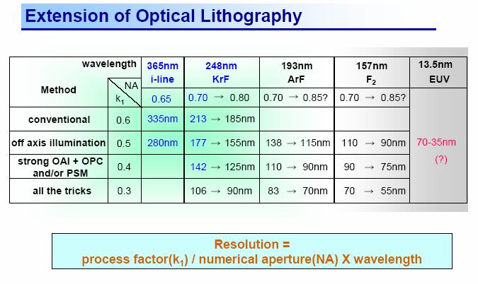
19 Optical Lithography Resolution = k 1 λ DOF = k 2 NA 2 λ NA Maximized Lithography Margin - OPC - Resolution Enhancement Technique NTI
20 Optical Lithography
21 Optical Lithography Wavelength g-line : 436nm, Hg-Xe Lamp + Optical Filter i-line : 365nm, Hg-Xe Lamp + Optical Filter DUV : 248nm, KrF Excimer Laser 193nm, ArF Excimer Laser F 2 : 157nm, F 2 Laser EUV : 13.4nm, Soft X-ray Exposure Type (Nikon, Cannon, ASML) Step and Repeat : Stepper Step and Scan : Scanner Reduction Ratio 1X(UT), 4X(Scanner), 5X(Stepper), 10X
22 Contents
23 Stepper (Step and Repeat) Light Mask Optical Lens 1/5 Light Beam Wafer Chip One Shot X Y

24 Exposure System
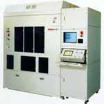
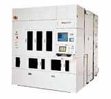
25 Optic System of Stepper (Canon)
26 Nikon Stepper Structure Reticle Light Source Wafer Projection Lens 22x22mm 2 Field
27 Nikon Scanner Slit : 8x26mm 2 Illumination System Slit 25x33mm 2 Reticle Scanning Stage Projection Lens (Slit) Wafer Scanning Stage

28 Scanner and Stepper
29 Photo Resist Resist Tone Positive : Exposed Resist (Decomposition) => Removed after Development Mask Tone == Resist Pattern Tone Negative : Exposed Resist (Cross Link) => Remains after Development Mask Tone <=> Resist Pattern Tone Mask Positive Negative
30 Photo Resist Resist Component (Sumitomo, TOK, JSR, Shin-Etsu) Sensitizer : Reaction to Light Resin : Masking to Etching Solvent : Viscosity Adjustment for Coating Thickness = Thickness(Spin Speed, Viscosity, Others) i-line Resist PAC(Photo Acid Compound) + Novolac + Solvent Exposed PAC => Decomposition => Higher Dissolution Rate DUV (KrF) Resist (Chemically Amplified Resist) PAG(Photo Acid Generator : Proton-Catalyst) + PHS + Solvent Proton Catalyze Decomposition or Cross-linking PHS => Acetal(Low Temp) / t-boc / Acrylate(High Temp)
31 In-line Process AD HP HP HP HP HP WDS WEE HP COL COL COL COL COL C/S M/A I/F COAT DEV DEV Track System Exposure System

32 Nikon Stepper & Scanner NSR-2205i14E NSR-S203B NSR-S204B

33 ASML Scanner Click Here


34 TEL Track System Mark-8 ACT-8
 PCD003 : S-9260")
35 CD-SEM System PCD001 : S-9220 (Hitachi) PCD003 : S-9260 (Hitachi)
36 Contents
37
38 Off-axis Illumination -1st Order +1st Order -1st Order +1st Order 0th Order 0th Order Conventional Off-Axis
39 Coherence Factor (σ) Effect 1 σ = 0 σ = 0~2 σ = 0 Cut Off (λ) 1/Pattern Size -1st Order 0th Order +1st Order Projection Lens (Diameter ~ NA)
40 Apertures for Off-axis Illumination σ Conventional Modified Illum. / OAI? Annular SHRINC Quadruple
41 Dipole
42 Phase Shift Mask Making Formula Shifter d OPD = = d ( n n 1 λ 2 shifter air )
43 Phase Shift Mask Mask Conventional Half Tone (4~15%) Strong PSM E-field at Mask E-field at Wafer Intensity at Wafer
44 Strong PSM Conventional Alternating (Old) Qz Cr Shifter 180 o 0 o Cr-less (Qz Etch) Alternating 0 o 180 o Shifter 180 o 0 o

45 Actual PSM Application Double Exposure Process


46 Sub Resolution Assist Features SRAF (OPC) => Process Margin Improvement
47 Pattern Type Line and Space Pattern (Pitch, Duty Ratio=Line:Space CD) Pitch CD 1:1 L/S 1:2 L/S Iso Line Iso Space
48 Pattern Type Contact Hole (Island) Pattern (Pitch, Duty Ratio=Contact CD : Spacing) Pitch CD 1:1 C/H Iso C/H Island Pattern


49 CD Linearity & Focus Margin Shin-Etsu Data


50 Actual Device Pattern Moat Design Mask Pattern (Cr / Quartz) Resist Pattern on Wafer =>


51 Actual Device Pattern Gate Design Mask Pattern (Cr / Quartz) CD Target Pattern =>


52 Mask Design / Simulation Data CD CD SEM Measurement after Development CD
53
54
55
56 Contents


57 Simulation Sequence Aerial Image Mask Latent Image Development Contours 3-D Resist Structure


58 Image Intensity => Resist Pattern Diffusion


59 Lithography Sim. Example 2-D Resist Profile 3-D Resist Profile

60 Resist Profile Cross Section
61 What s OPC? Optical Proximity Effect Correction Mask Pattern Original Pattern OPC Tool Corrected Pattern Resist Pattern
62 OPC Type Serif Jog Hammer Head Extension Scattering Bar
63 OPC at IBM
64 Contents
65
66 EUV Lithography Intel
67 SCALPEL 0.1mm Si Strut 1.1mm Membrane : SiN X ~100nm Low atomic number Scatterer : Cr/W 10nm/30nm High atomic number
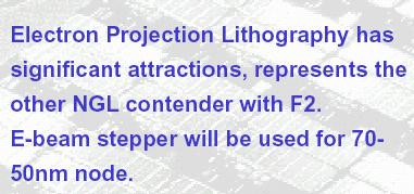
68 Electron Projection Lithography
5. Lithography. 1. photolithography intro: overall, clean room 2. principle 3. tools 4. pattern transfer 5. resolution 6. next-gen
 5. Lithography 1. photolithography intro: overall, clean room 2. principle 3. tools 4. pattern transfer 5. resolution 6. next-gen References: Semiconductor Devices: Physics and Technology. 2 nd Ed. SM
Section 2: Lithography. Jaeger Chapter 2 Litho Reader. The lithographic process
 Section 2: Lithography Jaeger Chapter 2 Litho Reader The lithographic process Photolithographic Process (a) (b) (c) (d) (e) (f) (g) Substrate covered with silicon dioxide barrier layer Positive photoresist
Section 2: Lithography. Jaeger Chapter 2 Litho Reader. EE143 Ali Javey Slide 5-1
 Section 2: Lithography Jaeger Chapter 2 Litho Reader EE143 Ali Javey Slide 5-1 The lithographic process EE143 Ali Javey Slide 5-2 Photolithographic Process (a) (b) (c) (d) (e) (f) (g) Substrate covered
Update on 193nm immersion exposure tool
 Update on 193nm immersion exposure tool S. Owa, H. Nagasaka, Y. Ishii Nikon Corporation O. Hirakawa and T. Yamamoto Tokyo Electron Kyushu Ltd. January 28, 2004 Litho Forum 1 What is immersion lithography?
Lithography. 3 rd. lecture: introduction. Prof. Yosi Shacham-Diamand. Fall 2004
 Lithography 3 rd lecture: introduction Prof. Yosi Shacham-Diamand Fall 2004 1 List of content Fundamental principles Characteristics parameters Exposure systems 2 Fundamental principles Aerial Image Exposure
Photolithography. References: Introduction to Microlithography Thompson, Willson & Bowder, 1994
 Photolithography References: Introduction to Microlithography Thompson, Willson & Bowder, 1994 Microlithography, Science and Technology Sheats & Smith, 1998 Any other Microlithography or Photolithography
Semiconductor Manufacturing Technology. Semiconductor Manufacturing Technology. Photolithography: Resist Development and Advanced Lithography
 Semiconductor Manufacturing Technology Michael Quirk & Julian Serda October 2001 by Prentice Hall Chapter 15 Photolithography: Resist Development and Advanced Lithography Eight Basic Steps of Photolithography
Section 2: Lithography. Jaeger Chapter 2. EE143 Ali Javey Slide 5-1
 Section 2: Lithography Jaeger Chapter 2 EE143 Ali Javey Slide 5-1 The lithographic process EE143 Ali Javey Slide 5-2 Photolithographic Process (a) (b) (c) (d) (e) (f) (g) Substrate covered with silicon
EE143 Fall 2016 Microfabrication Technologies. Lecture 3: Lithography Reading: Jaeger, Chap. 2
 EE143 Fall 2016 Microfabrication Technologies Lecture 3: Lithography Reading: Jaeger, Chap. 2 Prof. Ming C. Wu wu@eecs.berkeley.edu 511 Sutardja Dai Hall (SDH) 1-1 The lithographic process 1-2 1 Photolithographic
Process Optimization
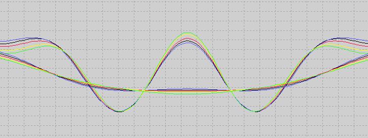
 Process Optimization Process Flow for non-critical layer optimization START Find the swing curve for the desired resist thickness. Determine the resist thickness (spin speed) from the swing curve and find
Copyright 2000, Society of Photo-Optical Instrumentation Engineers This paper was published in Optical Microlithography XIII, Volume 4000 and is made
 Copyright 00, Society of Photo-Optical Instrumentation Engineers This paper was published in Optical Microlithography XIII, Volume 4000 and is made available as an electronic reprint with permission of
Lecture 8. Microlithography
 Lecture 8 Microlithography Lithography Introduction Process Flow Wafer Exposure Systems Masks Resists State of the Art Lithography Next Generation Lithography (NGL) Recommended videos: http://www.youtube.com/user/asmlcompany#p/search/1/jh6urfqt_d4
Mask Technology Development in Extreme-Ultraviolet Lithography
 Mask Technology Development in Extreme-Ultraviolet Lithography Anthony Yen September 6, 2013 Projected End of Optical Lithography 2013 TSMC, Ltd 1976 1979 1982 1985 1988 1991 1994 1997 2000 2003 2007 2012
MICROCHIP MANUFACTURING by S. Wolf
 MICROCHIP MANUFACTURING by S. Wolf Chapter 19 LITHOGRAPHY II: IMAGE-FORMATION and OPTICAL HARDWARE 2004 by LATTICE PRESS CHAPTER 19 - CONTENTS Preliminaries: Wave- Motion & The Behavior of Light Resolution
Photolithography Technology and Application
 Photolithography Technology and Application Jeff Tsai Director, Graduate Institute of Electro-Optical Engineering Tatung University Art or Science? Lind width = 100 to 5 micron meter!! Resolution = ~ 3
Photolithography I ( Part 1 )
") 1 Photolithography I ( Part 1 ) Chapter 13 : Semiconductor Manufacturing Technology by M. Quirk & J. Serda Bjørn-Ove Fimland, Department of Electronics and Telecommunication, Norwegian University of Science
1 Photolithography I ( Part 1 ) Chapter 13 : Semiconductor Manufacturing Technology by M. Quirk & J. Serda Bjørn-Ove Fimland, Department of Electronics and Telecommunication, Norwegian University of Science
Part 5-1: Lithography
 Part 5-1: Lithography Yao-Joe Yang 1 Pattern Transfer (Patterning) Types of lithography systems: Optical X-ray electron beam writer (non-traditional, no masks) Two-dimensional pattern transfer: limited
THE CHARACTERIZATION OF CHROMELESS PHASE SHIFT MASK TECHNIQUE FOR SUB-45NM LITHOGRAPHY TAN SOON YOENG
 THE CHARACTERIZATION OF CHROMELESS PHASE SHIFT MASK TECHNIQUE FOR SUB-45NM LITHOGRAPHY TAN SOON YOENG NATIONAL UNIVERSITY OF SINGAPORE 2008 THE CHARACTERIZATION OF CHROMELESS PHASE SHIFT MASK TECHNIQUE
ECSE 6300 IC Fabrication Laboratory Lecture 3 Photolithography. Lecture Outline
 ECSE 6300 IC Fabrication Laboratory Lecture 3 Photolithography Prof. James J. Q. Lu Bldg. CII, Rooms 6229 Rensselaer Polytechnic Institute Troy, NY 12180 Tel. (518)276 2909 e mails: luj@rpi.edu http://www.ecse.rpi.edu/courses/s18/ecse
Lecture 7. Lithography and Pattern Transfer. Reading: Chapter 7
 Lecture 7 Lithography and Pattern Transfer Reading: Chapter 7 Used for Pattern transfer into oxides, metals, semiconductors. 3 types of Photoresists (PR): Lithography and Photoresists 1.) Positive: PR
MICRO AND NANOPROCESSING TECHNOLOGIES
 MICRO AND NANOPROCESSING TECHNOLOGIES LECTURE 4 Optical lithography Concepts and processes Lithography systems Fundamental limitations and other issues Photoresists Photolithography process Process parameter
Photolithography 光刻 Part I: Optics
 微纳光电子材料与器件工艺原理 Photolithography 光刻 Part I: Optics Xing Sheng 盛兴 Department of Electronic Engineering Tsinghua University xingsheng@tsinghua.edu.cn 1 Integrate Circuits Moore's law transistor number transistor
Optical Microlithography XXVIII
 PROCEEDINGS OF SPIE Optical Microlithography XXVIII Kafai Lai Andreas Erdmann Editors 24-26 February 2015 San Jose, California, United States Sponsored by SPIE Cosponsored by Cymer, an ASML company (United
Lithography. Development of High-Quality Attenuated Phase-Shift Masks
 Lithography S P E C I A L Development of High-Quality Attenuated Phase-Shift Masks by Toshihiro Ii and Masao Otaki, Toppan Printing Co., Ltd. Along with the year-by-year acceleration of semiconductor device
immersion optics Immersion Lithography with ASML HydroLith TWINSCAN System Modifications for Immersion Lithography by Bob Streefkerk
 immersion optics Immersion Lithography with ASML HydroLith by Bob Streefkerk For more than 25 years, many in the semiconductor industry have predicted the end of optical lithography. Recent developments,
Device Fabrication: Photolithography
 Device Fabrication: Photolithography 1 Objectives List the four components of the photoresist Describe the difference between +PR and PR Describe a photolithography process sequence List four alignment
Purpose: Explain the top advanced issues and concepts in
 Advanced Issues and Technology (AIT) Modules Purpose: Explain the top advanced issues and concepts in optical projection printing and electron-beam lithography. h AIT-1: LER and Chemically Amplified Resists
Optolith 2D Lithography Simulator
 2D Lithography Simulator Advanced 2D Optical Lithography Simulator 4/13/05 Introduction is a powerful non-planar 2D lithography simulator that models all aspects of modern deep sub-micron lithography It
Chapter 6. Photolithography
 Chapter 6 Photolithography 2006/4/10 1 Objectives List the four components of the photoresist Describe the difference between +PR and PR Describe a photolithography process sequence List four alignment
Tutor43.doc; Version 8/15/03 T h e L i t h o g r a p h y E x p e r t (November 2003)
") Tutor43.doc; Version /15/03 T h e L i t h o g r a p h y E x p e r t (November 2003) Scattering Bars Chris A. Mack, KLA-Tencor, FINLE Division, Austin, Texas Resolution enhancement technologies refer to
Tutor43.doc; Version /15/03 T h e L i t h o g r a p h y E x p e r t (November 2003) Scattering Bars Chris A. Mack, KLA-Tencor, FINLE Division, Austin, Texas Resolution enhancement technologies refer to
Optical Projection Printing and Modeling
 Optical Projection Printing and Modeling Overview of optical lithography, concepts, trends Basic Parameters and Effects (1-14) Resolution Depth of Focus; Proximity, MEEF, LES Image Calculation, Characterization
OPC Scatterbars or Assist Features
 OPC Scatterbars or Assist Features Main Feature The isolated main pattern now acts somewhat more like a periodic line and space pattern which has a higher quality image especially with focus when off-axis
Module 11: Photolithography. Lecture 14: Photolithography 4 (Continued)
") Module 11: Photolithography Lecture 14: Photolithography 4 (Continued) 1 In the previous lecture, we have discussed the utility of the three printing modes, and their relative advantages and disadvantages.
Module 11: Photolithography Lecture 14: Photolithography 4 (Continued) 1 In the previous lecture, we have discussed the utility of the three printing modes, and their relative advantages and disadvantages.
Holistic View of Lithography for Double Patterning. Skip Miller ASML
 Holistic View of Lithography for Double Patterning Skip Miller ASML Outline Lithography Requirements ASML Holistic Lithography Solutions Conclusions Slide 2 Shrink Continues Lithography keeps adding value
What s So Hard About Lithography?
 What s So Hard About Lithography? Chris A. Mack, www.lithoguru.com, Austin, Texas Optical lithography has been the mainstay of semiconductor patterning since the early days of integrated circuit production.
Lithography Is the Designer s Brush. Lithography is indispensible for defining locations and configurations of circuit elements/functions.
 Lithography 1 Lithography Is the Designer s Brush Lithography is indispensible for defining locations and configurations of circuit elements/functions. 2 ITRS 2007 The major challenge in litho: CD, CD
Immersion Lithography: New Opportunities for Semiconductor Manufacturing
 Immersion Lithography: New Opportunities for Semiconductor Manufacturing Tim Brunner, Dario Gil, Carlos Fonseca and Nakgeuon Seong IBM - SRDC Bob Streefkerk, Christian Wagner and Marco Stavenga ASML Outline
Advanced Patterning Techniques for 22nm HP and beyond
 Advanced Patterning Techniques for 22nm HP and beyond An Overview IEEE LEOS (Bay Area) Yashesh A. Shroff Intel Corporation Aug 4 th, 2009 Outline The Challenge Advanced (optical) lithography overview Flavors
Shooting for the 22nm Lithography Goal with the. Coat/Develop Track. SOKUDO Lithography Breakfast Forum 2010 July 14 (L1)
") Shooting for the 22nm Lithography Goal with the Coat/Develop Track SOKUDO Lithography Breakfast Forum 2010 July 14 (L1) Three (3) different exposure options for 22nm: Public External (L1) MAPPER Lithography
Shooting for the 22nm Lithography Goal with the Coat/Develop Track SOKUDO Lithography Breakfast Forum 2010 July 14 (L1) Three (3) different exposure options for 22nm: Public External (L1) MAPPER Lithography
Evaluation of Technology Options by Lithography Simulation
 Evaluation of Technology Options by Lithography Simulation Andreas Erdmann Fraunhofer IISB, Erlangen, Germany Semicon Europe, Dresden, October 12, 2011 Outline Introduction: Resolution limits of optical
Nanotechnology I+II 2006 / 07
 Nanotechnology for engineers Winter semester 2006-2007 Nanotechnology I+II 2006 / 07 Juergen Brugger & Patrik Hoffmann & Teams Course agenda (winter semester) Nanotechnology I winter semester (23.10.06-9.2.06)
Lecture 5. Optical Lithography
 Lecture 5 Optical Lithography Intro For most of microfabrication purposes the process (e.g. additive, subtractive or implantation) has to be applied selectively to particular areas of the wafer: patterning
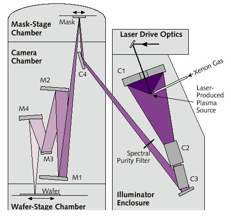
EUVL getting ready for volume introduction
 EUVL getting ready for volume introduction SEMICON West 2010 Hans Meiling, July 14, 2010 Slide 1 public Outline ASML s Lithography roadmap to support Moore s Law Progress on 0.25NA EUV systems Progress
Microlithography. exposing radiation. mask. imaging system (low pass filter) photoresist. develop. etch
 photoresist. develop. etch") Microlithography Geometry Trends Master Patterns: Mask technology Pattern Transfer: Mask Aligner technology Wafer Transfer Media: Photo resist technology mask blank: transparent, mechanically rigid masking
Microlithography Geometry Trends Master Patterns: Mask technology Pattern Transfer: Mask Aligner technology Wafer Transfer Media: Photo resist technology mask blank: transparent, mechanically rigid masking
Advanced Digital Integrated Circuits. Lecture 2: Scaling Trends. Announcements. No office hour next Monday. Extra office hour Tuesday 2-3pm
 EE241 - Spring 20 Advanced Digital Integrated Circuits Lecture 2: Scaling Trends and Features of Modern Technologies Announcements No office hour next Monday Extra office hour Tuesday 2-3pm 2 1 Outline
Optical Lithography. Here Is Why. Burn J. Lin SPIE PRESS. Bellingham, Washington USA
 Optical Lithography Here Is Why Burn J. Lin SPIE PRESS Bellingham, Washington USA Contents Preface xiii Chapter 1 Introducing Optical Lithography /1 1.1 The Role of Lithography in Integrated Circuit Fabrication
Micro- and Nano-Technology... for Optics
 Micro- and Nano-Technology...... for Optics 3.2 Lithography U.D. Zeitner Fraunhofer Institut für Angewandte Optik und Feinmechanik Jena Printing on Stones Map of Munich Stone Print Contact Printing light
Photolithography II ( Part 2 )
") 1 Photolithography II ( Part 2 ) Chapter 14 : Semiconductor Manufacturing Technology by M. Quirk & J. Serda Saroj Kumar Patra, Department of Electronics and Telecommunication, Norwegian University of Science
1 Photolithography II ( Part 2 ) Chapter 14 : Semiconductor Manufacturing Technology by M. Quirk & J. Serda Saroj Kumar Patra, Department of Electronics and Telecommunication, Norwegian University of Science
PHGN/CHEN/MLGN 435/535: Interdisciplinary Silicon Processing Laboratory. Simple Si solar Cell!
 Where were we? Simple Si solar Cell! Two Levels of Masks - photoresist, alignment Etch and oxidation to isolate thermal oxide, deposited oxide, wet etching, dry etching, isolation schemes Doping - diffusion/ion
Comparative Study of Binary Intensity Mask and Attenuated Phase Shift Mask using Hyper-NA Immersion Lithography for Sub-45nm Era
 Comparative Study of Binary Intensity Mask and Attenuated Phase Shift Mask using Hyper-NA Immersion Lithogr for Sub-45nm Era Tae-Seung Eom*, Jun-Taek Park, Sarohan Park, Sunyoung Koo, Jin-Soo Kim, Byoung-Hoon
From ArF Immersion to EUV Lithography
 From ArF Immersion to EUV Lithography Luc Van den hove Vice President IMEC Outline Introduction 193nm immersion lithography EUV lithography Global collaboration Conclusions Lithography is enabling 1000
OPC Rectification of Random Space Patterns in 193nm Lithography
 OPC Rectification of Random Space Patterns in 193nm Lithography Mosong Cheng, Andrew Neureuther, Keeho Kim*, Mark Ma*, Won Kim*, Maureen Hanratty* Department of Electrical Engineering and Computer Sciences
Synthesis of projection lithography for low k1 via interferometry
 Synthesis of projection lithography for low k1 via interferometry Frank Cropanese *, Anatoly Bourov, Yongfa Fan, Andrew Estroff, Lena Zavyalova, Bruce W. Smith Center for Nanolithography Research, Rochester
State-of-the-art device fabrication techniques
 State-of-the-art device fabrication techniques! Standard Photo-lithography and e-beam lithography! Advanced lithography techniques used in semiconductor industry Deposition: Thermal evaporation, e-gun
Purpose: Explain the top 10 phenomena and concepts. BPP-1: Resolution and Depth of Focus (1.5X)
") Basic Projection Printing (BPP) Modules Purpose: Explain the top 10 phenomena and concepts key to understanding optical projection printing BPP-1: Resolution and Depth of Focus (1.5X) BPP-2: Bragg condition
Basic Projection Printing (BPP) Modules Purpose: Explain the top 10 phenomena and concepts key to understanding optical projection printing BPP-1: Resolution and Depth of Focus (1.5X) BPP-2: Bragg condition
2009 International Workshop on EUV Lithography
 Contents Introduction Absorber Stack Optimization Non-flatness Correction Blank Defect and Its Mitigation Wafer Printing Inspection Actinic Metrology Cleaning and Repair Status Remaining Issues in EUV
Lecture 13 Basic Photolithography
 Lecture 13 Basic Photolithography Chapter 12 Wolf and Tauber 1/64 Announcements Homework: Homework 3 is due today, please hand them in at the front. Will be returned one week from Thursday (16 th Nov).
Chapter 6 Photolithography
 Chapter 6 Photolithography Hong Xiao, Ph. D. hxiao89@hotmail.com www2.austin.cc.tx.us/hongxiao/book.htm Hong Xiao, Ph. D. www2.austin.cc.tx.us/hongxiao/book.htm 1 Objectives List the four components of
Lecture 8 Chemical 4 Engineering for Micro/Nano Fabrication
 Lecture 8 Chemical 4 Engineering for Micro/Nano Fabrication 3 B 2 1 Amplitude 0 l Direction -1-2 Phase Improving -3 Resolution by Wavefront Engineering -4-20 0 20 40 60 80 100 Is this our only option???
Major Fabrication Steps in MOS Process Flow
 Major Fabrication Steps in MOS Process Flow UV light Mask oxygen Silicon dioxide photoresist exposed photoresist oxide Silicon substrate Oxidation (Field oxide) Photoresist Coating Mask-Wafer Alignment
Micro- and Nano-Technology... for Optics
 Micro- and Nano-Technology...... for Optics 3.2 Lithography U.D. Zeitner Fraunhofer Institut für Angewandte Optik und Feinmechanik Jena Printing on Stones Map of Munich Stone Print Shadow Printing Photomask
CHARACTERIZATION OF THE IMPACT OF SCATTERED LIGHT AND POWER ILLUMINATION NON UNIFORMITY ON SEMICONDUCTOR PROCESSES
 CHARACTERIZATION OF THE IMPACT OF SCATTERED LIGHT AND POWER ILLUMINATION NON UNIFORMITY ON SEMICONDUCTOR PROCESSES By Rajesh Joshi A thesis submitted in fulfillment of the requirement for the degree of
Jung Sik Kim, Seongchul Hong, Jae Uk Lee, Seung Min Lee, and Jinho Ahn*
 Jung Sik Kim, Seongchul Hong, Jae Uk Lee, Seung Min Lee, and Jinho Ahn* Photon shot noise effect in EUVL Degrades stochastic imaging performance Suggestion of a thin attenuated PSM Comparing PSM with conventional
EE-527: MicroFabrication
 EE-57: MicroFabrication Exposure and Imaging Photons white light Hg arc lamp filtered Hg arc lamp excimer laser x-rays from synchrotron Electrons Ions Exposure Sources focused electron beam direct write
Optics for EUV Lithography
 Optics for EUV Lithography Dr. Sascha Migura, Carl Zeiss SMT GmbH, Oberkochen, Germany 2018 EUVL Workshop June 13 th, 2018 Berkeley, CA, USA The resolution of the optical system determines the minimum
450mm patterning out of darkness Backend Process Exposure Tool SOKUDO Lithography Breakfast Forum July 10, 2013 Doug Shelton Canon USA Inc.
 450mm patterning out of darkness Backend Process Exposure Tool SOKUDO Lithography Breakfast Forum 2013 July 10, 2013 Doug Shelton Canon USA Inc. Introduction Half Pitch [nm] 2013 2014 2015 2016 2017 2018
Challenges of EUV masks and preliminary evaluation
 Challenges of EUV masks and preliminary evaluation Naoya Hayashi Electronic Device Laboratory Dai Nippon Printing Co.,Ltd. EUV Mask Workshop 2004 1 Contents Recent Lithography Options on Roadmap Challenges
Sub-12nm Optical Lithography with 4x Pitch Division and SMO-Lite
 Sub-12nm Optical Lithography with 4x Pitch Division and SMO-Lite Michael C. Smayling* a, Koichiro Tsujita b, Hidetami Yaegashi c, Valery Axelrad d Tadashi Arai b, Kenichi Oyama c, Arisa Hara c a Tela Innovations,
Newer process technology (since 1999) includes :
 includes :") Newer process technology (since 1999) includes : copper metalization hi-k dielectrics for gate insulators si on insulator strained silicon lo-k dielectrics for interconnects Immersion lithography for masks
Newer process technology (since 1999) includes : copper metalization hi-k dielectrics for gate insulators si on insulator strained silicon lo-k dielectrics for interconnects Immersion lithography for masks
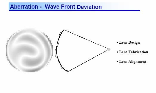
Optical Issues in Photolithography
 OpenStax-CNX module: m25448 1 Optical Issues in Photolithography Andrew R. Barron This work is produced by OpenStax-CNX and licensed under the Creative Commons Attribution License 3.0 note: This module
Photoresists & Ancillaries. Materials for Semiconductor Manufacturing A TECHCET Critical Materials Report
 2018-19 Photoresists & Ancillaries Materials for Semiconductor Manufacturing A TECHCET Critical Materials Report Prepared by Ed Korczynski Reviewed and Edited by Lita Shon-Roy TECHCET CA LLC PO Box 3814
Development of a LFLE Double Pattern Process for TE Mode Photonic Devices. Mycahya Eggleston Advisor: Dr. Stephen Preble
 Development of a LFLE Double Pattern Process for TE Mode Photonic Devices Mycahya Eggleston Advisor: Dr. Stephen Preble 2 Introduction and Motivation Silicon Photonics Geometry, TE vs TM, Double Pattern
ADVANCED TECHNOLOGY FOR EXTENDING OPTICAL LITHOGRAPHY
 ADVANCED TECHNOLOGY FOR EXTENDING OPTICAL LITHOGRAPHY Christian Wagner a, Winfried Kaiser a, Jan Mulkens b, Donis G. Flagello c a Carl Zeiss, D-73446 Oberkochen, Germany; b ASM Lithography, De Run 1110,
Module - 2 Lecture - 13 Lithography I
 Nano Structured Materials-Synthesis, Properties, Self Assembly and Applications Prof. Ashok. K.Ganguli Department of Chemistry Indian Institute of Technology, Delhi Module - 2 Lecture - 13 Lithography
Outline. 1 Introduction. 2 Basic IC fabrication processes. 3 Fabrication techniques for MEMS. 4 Applications. 5 Mechanics issues on MEMS MDL NTHU
 Outline 1 Introduction 2 Basic IC fabrication processes 3 Fabrication techniques for MEMS 4 Applications 5 Mechanics issues on MEMS 2.2 Lithography Reading: Runyan Chap. 5, or 莊達人 Chap. 7, or Wolf and
Eun-Jin Kim, GukJin Kim, Seong-Sue Kim*, Han-Ku Cho*, Jinho Ahn**, Ilsin An, and Hye-Keun Oh
 Eun-Jin Kim, GukJin Kim, Seong-Sue Kim*, Han-Ku Cho*, Jinho Ahn**, Ilsin An, and Hye-Keun Oh Lithography Lab. Department of Applied Physics, Hanyang University, Korea *Samsung Electronics Co., LTD. Korea
EUV Lithography Transition from Research to Commercialization
 EUV Lithography Transition from Research to Commercialization Charles W. Gwyn and Peter J. Silverman and Intel Corporation Photomask Japan 2003 Pacifico Yokohama, Kanagawa, Japan Gwyn:PMJ:4/17/03:1 EUV
EUVL Scanners Operational at Chipmakers. Skip Miller Semicon West 2011
 EUVL Scanners Operational at Chipmakers Skip Miller Semicon West 2011 Outline ASML s Lithography roadmap to support Moore s Law Progress on NXE:3100 (0.25NA) EUV systems Progress on NXE:3300 (0.33NA) EUV
(Complementary E-Beam Lithography)
") Extending Optical Lithography with C E B L (Complementary E-Beam Lithography) July 13, 2011 4008 Burton Drive, Santa Clara, CA 95054 Outline Complementary Lithography E-Beam Complements Optical Multibeam
Extending Optical Lithography with C E B L (Complementary E-Beam Lithography) July 13, 2011 4008 Burton Drive, Santa Clara, CA 95054 Outline Complementary Lithography E-Beam Complements Optical Multibeam
Clean Room Technology Optical Lithography. Lithography I. takenfrombdhuey
 Clean Room Technology Optical Lithography Lithography I If the automobile had followed the same development cycle as the computer, a Rolls Royce would today cost $100, get a million miles per gallon, and
Mutually Optimizing Resolution Enhancement Techniques: Illumination, APSM, Assist Feature OPC, and Gray Bars
 Mutually Optimizing Resolution Enhancement Techniques: Illumination, APSM, Assist Feature OPC, and Gray Bars Bruce W. Smith Rochester Institute of Technology, Microelectronic Engineering Department, 82
Feature-level Compensation & Control
 Feature-level Compensation & Control 2 Lithography Andrew Neureuther and Costas Spanos, UCB Workshop & Review 04/15/2004 11/19/2003 - Lithography 3 Lithography: Andy Neureuther, UCB Research Themes: Linking
Innovative Mask Aligner Lithography for MEMS and Packaging
 Innovative Mask Aligner Lithography for MEMS and Packaging Dr. Reinhard Voelkel CEO SUSS MicroOptics SA September 9 th, 2010 1 SUSS Micro-Optics SUSS MicroOptics is a leading supplier for high-quality
Lithography Roadmap. without immersion lithography. Node Half pitch. 248nm. 193nm. 157nm EUVL. 3-year cycle: 2-year cycle: imec 2005
 Lithography Roadmap without immersion lithography Node Half pitch 180 nm 130 nm 90 nm 65 nm 45 nm 32 nm 22 nm 250 nm 180 nm 130 nm 90 nm 65 nm 45 nm 32 nm 248nm 193nm 157nm EUVL 3-year cycle: 2-year cycle:
Microlithography. Dale E. Ewbank ul ppt. Microlithography Dale E. Ewbank page 1
 Dale E. Ewbank dale.ewbank@rit.edu ul012014.ppt 2014 Dale E. Ewbank page 1 OUTLINE Masks Optical Lithography Photoresist Sensitivity Processing Exposure Tools Advanced Processes page 2 MICROLITHOGRAPHY
* AIT-5: Maskless, High-NA, Immersion, EUV, Imprint
 Advanced Issues and Technology (AIT) Modules Purpose: Explain the top advanced issues and concepts in optical projection printing and electron-beam lithography. AIT-1: LER and CAR AIT-2: Resolution Enhancement
Optical Proximity Effects
 T h e L i t h o g r a p h y E x p e r t (Spring 1996) Optical Proximity Effects Chris A. Mack, FINLE Technologies, Austin, Texas Proximity effects are the variations in the linewidth of a feature (or the
Reducing Proximity Effects in Optical Lithography
 INTERFACE '96 This paper was published in the proceedings of the Olin Microlithography Seminar, Interface '96, pp. 325-336. It is made available as an electronic reprint with permission of Olin Microelectronic
NANOFABRICATION, THE NEW GENERATION OF LITHOGRAPHY. Cheng-Sheng Huang & Alvin Chang ABSTRACT
 NANOFABRICATION, THE NEW GENERATION OF LITHOGRAPHY Cheng-Sheng Huang & Alvin Chang ABSTRACT Fabrication on the micro- and nano-structure has opened the new horizons in science and engineering. The success
Nikon F2 Exposure Tool
 F2 Exposure Tool Soichi Owa, Naomasa Shiraishi, Issei Tanaka, Yasuhiro Ohmura, Toshihiko Ozawa, Teruki Kobayashi, Kazushi Nomura, Takashi Aoki, and Takayuki Mizutani Corporation NSR 157nm Data Review 1
Impact of 3-D Mask Effects on CD and Overlay over Image Field in Extreme Ultraviolet Lithography
 Impact of 3-D Mask Effects on CD and Overlay over Image Field in Extreme Ultraviolet Lithography 5 th International EUV Symposium Barcelona, Spain Sven Trogisch Markus Bender Frank-Michael Kamm Disclaimer
Photolithography Module
 Electronics Workforce Development System Photolithography Module Introduction Photolithography Module This module will teach students the different types of microlithographic systems being used today,
Requirements and designs of illuminators for microlithography
 Keynote Address Requirements and designs of illuminators for microlithography Paul Michaloski Corning Tropel Corporation Fairport, New York ABSTRACT The beam shaping by illuminators of microlithographic
Effect of Reticle CD Uniformity on Wafer CD Uniformity in the Presence of Scattering Bar Optical Proximity Correction
 Effect of Reticle CD Uniformity on Wafer CD Uniformity in the Presence of Scattering Bar Optical Proximity Correction Konstantinos Adam*, Robert Socha**, Mircea Dusa**, and Andrew Neureuther* *University
Lithography Simulation Tools Needed for 22nm HP and Beyond. Chris Mack
 Lithography Simulation Tools Needed for 22nm HP and Beyond Chris Mack www.lithoguru.com Slicing the Pie Simulation Tool Characteristics Precision Accuracy Capabilities (speed, features) Simulation Tool
Advanced Mix & Match Using a High NA i-line Scanner
 Advanced Mix & Match Using a High NA i-line Scanner Jan Pieter Kuijten, Thomas Harris, Ludo van der Heijden ASML, Veldhoven, The Netherlands David Witko, John Cossins, James Foster, Douglas Ritchie ASML,
Imaging for the next decade
 Imaging for the next decade Martin van den Brink Executive Vice President Products & Technology IMEC Technology Forum 2009 3 June, 2009 Slide 1 Congratulations! ASML and years of making chips better Slide
CONTACT HOLE IMAGING AT THE 0.13 µm NODE USING KrF LITHOGRAPHY
 CONTACT HOLE IMAGING AT THE.13 µm NODE USING KrF LITHOGRAPHY Carsten Kohler, Eelco van Setten, Jo Finders ASML, Veldhoven, The Netherlands This paper was first presented at the Arch Chemicals Seminar,
Application-Based Opportunities for Reused Fab Lines
 Application-Based Opportunities for Reused Fab Lines Semicon China, March 17 th 2010 Keith Best Simax Lithography S I M A X A L L I A N C E P A R T N E R S Outline Market: Exciting More than Moore applications
Copyright 2000 by the Society of Photo-Optical Instrumentation Engineers.
 Copyright by the Society of Photo-Optical Instrumentation Engineers. This paper was published in the proceedings of Optical Microlithography XIII, SPIE Vol. 4, pp. 658-664. It is made available as an electronic