Micro- and Nano-Technology... for Optics
|
|
|
- Gertrude Houston
- 6 years ago
- Views:
Transcription


1 Micro- and Nano-Technology for Optics 3.2 Lithography U.D. Zeitner Fraunhofer Institut für Angewandte Optik und Feinmechanik Jena

2 Printing on Stones Map of Munich Stone Print


3 Shadow Printing Photomask Wikipedia Mask Wafer Curtesy: R. Völkel, Suss Microoptics
4 Contact Printing light mask resist substrate

5 Mask Aligner

6 Mask Aligner


7 Mercury Emission Spectrum high pressure Hg-vapor lamp i h g e - line
8 Proximity Printing light mask proximity gap resist substrate

9 Pattern Generation by Photolithography Standard contact photolithography with a Mask Aligner: mask illumination photomask z diffraction pattern geometric shadow printing reduction of resolution with increasing z
10 The inverse microscope microscope lithography light source image object microscope lens object projection lens image light source
11 Projection Lithography light mask Resolution: R = k 1 λ NA projection optics resist R minimum feature size k 1 optics dependent factor wavelength NA numerical aperture of imaging system substrate


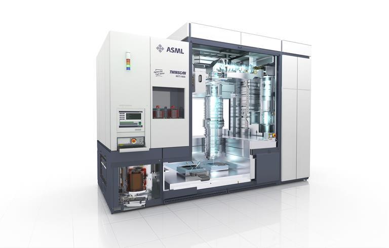
12 High-End Lithography Tool microelectronic chips on Si-wafers DUV lithography stepper, =193nm (ASML) EUV lithography stepper, =13.5nm (ASML) very low flexibility

13 resist thickness after development Photo Resist UV-exposure: Photoinitiator creates reactive species Chemical solubility in alkaline media changes Example: DNQ-based positive resist: Positive Resist: D 1 hard resist Dose D th x D log 10 D resist D 2 exposure dose D
14 Printing Result: Hard Resist Dose D th x Resist pattern: resist (almost) binary profile
15 resist thickness after development Gradation Curve D 1 hard resist suitable for binary pattern soft resist D log 10 D D 2 exposure dose D dose range for variable dose writing of continuous surface reliefs
16 Printing Result: Soft Resist Dose x Resist pattern: resist continuous surface profile (typically nonlinear wrt. exposure dose)
17 Technology for continuous profiles variable dose exposure: intensity modulated exposure beam proportional transfer (RIE): Ions (e.g. CF 4 ) resist substrate development: t 1 t 2 dose dependent profile depth in resist after development process element profile transferred into substrate material
18 Photolithography Examples
19 ASML-Stepper
20 Stepper Objective for DUV-Lithography aspheric lenses Zeiss SMT, WO 2003/075049
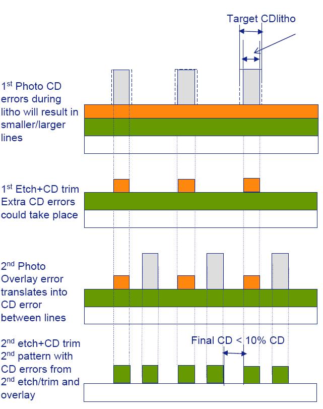
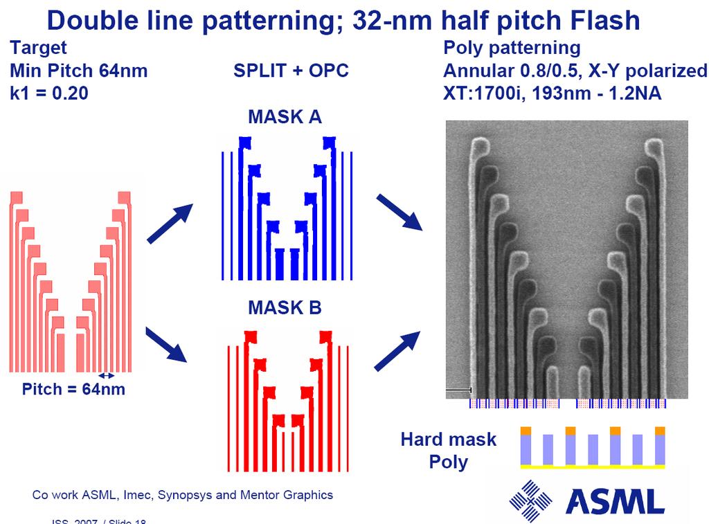
21 Double Patterning
22
")

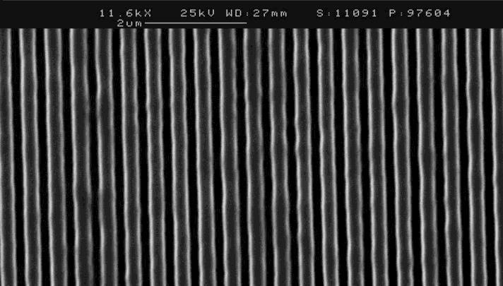
23 Pre-Compensation of Diffraction Effects Optical Proximity Correction (OPC) without OPC with OPC mask layout serifs Example: image on wafer edge rounding line shortening
24 Physics of Half-Tone- and Gray-Tone-Masks filling factor: small medium high grating period or pitch > Principle of half tone masks blocking of higher orders by a lens grating period ore pitch < brightness in the wafer plane Principle of gray tone masks higher orders do not exist - Sub wavelength masks - HEBS glass masks - LDW glass masks


25 Half-Tone Lithography type of masks pulse width pulse density Also possible: - combinations - Error diffusion half tone mask Courtesy of K. Reimer, ISIT/FhG objective gray tone image


26 Holography Example: resist structure laser beam 1 laser beam 2 resist substrate lithographic exposure with an interference pattern source: Horiba Jobin Yvon
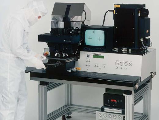
27 Holography Setup Amplitude split by beam-splitter (Ar + laser) (pinhole for spatial coherence)

28 Holography Examples single exposure two crossed exposures
29 Mask Aligner With Collimated Illumination normal incidence Suss MA6-NFH oblique incidence mercury lamp collimator polarizer interference filter cold-light mirror mask substrate special features: adjustable angle of incidence: 0deg- 55deg ( 1deg ) low divergence: 0.1deg interference filter: 313nm, 365nm, 435nm 6 7
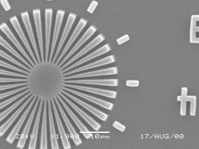
30 Principle of Pattern Transfer Mask Resist Substrate L 0 d b -1 0 th -1 st h Parameters: Wavelength / Pitch d Angle of incidence Groove depth h Duty cycle f = b / d Two beam interference only 0 th and -1 st order wavelength 2d 3 2d Symmetric diffraction angles Littrow - mounting angle of incidence sin L 2d Equal intensities rigorous calculations duty cycle and groove depth of the mask grating
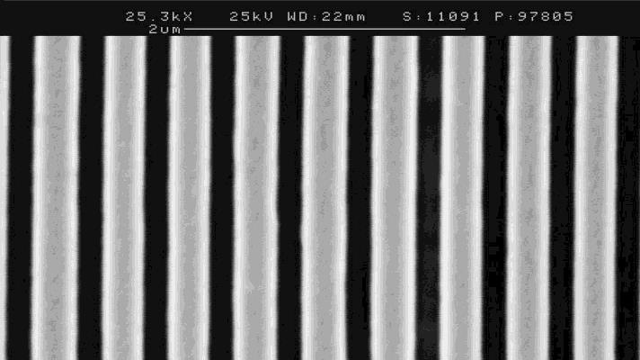
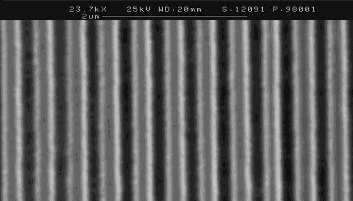
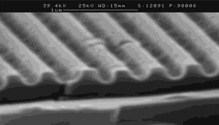
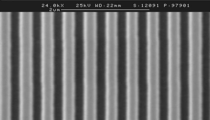
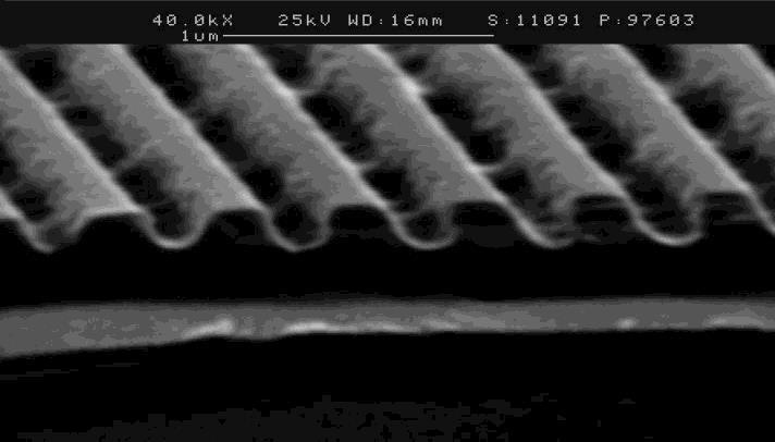
31 Experimental Results Phase mask Amplitude mask Mask 1 µm Copy 1 µm 1 µm
32 Incidence Angle p p m p p=p m /2 /2 < p < 3 /2 /2 < p < also usable for gratings with different orientations (e.g. circular gratings)
33 Laser Lithography


34 Laser Lithography Scanning Beam AOM AOD U~ profile U~ deflection angle mirror focusing lens scan width substrate motion

35 DWL 400-FF Laser Writer HIMT
36 DWL 400-FF Laser Writer basis system: Laser: max. writing field: min. spot size: autofocus system: writing mode: writing speed: DWL 400, Heidelberg Instruments =405nm (laser diode) 200mm x 200mm 1µm optical variable dose (max. 128 level) spot positioning by stage movement and beam deflection lateral scan (width up to 200µm at max. resolution) mm²/min on planar substrates (depending on structure) writing on curved substrates: substrate table: cardanic mount, tilt in two orthogonal axes min. radius of curvature: 10mm max. surface tilt angle: <10 max. sag: 30mm


37 Lithography with variable dose exposure e-beam, laser beam variable dose exposure: intensity modulated exposure beam resist substrate y writing path x substrate movement development: t 1 t 2 dose dependent profile depth after development process high flexibility for arbitrary surface profiles
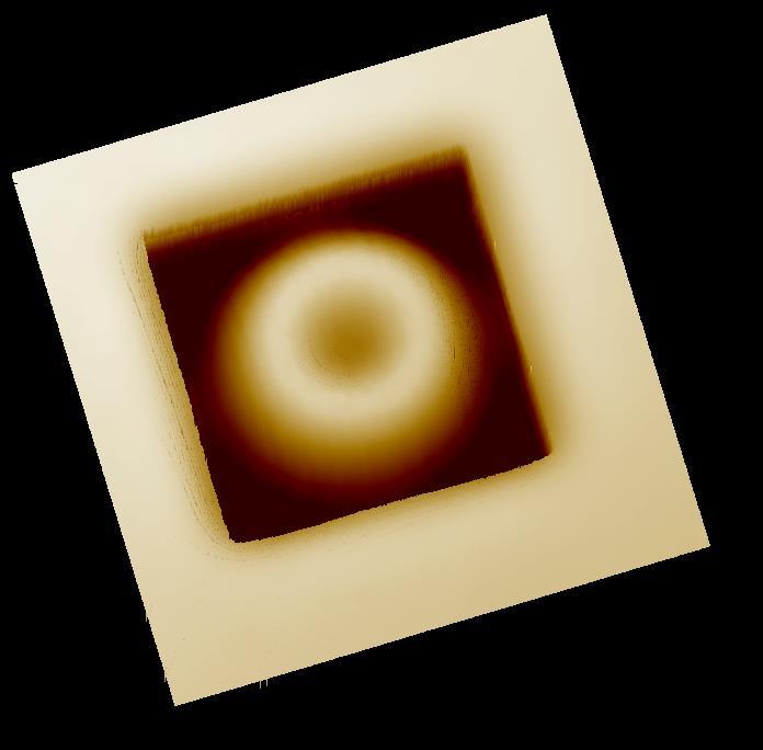
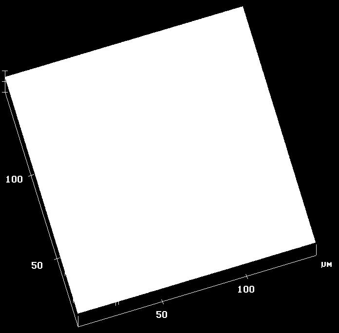

38 Laserlithography Example Structures refractive lens array profile depth: 35µm diffractive lens array profile depth: 1.5µm diffractive beam shaper profile depth: 1.2µm refractive beam shaper depth: 1.7µm refractive beam shaper profile depth: 6µm
")
39 Electron Beam Column electron gun beam on/of control magnetic deflection system and objective aperture detector stage positioning system x/y-stage Laser interferometer (position feedback)
40 Beam Diameter (Example) here: about 6nm beam size with proper systems 0.5nm beam size is achievable
41 Material Interaction Photons Electrons electron beam 20keV Dose 5-8µm (material dependent) scattering of electrons in the material distribution of deposited dose exponential absorption (Lambert-Beer) complex distribution
42 Electron Deceleration deceleration: numerous material dependent secondary effects: secondary electrons Auger-electrons characteristic x-ray radiation Bremsstrahlung radiation primary electrons resist substrate direction changes in statistical order
43 Interaction Volume primary electrons increasing beam energy resist substrate scattering volume

44 Monte-Carlo Simulation of Electron Scattering electron beam resist substrate Proximity Function
45 relative energy density Proximity Function log region 2: back scattered electrons L... total path length of an electron 0,5µm r L region 3: x-ray radiation and extensions of the beam region 1: primary electrons 0 r 0, 5µm radius r


46 Direct Exposure of a NaCl-Crystal exposure with high dose atoms are ionized and can be released from the crystal direct image of the beam pattern, realized by a fine electron beam on a NaCl crystal

47 Statistics of the Exposure Process PMMA 250µC/cm² 10nm desired structure without diffusion with diffusion of molecules
48 Statistics of the Exposure Process FEP µC/cm² 10nm desired structure without diffusion with diffusion of molecules
49 Statistics of the Exposure Process comparison of structures in the resist 10nm desired structure PMMA 250µC/cm² FEP µC/cm²

 e - /(10nm x")

nm Photoresists")

50 High resist sensitivity in EBL no more statistical independency Resist exposure dose (µc/cm²) e - /(10nm x 10nm) LER (nm) PMMA nm ZEP nm FEP (6)nm Photoresists photons/(10nm x 10nm) DUV 5,000 20,000 2nm EUV ?? DUV Photoresist PMMA ZEP 520 FEP
 schematic modeling (polymer")
 Gauss: 30 nm diffusion: 10 nm no")
51 Roughness caused by statistic electron impact experiment (resist pattern FEP 171) schematic modeling (polymer deprotection) 400nm modeling parameters dose: 0.65 e - /nm² (10 µc/cm²) Gauss: 30 nm diffusion: 10 nm no quenching, no proximity effect
: <50nm number of dose levels: 128 address grid: 1nm overlay accuracy: 12nm (mask to mean) writing strategy: variable shaped beam / cell projection")
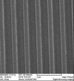
52 The Vistec SB350 OS e-beam writer basis system: SB350 OS (Optics Special), Vistec Electron Beam electron energy: 50keV max. writing field: 300mm x 300mm max. substrate thickness: 15mm resolution (direct write): <50nm number of dose levels: 128 address grid: 1nm overlay accuracy: 12nm (mask to mean) writing strategy: variable shaped beam / cell projection vector scan write-on-the-fly mode 43nm wafer resist grating 100nm period 500 nm

53 The Vistec SB350 OS e-beam writer 50keV electron column substrate loading station


54 E-beam writing strategies Gaussian beam Variable shaped beam Cell-Projection incident beam cross-section aperture angular apertures lattice aperture electron optics Gaussian spot shaped beam resolution: writing speed: >1nm low >30nm fast >30nm extreme fast


55 E-Beam Lithography: Example Structures binary grating 400nm period photonic crystal 2µm effective medium grating
![E-Beam Lithography: Variable Dose Exposure resist depth [nm] 0-200 -400-600 -800-1000 -1200-1400 -1600 fit](/docs-images/78/77153260/images/56-2.jpg "model: h = a Exp(b D) + c a = (-54.4 0.74) nm b = (0.00139 7.9E-7) cm 2 /µc c = (53 3.")

56 E-Beam Lithography: Variable Dose Exposure resist depth [nm] fit model: h = a Exp(b D) + c a = ( ) nm b = ( E-7) cm 2 /µc c = (53 3.1) nm 3µm ARP 610 exposure: 0.5A/cm 2, dose layer 1.0, 1.2, 1.5µC/cm 2 development:60s ARP-developer + 15s Isopropanol 20s ARP-developer + 15s Isopropanol measured fit blazed grating electron dose [µc/cm 2 ] diffractive element


57 Multilevel Profile Fabrication Principle: multiple executions of a binary structuring step mask 1 mask 2 mask 3 8 level profile N masks/exposures and etching steps 2 N levels
58 Expected Diffraction Efficiency (for a grating) diffraction efficiency [%] scalar theory: h sinc 2 1 N N h % % % % % number of phase levels N
![Diffraction Efficiency reduced by overlay error Efficiency normalized to ideal element [%] 100 80 60 40](/docs-images/78/77153260/images/59-1.jpg "simulation 4-level measurement 20 due to random alignment error 0-15 -10-5 0 5 10 15 20 25 30")
![misalignment normalized to pixel size [%] Alignment error in x and y normalized to pixel size [%]](/docs-images/78/77153260/images/59-2.jpg "4-level element 90% of the design efficiency 6% misalignment allowed pixel size misalignment allowed")
59 Diffraction Efficiency reduced by overlay error Efficiency normalized to ideal element [%] simulation 4-level measurement 20 due to random alignment error misalignment normalized to pixel size [%] Alignment error in x and y normalized to pixel size [%] 4-level element 90% of the design efficiency 6% misalignment allowed pixel size misalignment allowed 500nm 30nm 250nm 15nm
60 Diffraction Efficiency in Reality Diffraction efficiency expected (scalar theory) diffraction efficiency h The real diffraction efficiency depends on: - Overlay error - line width error - depth error - edge angle - design - wavelength - deflection angle - number of diffraction orders number of phase levels You will not get the best efficiency with the highest number of phase levels!!!! N

61 Micro-Lenses in Nature Water droplets Surface tension generates small droplets with ideally spherical surface shape lens


62 Resist melting technique for micro-lens fabrication resist substrate resist coating Courtesy of A. Schilling, IMT UV - light photo mask photolithography modeling of the melting development - thermal resist melting - or reflow in solvent atmosphere
63 Simplified lens design d L curvature radius of the lens: r L R h L focal length: refraction index: n f r L f ( n n ) air L d C h C h L r Ideal: diameter resist cylinder = diameter lens volume resist cylinder = volume lens L r 2 L 1 4 d 2 L resist cylinder substrate h C 1 2 h L 2 3 h d 3 L 2 L


64 NA limitation by wetting angle The rim angle R of the lens must be larger than the wetting angle W W R Typical wetting angle resist substrate ca. 25 deg dent If not: W 35 and n = 1.46 NA min 0.35 How to overcome this problem?
65 Reflow process 1) exposure resist substrate light 3) reflow solvent atmosphere pedestal 2) development 4) baking reflow technique reduces the wetting angle edge of pedestal or passivation limits the spreading Wetting angle < 1deg possible
Micro- and Nano-Technology... for Optics
 Micro- and Nano-Technology...... for Optics 3.2 Lithography U.D. Zeitner Fraunhofer Institut für Angewandte Optik und Feinmechanik Jena Printing on Stones Map of Munich Stone Print Contact Printing light
Lithography. 3 rd. lecture: introduction. Prof. Yosi Shacham-Diamand. Fall 2004
 Lithography 3 rd lecture: introduction Prof. Yosi Shacham-Diamand Fall 2004 1 List of content Fundamental principles Characteristics parameters Exposure systems 2 Fundamental principles Aerial Image Exposure
EE-527: MicroFabrication
 EE-57: MicroFabrication Exposure and Imaging Photons white light Hg arc lamp filtered Hg arc lamp excimer laser x-rays from synchrotron Electrons Ions Exposure Sources focused electron beam direct write
Major Fabrication Steps in MOS Process Flow
 Major Fabrication Steps in MOS Process Flow UV light Mask oxygen Silicon dioxide photoresist exposed photoresist oxide Silicon substrate Oxidation (Field oxide) Photoresist Coating Mask-Wafer Alignment
Part 5-1: Lithography
 Part 5-1: Lithography Yao-Joe Yang 1 Pattern Transfer (Patterning) Types of lithography systems: Optical X-ray electron beam writer (non-traditional, no masks) Two-dimensional pattern transfer: limited
Lecture 22 Optical MEMS (4)
") EEL6935 Advanced MEMS (Spring 2005) Instructor: Dr. Huikai Xie Lecture 22 Optical MEMS (4) Agenda: Refractive Optical Elements Microlenses GRIN Lenses Microprisms Reference: S. Sinzinger and J. Jahns,
EEL6935 Advanced MEMS (Spring 2005) Instructor: Dr. Huikai Xie Lecture 22 Optical MEMS (4) Agenda: Refractive Optical Elements Microlenses GRIN Lenses Microprisms Reference: S. Sinzinger and J. Jahns,
Section 2: Lithography. Jaeger Chapter 2 Litho Reader. The lithographic process
 Section 2: Lithography Jaeger Chapter 2 Litho Reader The lithographic process Photolithographic Process (a) (b) (c) (d) (e) (f) (g) Substrate covered with silicon dioxide barrier layer Positive photoresist
Section 2: Lithography. Jaeger Chapter 2 Litho Reader. EE143 Ali Javey Slide 5-1
 Section 2: Lithography Jaeger Chapter 2 Litho Reader EE143 Ali Javey Slide 5-1 The lithographic process EE143 Ali Javey Slide 5-2 Photolithographic Process (a) (b) (c) (d) (e) (f) (g) Substrate covered
Lecture 7. Lithography and Pattern Transfer. Reading: Chapter 7
 Lecture 7 Lithography and Pattern Transfer Reading: Chapter 7 Used for Pattern transfer into oxides, metals, semiconductors. 3 types of Photoresists (PR): Lithography and Photoresists 1.) Positive: PR
5. Lithography. 1. photolithography intro: overall, clean room 2. principle 3. tools 4. pattern transfer 5. resolution 6. next-gen
 5. Lithography 1. photolithography intro: overall, clean room 2. principle 3. tools 4. pattern transfer 5. resolution 6. next-gen References: Semiconductor Devices: Physics and Technology. 2 nd Ed. SM
Section 2: Lithography. Jaeger Chapter 2. EE143 Ali Javey Slide 5-1
 Section 2: Lithography Jaeger Chapter 2 EE143 Ali Javey Slide 5-1 The lithographic process EE143 Ali Javey Slide 5-2 Photolithographic Process (a) (b) (c) (d) (e) (f) (g) Substrate covered with silicon
Photolithography II ( Part 2 )
") 1 Photolithography II ( Part 2 ) Chapter 14 : Semiconductor Manufacturing Technology by M. Quirk & J. Serda Saroj Kumar Patra, Department of Electronics and Telecommunication, Norwegian University of Science
1 Photolithography II ( Part 2 ) Chapter 14 : Semiconductor Manufacturing Technology by M. Quirk & J. Serda Saroj Kumar Patra, Department of Electronics and Telecommunication, Norwegian University of Science
EE143 Fall 2016 Microfabrication Technologies. Lecture 3: Lithography Reading: Jaeger, Chap. 2
 EE143 Fall 2016 Microfabrication Technologies Lecture 3: Lithography Reading: Jaeger, Chap. 2 Prof. Ming C. Wu wu@eecs.berkeley.edu 511 Sutardja Dai Hall (SDH) 1-1 The lithographic process 1-2 1 Photolithographic
Half-tone proximity lithography
 Half-tone proximity lithography Torsten Harzendorf* a, Lorenz Stuerzebecher a, Uwe Vogler b, Uwe D. Zeitner a, Reinhard Voelkel b a Fraunhofer Institut für Angewandte Optik und Feinmechanik IOF, Albert
All-Glass Gray Scale PhotoMasks Enable New Technologies. Che-Kuang (Chuck) Wu Canyon Materials, Inc.
 Wu Canyon Materials, Inc.") All-Glass Gray Scale PhotoMasks Enable New Technologies Che-Kuang (Chuck) Wu Canyon Materials, Inc. 1 Overview All-Glass Gray Scale Photomask technologies include: HEBS-glasses and LDW-glasses HEBS-glass
All-Glass Gray Scale PhotoMasks Enable New Technologies Che-Kuang (Chuck) Wu Canyon Materials, Inc. 1 Overview All-Glass Gray Scale Photomask technologies include: HEBS-glasses and LDW-glasses HEBS-glass
Integrated Focusing Photoresist Microlenses on AlGaAs Top-Emitting VCSELs
 Integrated Focusing Photoresist Microlenses on AlGaAs Top-Emitting VCSELs Andrea Kroner We present 85 nm wavelength top-emitting vertical-cavity surface-emitting lasers (VCSELs) with integrated photoresist
Optical Waveguide Types
 8 Refractive Micro Optics Optical Waveguide Types There are two main types of optical waveguide structures: the step index and the graded index. In a step-index waveguide, the interface between the core
Optical Lithography. Keeho Kim Nano Team / R&D DongbuAnam Semi
 Optical Lithography Keeho Kim Nano Team / R&D DongbuAnam Semi Contents Lithography = Photolithography = Optical Lithography CD : Critical Dimension Resist Pattern after Development Exposure Contents Optical
Optolith 2D Lithography Simulator
 2D Lithography Simulator Advanced 2D Optical Lithography Simulator 4/13/05 Introduction is a powerful non-planar 2D lithography simulator that models all aspects of modern deep sub-micron lithography It
ECSE 6300 IC Fabrication Laboratory Lecture 3 Photolithography. Lecture Outline
 ECSE 6300 IC Fabrication Laboratory Lecture 3 Photolithography Prof. James J. Q. Lu Bldg. CII, Rooms 6229 Rensselaer Polytechnic Institute Troy, NY 12180 Tel. (518)276 2909 e mails: luj@rpi.edu http://www.ecse.rpi.edu/courses/s18/ecse
MICROCHIP MANUFACTURING by S. Wolf
 MICROCHIP MANUFACTURING by S. Wolf Chapter 19 LITHOGRAPHY II: IMAGE-FORMATION and OPTICAL HARDWARE 2004 by LATTICE PRESS CHAPTER 19 - CONTENTS Preliminaries: Wave- Motion & The Behavior of Light Resolution
EUV Plasma Source with IR Power Recycling
 1 EUV Plasma Source with IR Power Recycling Kenneth C. Johnson kjinnovation@earthlink.net 1/6/2016 (first revision) Abstract Laser power requirements for an EUV laser-produced plasma source can be reduced
MICRO AND NANOPROCESSING TECHNOLOGIES
 MICRO AND NANOPROCESSING TECHNOLOGIES LECTURE 4 Optical lithography Concepts and processes Lithography systems Fundamental limitations and other issues Photoresists Photolithography process Process parameter
Low aberration monolithic diffraction gratings for high performance optical spectrometers
 Low aberration monolithic diffraction gratings for high performance optical spectrometers Peter Triebel, Tobias Moeller, Torsten Diehl; Carl Zeiss Spectroscopy GmbH (Germany) Alexandre Gatto, Alexander
Lecture 5. Optical Lithography
 Lecture 5 Optical Lithography Intro For most of microfabrication purposes the process (e.g. additive, subtractive or implantation) has to be applied selectively to particular areas of the wafer: patterning
Project Staff: Timothy A. Savas, Michael E. Walsh, Thomas B. O'Reilly, Dr. Mark L. Schattenburg, and Professor Henry I. Smith
 9. Interference Lithography Sponsors: National Science Foundation, DMR-0210321; Dupont Agreement 12/10/99 Project Staff: Timothy A. Savas, Michael E. Walsh, Thomas B. O'Reilly, Dr. Mark L. Schattenburg,
Design Rules for Silicon Photonics Prototyping
 Design Rules for licon Photonics Prototyping Version 1 (released February 2008) Introduction IME s Photonics Prototyping Service offers 248nm lithography based fabrication technology for passive licon-on-insulator
Lecture 13 Basic Photolithography
 Lecture 13 Basic Photolithography Chapter 12 Wolf and Tauber 1/64 Announcements Homework: Homework 3 is due today, please hand them in at the front. Will be returned one week from Thursday (16 th Nov).
Computer Generated Holograms for Optical Testing
 Computer Generated Holograms for Optical Testing Dr. Jim Burge Associate Professor Optical Sciences and Astronomy University of Arizona jburge@optics.arizona.edu 520-621-8182 Computer Generated Holograms
Optical Lithography. Here Is Why. Burn J. Lin SPIE PRESS. Bellingham, Washington USA
 Optical Lithography Here Is Why Burn J. Lin SPIE PRESS Bellingham, Washington USA Contents Preface xiii Chapter 1 Introducing Optical Lithography /1 1.1 The Role of Lithography in Integrated Circuit Fabrication
Beam Shaping and Simultaneous Exposure by Diffractive Optical Element in Laser Plastic Welding
 Beam Shaping and Simultaneous Exposure by Diffractive Optical Element in Laser Plastic Welding AKL`12 9th May 2012 Dr. Daniel Vogler Page 1 Motivation: Quality and flexibility diffractive spot shaping
Photolithography. References: Introduction to Microlithography Thompson, Willson & Bowder, 1994
 Photolithography References: Introduction to Microlithography Thompson, Willson & Bowder, 1994 Microlithography, Science and Technology Sheats & Smith, 1998 Any other Microlithography or Photolithography
PHY 431 Homework Set #5 Due Nov. 20 at the start of class
 PHY 431 Homework Set #5 Due Nov. 0 at the start of class 1) Newton s rings (10%) The radius of curvature of the convex surface of a plano-convex lens is 30 cm. The lens is placed with its convex side down
Radial Coupling Method for Orthogonal Concentration within Planar Micro-Optic Solar Collectors
 Radial Coupling Method for Orthogonal Concentration within Planar Micro-Optic Solar Collectors Jason H. Karp, Eric J. Tremblay and Joseph E. Ford Photonics Systems Integration Lab University of California
CHAPTER 2 Principle and Design
 CHAPTER 2 Principle and Design The binary and gray-scale microlens will be designed and fabricated. Silicon nitride and photoresist will be taken as the material of the microlens in this thesis. The design
Innovative Mask Aligner Lithography for MEMS and Packaging
 Innovative Mask Aligner Lithography for MEMS and Packaging Dr. Reinhard Voelkel CEO SUSS MicroOptics SA September 9 th, 2010 1 SUSS Micro-Optics SUSS MicroOptics is a leading supplier for high-quality
A novel tunable diode laser using volume holographic gratings
 A novel tunable diode laser using volume holographic gratings Christophe Moser *, Lawrence Ho and Frank Havermeyer Ondax, Inc. 85 E. Duarte Road, Monrovia, CA 9116, USA ABSTRACT We have developed a self-aligned
Optical Requirements
 Optical Requirements Transmission vs. Film Thickness A pellicle needs a good light transmission and long term transmission stability. Transmission depends on the film thickness, film material and any anti-reflective
Module - 2 Lecture - 13 Lithography I
 Nano Structured Materials-Synthesis, Properties, Self Assembly and Applications Prof. Ashok. K.Ganguli Department of Chemistry Indian Institute of Technology, Delhi Module - 2 Lecture - 13 Lithography
Chapter 3 Fabrication
 Chapter 3 Fabrication The total structure of MO pick-up contains four parts: 1. A sub-micro aperture underneath the SIL The sub-micro aperture is used to limit the final spot size from 300nm to 600nm for
Photolithography I ( Part 1 )
") 1 Photolithography I ( Part 1 ) Chapter 13 : Semiconductor Manufacturing Technology by M. Quirk & J. Serda Bjørn-Ove Fimland, Department of Electronics and Telecommunication, Norwegian University of Science
1 Photolithography I ( Part 1 ) Chapter 13 : Semiconductor Manufacturing Technology by M. Quirk & J. Serda Bjørn-Ove Fimland, Department of Electronics and Telecommunication, Norwegian University of Science
Results of Proof-of-Concept 50keV electron multi-beam Mask Exposure Tool (emet POC)
") Results of Proof-of-Concept 50keV electron multi-beam Mask Exposure Tool (emet POC) Elmar Platzgummer *, Christof Klein, and Hans Loeschner IMS Nanofabrication AG Schreygasse 3, A-1020 Vienna, Austria
Results of Proof-of-Concept 50keV electron multi-beam Mask Exposure Tool (emet POC) Elmar Platzgummer *, Christof Klein, and Hans Loeschner IMS Nanofabrication AG Schreygasse 3, A-1020 Vienna, Austria
Copyright 2000 by the Society of Photo-Optical Instrumentation Engineers.
 Copyright 2000 by the Society of Photo-Optical Instrumentation Engineers. This paper was published in the proceedings of the 20 th Annual BACUS Symposium on Photomask Technology SPIE Vol. 4186, pp. 503-507.
Micro-Optic Solar Concentration and Next-Generation Prototypes
 Micro-Optic Solar Concentration and Next-Generation Prototypes Jason H. Karp, Eric J. Tremblay and Joseph E. Ford Photonics Systems Integration Lab University of California San Diego Jacobs School of Engineering
Semiconductor Manufacturing Technology. Semiconductor Manufacturing Technology. Photolithography: Resist Development and Advanced Lithography
 Semiconductor Manufacturing Technology Michael Quirk & Julian Serda October 2001 by Prentice Hall Chapter 15 Photolithography: Resist Development and Advanced Lithography Eight Basic Steps of Photolithography
NANOFABRICATION, THE NEW GENERATION OF LITHOGRAPHY. Cheng-Sheng Huang & Alvin Chang ABSTRACT
 NANOFABRICATION, THE NEW GENERATION OF LITHOGRAPHY Cheng-Sheng Huang & Alvin Chang ABSTRACT Fabrication on the micro- and nano-structure has opened the new horizons in science and engineering. The success
plasmonic nanoblock pair
 Nanostructured potential of optical trapping using a plasmonic nanoblock pair Yoshito Tanaka, Shogo Kaneda and Keiji Sasaki* Research Institute for Electronic Science, Hokkaido University, Sapporo 1-2,
Diffraction-limited performance of flat-substrate reflective imaging gratings patterned by DUV photolithography
 Diffraction-limited performance of flat-substrate reflective imaging gratings patterned by DUV photolithography Christoph M. Greiner, D. Iazikov, and T. W. Mossberg LightSmyth Technologies, 860 W Park
A process for, and optical performance of, a low cost Wire Grid Polarizer
 1.0 Introduction A process for, and optical performance of, a low cost Wire Grid Polarizer M.P.C.Watts, M. Little, E. Egan, A. Hochbaum, Chad Jones, S. Stephansen Agoura Technology Low angle shadowed deposition
Physics 431 Final Exam Examples (3:00-5:00 pm 12/16/2009) TIME ALLOTTED: 120 MINUTES Name: Signature:
 TIME ALLOTTED: 120 MINUTES Name: Signature:") Physics 431 Final Exam Examples (3:00-5:00 pm 12/16/2009) TIME ALLOTTED: 120 MINUTES Name: PID: Signature: CLOSED BOOK. TWO 8 1/2 X 11 SHEET OF NOTES (double sided is allowed), AND SCIENTIFIC POCKET CALCULATOR
Physics 431 Final Exam Examples (3:00-5:00 pm 12/16/2009) TIME ALLOTTED: 120 MINUTES Name: PID: Signature: CLOSED BOOK. TWO 8 1/2 X 11 SHEET OF NOTES (double sided is allowed), AND SCIENTIFIC POCKET CALCULATOR
Photolithography 光刻 Part I: Optics
 微纳光电子材料与器件工艺原理 Photolithography 光刻 Part I: Optics Xing Sheng 盛兴 Department of Electronic Engineering Tsinghua University xingsheng@tsinghua.edu.cn 1 Integrate Circuits Moore's law transistor number transistor
Refractive Power of a Surface. Exposure Sources. Thin Lenses. Thick Lenses. High Pressure Hg Arc Lamp Spectrum
 eractive Power o a Surace The reractive power P is measured in diopters when the radius is expressed in meters. n and n are the reractive indices o the two media. EE-57: icrofabrication n n P n n Exposure
Lecture 8. Microlithography
 Lecture 8 Microlithography Lithography Introduction Process Flow Wafer Exposure Systems Masks Resists State of the Art Lithography Next Generation Lithography (NGL) Recommended videos: http://www.youtube.com/user/asmlcompany#p/search/1/jh6urfqt_d4
Sub-50 nm period patterns with EUV interference lithography
 Microelectronic Engineering 67 68 (2003) 56 62 www.elsevier.com/ locate/ mee Sub-50 nm period patterns with EUV interference lithography * a, a a b b b H.H. Solak, C. David, J. Gobrecht, V. Golovkina,
OPTI510R: Photonics. Khanh Kieu College of Optical Sciences, University of Arizona Meinel building R.626
 OPTI510R: Photonics Khanh Kieu College of Optical Sciences, University of Arizona kkieu@optics.arizona.edu Meinel building R.626 Announcements Homework #3 is due today No class Monday, Feb 26 Pre-record
BEAM SHAPING OPTICS TO IMPROVE HOLOGRAPHIC AND INTERFEROMETRIC NANOMANUFACTURING TECHNIQUES Paper N405 ABSTRACT
 BEAM SHAPING OPTICS TO IMPROVE HOLOGRAPHIC AND INTERFEROMETRIC NANOMANUFACTURING TECHNIQUES Paper N5 Alexander Laskin, Vadim Laskin AdlOptica GmbH, Rudower Chaussee 9, 89 Berlin, Germany ABSTRACT Abstract
State-of-the-art device fabrication techniques
 State-of-the-art device fabrication techniques! Standard Photo-lithography and e-beam lithography! Advanced lithography techniques used in semiconductor industry Deposition: Thermal evaporation, e-gun
Principles of Optics for Engineers
 Principles of Optics for Engineers Uniting historically different approaches by presenting optical analyses as solutions of Maxwell s equations, this unique book enables students and practicing engineers
LOS 1 LASER OPTICS SET
 LOS 1 LASER OPTICS SET Contents 1 Introduction 3 2 Light interference 5 2.1 Light interference on a thin glass plate 6 2.2 Michelson s interferometer 7 3 Light diffraction 13 3.1 Light diffraction on a
EE119 Introduction to Optical Engineering Spring 2003 Final Exam. Name:
 EE119 Introduction to Optical Engineering Spring 2003 Final Exam Name: SID: CLOSED BOOK. THREE 8 1/2 X 11 SHEETS OF NOTES, AND SCIENTIFIC POCKET CALCULATOR PERMITTED. TIME ALLOTTED: 180 MINUTES Fundamental
Two step process for the fabrication of diffraction limited concave microlens arrays
 Two step process for the fabrication of diffraction limited concave microlens arrays Patrick Ruffieux 1*, Toralf Scharf 1, Irène Philipoussis 1, Hans Peter Herzig 1, Reinhard Voelkel 2, and Kenneth J.
Collimation Tester Instructions
 Description Use shear-plate collimation testers to examine and adjust the collimation of laser light, or to measure the wavefront curvature and divergence/convergence magnitude of large-radius optical
Synthesis of projection lithography for low k1 via interferometry
 Synthesis of projection lithography for low k1 via interferometry Frank Cropanese *, Anatoly Bourov, Yongfa Fan, Andrew Estroff, Lena Zavyalova, Bruce W. Smith Center for Nanolithography Research, Rochester
Figure 7 Dynamic range expansion of Shack- Hartmann sensor using a spatial-light modulator
 Figure 4 Advantage of having smaller focal spot on CCD with super-fine pixels: Larger focal point compromises the sensitivity, spatial resolution, and accuracy. Figure 1 Typical microlens array for Shack-Hartmann
Clean Room Technology Optical Lithography. Lithography I. takenfrombdhuey
 Clean Room Technology Optical Lithography Lithography I If the automobile had followed the same development cycle as the computer, a Rolls Royce would today cost $100, get a million miles per gallon, and
Evaluation of Technology Options by Lithography Simulation
 Evaluation of Technology Options by Lithography Simulation Andreas Erdmann Fraunhofer IISB, Erlangen, Germany Semicon Europe, Dresden, October 12, 2011 Outline Introduction: Resolution limits of optical
Confocal Imaging Through Scattering Media with a Volume Holographic Filter
 Confocal Imaging Through Scattering Media with a Volume Holographic Filter Michal Balberg +, George Barbastathis*, Sergio Fantini % and David J. Brady University of Illinois at Urbana-Champaign, Urbana,
Optical Projection Printing and Modeling
 Optical Projection Printing and Modeling Overview of optical lithography, concepts, trends Basic Parameters and Effects (1-14) Resolution Depth of Focus; Proximity, MEEF, LES Image Calculation, Characterization
membrane sample EUV characterization
 membrane sample EUV characterization Christian Laubis, PTB Outline PTB's synchrotron radiation lab Scatter from structures Scatter from random rough surfaces Measurement geometries SAXS Lifetime testing
Dr. Dirk Meyners Prof. Wagner. Wagner / Meyners Micro / Nanosystems Technology
 Micro/Nanosystems Technology Dr. Dirk Meyners Prof. Wagner 1 Outline - Lithography Overview - UV-Lithography - Resolution Enhancement Techniques - Electron Beam Lithography - Patterning with Focused Ion
Waveguiding in PMMA photonic crystals
 ROMANIAN JOURNAL OF INFORMATION SCIENCE AND TECHNOLOGY Volume 12, Number 3, 2009, 308 316 Waveguiding in PMMA photonic crystals Daniela DRAGOMAN 1, Adrian DINESCU 2, Raluca MÜLLER2, Cristian KUSKO 2, Alex.
Module 11: Photolithography. Lecture 14: Photolithography 4 (Continued)
") Module 11: Photolithography Lecture 14: Photolithography 4 (Continued) 1 In the previous lecture, we have discussed the utility of the three printing modes, and their relative advantages and disadvantages.
Module 11: Photolithography Lecture 14: Photolithography 4 (Continued) 1 In the previous lecture, we have discussed the utility of the three printing modes, and their relative advantages and disadvantages.
Chapter Ray and Wave Optics
 109 Chapter Ray and Wave Optics 1. An astronomical telescope has a large aperture to [2002] reduce spherical aberration have high resolution increase span of observation have low dispersion. 2. If two
Properties of Structured Light
 Properties of Structured Light Gaussian Beams Structured light sources using lasers as the illumination source are governed by theories of Gaussian beams. Unlike incoherent sources, coherent laser sources
Laser Speckle Reducer LSR-3000 Series
 Datasheet: LSR-3000 Series Update: 06.08.2012 Copyright 2012 Optotune Laser Speckle Reducer LSR-3000 Series Speckle noise from a laser-based system is reduced by dynamically diffusing the laser beam. A
Microlens array-based exit pupil expander for full color display applications
 Proc. SPIE, Vol. 5456, in Photon Management, Strasbourg, France, April 2004 Microlens array-based exit pupil expander for full color display applications Hakan Urey a, Karlton D. Powell b a Optical Microsystems
Use of Computer Generated Holograms for Testing Aspheric Optics
 Use of Computer Generated Holograms for Testing Aspheric Optics James H. Burge and James C. Wyant Optical Sciences Center, University of Arizona, Tucson, AZ 85721 http://www.optics.arizona.edu/jcwyant,
2.1 BASIC THEORY: INTERFERENCE OF TWO BEAMS
 2 LASER INTERFERENCE LITHOGRAPHY (LIL) 9 2 LASER INTERFERENCE LITHOGRAPHY (LIL) Laser interference lithography [3~22] (LIL) is a method to produce periodic structures using two interfering highly-coherent
Fabrication of micro structures on curve surface by X-ray lithography
 Fabrication of micro structures on curve surface by X-ray lithography Yigui Li 1, Susumu Sugiyama 2 Abstract We demonstrate experimentally the x-ray lithography techniques to fabricate micro structures
LEOK-3 Optics Experiment kit
 LEOK-3 Optics Experiment kit Physical optics, geometrical optics and fourier optics Covering 26 experiments Comprehensive documents Include experiment setups, principles and procedures Cost effective solution
Fabrication of plastic microlens array using gas-assisted micro-hot-embossing with a silicon mold
 Infrared Physics & Technology 48 (2006) 163 173 www.elsevier.com/locate/infrared Fabrication of plastic microlens array using gas-assisted micro-hot-embossing with a silicon mold C.-Y. Chang a, S.-Y. Yang
Low-cost direct writing lithography system for the sub-micron range
 Low-cost direct writing lithography system for the sub-micron range Holger Becker, Reinhard Caspary, Christian Toepfer, Manfred v. Schickfus, Siegfried Hunklinger Institut für Angewandte Physik, Universität
Imaging Systems Laboratory II. Laboratory 8: The Michelson Interferometer / Diffraction April 30 & May 02, 2002
 1051-232 Imaging Systems Laboratory II Laboratory 8: The Michelson Interferometer / Diffraction April 30 & May 02, 2002 Abstract. In the last lab, you saw that coherent light from two different locations
Exercise 8: Interference and diffraction
 Physics 223 Name: Exercise 8: Interference and diffraction 1. In a two-slit Young s interference experiment, the aperture (the mask with the two slits) to screen distance is 2.0 m, and a red light of wavelength
PHGN/CHEN/MLGN 435/535: Interdisciplinary Silicon Processing Laboratory. Simple Si solar Cell!
 Where were we? Simple Si solar Cell! Two Levels of Masks - photoresist, alignment Etch and oxidation to isolate thermal oxide, deposited oxide, wet etching, dry etching, isolation schemes Doping - diffusion/ion
SUPPLEMENTARY INFORMATION
 Optically reconfigurable metasurfaces and photonic devices based on phase change materials S1: Schematic diagram of the experimental setup. A Ti-Sapphire femtosecond laser (Coherent Chameleon Vision S)
COMPARISON OF ULTIMATE RESOLUTION ACHIEVED BY E-BEAM WRITERS WITH SHAPED BEAM AND WITH GAUSSIAN BEAM
 COMPARISON OF ULTIMATE RESOLUTION ACHIEVED BY E-BEAM WRITERS WITH SHAPED BEAM AND WITH GAUSSIAN BEAM Stanislav KRÁTKÝ a, Vladimír KOLAŘÍK a, Milan MATĚJKA a, Michal URBÁNEK a, Miroslav HORÁČEK a, Jana
Testing Aspheric Lenses: New Approaches
 Nasrin Ghanbari OPTI 521 - Synopsis of a published Paper November 5, 2012 Testing Aspheric Lenses: New Approaches by W. Osten, B. D orband, E. Garbusi, Ch. Pruss, and L. Seifert Published in 2010 Introduction
EUV Interference Lithography in NewSUBARU
 EUV Interference Lithography in NewSUBARU Takeo Watanabe 1, Tae Geun Kim 2, Yasuyuki Fukushima 1, Noki Sakagami 1, Teruhiko Kimura 1, Yoshito Kamaji 1, Takafumi Iguchi 1, Yuuya Yamaguchi 1, Masaki Tada
Tolerancing microlenses using ZEMAX
 Tolerancing microlenses using ZEMAX Andrew Stockham, John G. Smith MEMS Optical *, Inc., 05 Import Circle, Huntsville, AL, USA 35806 ABSTRACT This paper demonstrates a new tolerancing technique that allows
Optical Microlithography XXVIII
 PROCEEDINGS OF SPIE Optical Microlithography XXVIII Kafai Lai Andreas Erdmann Editors 24-26 February 2015 San Jose, California, United States Sponsored by SPIE Cosponsored by Cymer, an ASML company (United
Quantized patterning using nanoimprinted blanks
 IOP PUBLISHING Nanotechnology 20 (2009) 155303 (7pp) Quantized patterning using nanoimprinted blanks NANOTECHNOLOGY doi:10.1088/0957-4484/20/15/155303 Stephen Y Chou 1, Wen-Di Li and Xiaogan Liang NanoStructure
PICO MASTER 200. UV direct laser writer for maskless lithography
 PICO MASTER 200 UV direct laser writer for maskless lithography 4PICO B.V. Jan Tinbergenstraat 4b 5491 DC Sint-Oedenrode The Netherlands Tel: +31 413 490708 WWW.4PICO.NL 1. Introduction The PicoMaster
Be aware that there is no universal notation for the various quantities.
 Fourier Optics v2.4 Ray tracing is limited in its ability to describe optics because it ignores the wave properties of light. Diffraction is needed to explain image spatial resolution and contrast and
3.Photolithography and resist systems
 3.Photolithography and resist systems Exposure Mercury arc lamp Shadow printing projection printing Photomask Substrates Resist systems DNQ-Novolak-based Epoxy-based Polyimide based 1 Exposure Mercury
EE119 Introduction to Optical Engineering Fall 2009 Final Exam. Name:
 EE119 Introduction to Optical Engineering Fall 2009 Final Exam Name: SID: CLOSED BOOK. THREE 8 1/2 X 11 SHEETS OF NOTES, AND SCIENTIFIC POCKET CALCULATOR PERMITTED. TIME ALLOTTED: 180 MINUTES Fundamental
Electron Beam Lithography. Adam Ramm
 Electron Beam Lithography Adam Ramm Why use electrons? Negligible diffraction limitations: R = k λ NA With current optical technology, this equates to about 45nm resolution. For an electron, wavelength
Design Description Document
 UNIVERSITY OF ROCHESTER Design Description Document Flat Output Backlit Strobe Dare Bodington, Changchen Chen, Nick Cirucci Customer: Engineers: Advisor committee: Sydor Instruments Dare Bodington, Changchen
Purpose: Explain the top 10 phenomena and concepts. BPP-1: Resolution and Depth of Focus (1.5X)
") Basic Projection Printing (BPP) Modules Purpose: Explain the top 10 phenomena and concepts key to understanding optical projection printing BPP-1: Resolution and Depth of Focus (1.5X) BPP-2: Bragg condition
Basic Projection Printing (BPP) Modules Purpose: Explain the top 10 phenomena and concepts key to understanding optical projection printing BPP-1: Resolution and Depth of Focus (1.5X) BPP-2: Bragg condition
Will contain image distance after raytrace Will contain image height after raytrace
 Name: LASR 51 Final Exam May 29, 2002 Answer all questions. Module numbers are for guidance, some material is from class handouts. Exam ends at 8:20 pm. Ynu Raytracing The first questions refer to the