200mm and 300mm Test Patterned Wafers for Bonding Process Applications SKW ASSOCIATES, INC.
|
|
|
- Bonnie Casey
- 6 years ago
- Views:
Transcription
1 C M P C h a r a c t e r I z a t I o n S o l u t I o n s 200mm and 300mm Test Patterned Wafers for Bonding Process Applications SKW ASSOCIATES, INC Scott Blvd., Santa Clara, CA Tel: , Fax: SKW Associates, Inc.

2 SKW Associates, Inc, 2920 Scott Blvd. Santa Clara, CA Phone (408) Fax (408) http// SKWB-200-Ti-ND Wafer Specifications DATE: September 16, 2010 Ti 500A Silicon Ti 500A Cross Sectional View SKWB-200-Ti-ND Mask Floor Plan Patterning Center Die X Location Center Die Y Location Die Size: X Die Size: Y Die Stepping (X /Y) PARAMETER NOMINAL mm mm 1 / 1 mm TOLERANCE +/- 100 µm +/- 100 µm +/- 10 µm +/- 10 µm +/- 10% Wafers must be patterned all the way to the edges of the wafer, i.e. no area anywhere on the wafer unpatterned. (Under certain stepper operating conditions, 2 mm edge edge exclusion is allowed.)
3 PARAMETER Line CD Variation (measured on 10 µm structure) Within-Die (measured on 9 trenches) PVD Ti film thickness Within-Die NOMINAL 10 µm 500 Å TOLERANCE Si substrate: p-type (100), resistivity ohm-cm, double-side polished
4 SKW Associates, Inc, 2920 Scott Blvd. Santa Clara, CA Phone (408) Fax (408) http// SKWB-200-Ti Wafer Specifications (for defect characterization) DATE: September 16, µm 4 mm 500 µm 500 µm 4 mm 2 mm 10L/10S 10L/10S 2 mm 2 mm 20L/20S 40L/40S 20L/20S 40L/40S Ti 500A 1000A SiO2 Silicon Ti 500A 2 mm 20/20C 20/20C Cross Sectional View 500 µm SKWB3 logo SKWB-200-Ti Mask Floor Plan Patterning Center Die X Location Center Die Y Location Die Size: X Die Size: Y Die Stepping (X /Y) PARAMETER NOMINAL mm mm 1 / 1 mm TOLERANCE +/- 100 µm +/- 100 µm +/- 10 µm +/- 10 µm +/- 10% Wafers must be patterned all the way to the edges of the wafer, i.e. no area anywhere on the wafer unpatterned. (Under certain stepper operating conditions, 2 mm edge edge exclusion is allowed.)
5 PARAMETER Line CD Variation (measured on 10 µm structure) Within-Die (measured on 9 trenches) Pad Oxide thickness Within-Die PVD Ti film thickness Within-Die NOMINAL 10 µm 1000 Å 500 Å TOLERANCE +/- 3 % +/- 3 % Si substrate: p-type (100), resistivity ohm-cm, double-side polished
6 SKW Associates, Inc, 2920 Scott Blvd. Santa Clara, CA Phone (408) Fax (408) http// SKWBS-200 Wafer Specifications DATE: September 16, 2010 Cu Seed 1000A Ti 250A Oxide 500A 1 µm ECP Cu + Anneal Cu Seed 1000A Ti 250A Oxide 500A Silicon Cross Sectional View SKWBS-200 Mask Floor Plan (Additional planarization process (such as Cu CMP, etc.) will be performed upon customer s request) Patterning Center Die X Location Center Die Y Location Die Size: X Die Size: Y Die Stepping (X /Y) PARAMETER NOMINAL mm mm 1 / 1 mm TOLERANCE +/- 100 µm +/- 100 µm +/- 10 µm +/- 10 µm +/- 10% Wafers must be patterned all the way to the edges of the wafer, i.e. no area anywhere on the wafer unpatterned. (Under certain stepper operating conditions, 2 mm edge edge exclusion is allowed.)
7 PARAMETER Line CD Variation (measured on 10 µm structure) Within-Die (measured on 9 trenches) TEOS Oxide film thickness Within-Die PVD Ti film thickness Within-Die PVD Cu film thickness Within-Die ECD Cu film thickness Within-Die NOMINAL 10 µm 500 Å 250 Å 1000 Å 1 µm TOLERANCE +/- 3 % +/- 3 % Si substrate: p-type (100), resistivity ohm-cm, double-side polished
8 SKW Associates, Inc, 2920 Scott Blvd. Santa Clara, CA Phone (408) Fax (408) http// SKWB-200 Wafer Specifications (for defect characterization) DATE: September 16, µm 4 mm 500 µm 500 µm 4 mm 2 mm 2 mm 2 mm 10L/10S 20L/20S 40L/40S 10L/10S 20L/20S 40L/40S Cu Seed 1000A Ti 250A Oxide 500A 1 µm ECP Cu + Anneal Cu Seed 1000A Ti 250A Oxide 500A 500A SiN 1000A Oxide Silicon 2 mm 500 µm SKWB3 logo 20/20C 20/20C SKWB-200 Mask Floor Plan Cross Sectional View Additional planarization process (such as Cu CMP, etc.) will be performed upon customer s request) Patterning Center Die X Location Center Die Y Location Die Size: X Die Size: Y Die Stepping (X /Y) PARAMETER NOMINAL mm mm 1 / 1 mm TOLERANCE +/- 100 µm +/- 100 µm +/- 10 µm +/- 10 µm +/- 10% Wafers must be patterned all the way to the edges of the wafer, i.e. no area anywhere on the wafer unpatterned. (Under certain stepper operating conditions, 2 mm edge edge exclusion is allowed.)
9 PARAMETER Line CD Variation (measured on 10 µm structure) Within-Die (measured on 9 trenches) Pad Oxide thickness Within-Die SiN film thickness Within-Die TEOS Oxide film thickness Within-Die PVD Ti film thickness Within-Die NOMINAL 10 µm 1000 Å 500 Å 500 Å 250 Å TOLERANCE +/- 3 % +/- 3 % +/- 3 % +/- 3 %
10 PARAMETER NOMINAL PVD Cu film thickness 1000 Å Within-Die ECD Cu film thickness 1 µm Within-Die Si substrate: p-type (100), resistivity ohm-cm, double-side polished TOLERANCE
11 SKW Associates, Inc, 2920 Scott Blvd. Santa Clara, CA Phone (408) Fax (408) http// SKWB-300-Ti-ND Wafer Specifications DATE: September 16, 2010 Ti 500A Silicon Ti 500A Cross Sectional View SKWB-300-Ti-ND Mask Floor Plan Patterning Center Die X Location Center Die Y Location Die Size: X Die Size: Y Die Stepping (X /Y) PARAMETER NOMINAL mm mm 1 / 1 mm TOLERANCE +/- 100 µm +/- 100 µm +/- 10 µm +/- 10 µm +/- 10% Wafers must be patterned all the way to the edges of the wafer, i.e. no area anywhere on the wafer unpatterned. (Under certain stepper operating conditions, 4 mm edge edge exclusion is allowed.)
12 PARAMETER Line CD Variation (measured on 10 µm structure) Within-Die (measured on 9 trenches) PVD Ti film thickness Within-Die NOMINAL 10 µm 500 Å TOLERANCE Si substrate: p-type (100), resistivity ohm-cm, double-side polished
13 SKW Associates, Inc, 2920 Scott Blvd. Santa Clara, CA Phone (408) Fax (408) http// SKWB-300-Ti Wafer Specifications (for defect characterization) DATE: September 16, µm 4 mm 500 µm 500 µm 4 mm 2 mm 10L/10S 10L/10S 2 mm 2 mm 20L/20S 40L/40S 20L/20S 40L/40S Ti 500A 1000A SiO2 Silicon Ti 500A 2 mm 20/20C 20/20C Cross Sectional View 500 µm SKWB3 logo SKWB-300-Ti Mask Floor Plan Patterning Center Die X Location Center Die Y Location Die Size: X Die Size: Y Die Stepping (X /Y) PARAMETER NOMINAL mm mm 1 / 1 mm TOLERANCE +/- 100 µm +/- 100 µm +/- 10 µm +/- 10 µm +/- 10% Wafers must be patterned all the way to the edges of the wafer, i.e. no area anywhere on the wafer unpatterned. (Under certain stepper operating conditions, 4 mm edge edge exclusion is allowed.)
14 PARAMETER Line CD Variation (measured on 10 µm structure) Within-Die (measured on 9 trenches) Pad Oxide thickness Within-Die PVD Ti film thickness Within-Die NOMINAL 10 µm 1000 Å 500 Å TOLERANCE +/- 3 % +/- 3 % Si substrate: p-type (100), resistivity ohm-cm, double-side polished
15 SKW Associates, Inc, 2920 Scott Blvd. Santa Clara, CA Phone (408) Fax (408) http// SKWBS-300 Wafer Specifications DATE: September 16, 2010 Cu Seed 1000A Ti 250A Oxide 500A 1 µm ECP Cu + Anneal Cu Seed 1000A Ti 250A Oxide 500A Silicon Cross Sectional View SKWBS-300 Mask Floor Plan (Additional planarization process (such as Cu CMP, etc.) will be performed upon customer s request) Patterning Center Die X Location Center Die Y Location Die Size: X Die Size: Y Die Stepping (X /Y) PARAMETER NOMINAL mm mm 1 / 1 mm TOLERANCE +/- 100 µm +/- 100 µm +/- 10 µm +/- 10 µm +/- 10% Wafers must be patterned all the way to the edges of the wafer, i.e. no area anywhere on the wafer unpatterned. (Under certain stepper operating conditions, 4 mm edge edge exclusion is allowed.)
16 PARAMETER Line CD Variation (measured on 10 µm structure) Within-Die (measured on 9 trenches) TEOS Oxide film thickness Within-Die PVD Ti film thickness Within-Die PVD Cu film thickness Within-Die ECD Cu film thickness Within-Die NOMINAL 10 µm 500 Å 250 Å 1000 Å 1 µm TOLERANCE +/- 3 % +/- 3 % Si substrate: p-type (100), resistivity ohm-cm, double-side polished
17 SKW Associates, Inc, 2920 Scott Blvd. Santa Clara, CA Phone (408) Fax (408) http// SKWB-300 Wafer Specifications (for defect characterization) DATE: September 16, µm 4 mm 500 µm 500 µm 4 mm 2 mm 2 mm 2 mm 10L/10S 20L/20S 40L/40S 10L/10S 20L/20S 40L/40S Cu Seed 1000A Ti 250A Oxide 500A 1 µm ECP Cu + Anneal Cu Seed 1000A Ti 250A Oxide 500A 500A SiN 1000A Oxide Silicon 2 mm 500 µm SKWB3 logo 20/20C 20/20C SKWB-300 Mask Floor Plan Cross Sectional View Additional planarization process (such as Cu CMP, etc.) will be performed upon customer s request) Patterning Center Die X Location Center Die Y Location Die Size: X Die Size: Y Die Stepping (X /Y) PARAMETER NOMINAL mm mm 1 / 1 mm TOLERANCE +/- 100 µm +/- 100 µm +/- 10 µm +/- 10 µm +/- 10% Wafers must be patterned all the way to the edges of the wafer, i.e. no area anywhere on the wafer unpatterned. (Under certain stepper operating conditions, 4 mm edge edge exclusion is allowed.)
18 PARAMETER Line CD Variation (measured on 10 µm structure) Within-Die (measured on 9 trenches) Pad Oxide thickness Within-Die SiN film thickness Within-Die TEOS Oxide film thickness Within-Die PVD Ti film thickness Within-Die NOMINAL 10 µm 1000 Å 500 Å 500 Å 250 Å TOLERANCE +/- 3 % +/- 3 % +/- 3 % +/- 3 %
19 PARAMETER NOMINAL PVD Cu film thickness 1000 Å Within-Die ECD Cu film thickness 1 µm Within-Die Si substrate: p-type (100), resistivity ohm-cm, double-side polished TOLERANCE

20 SEMATECH Workshop on 3D Interconnect Metrology Standardized Test Wafers for 3D-IC Wafer Bonding Applications James Hermanowski
21 Overview Key Performance Metrics for 3D-IC Wafer Level Bonding SUSS Standardized Test Wafer Integration into 300mm Cluster Hardware and Software for Tool Self Diagnostics and Performance Metrology Metrology for Lights Out Manufacturing Test Data and Results Metrology Challenges Present and Future Summary
22 Key Performance Metrics GOAL to quickly measure and quantify interfaces created by 3D processing for process and equipment qualification Alignment drive minimum via size, electrical resistance Post bond alignment In-situ or in process metrology Measurement wafer face to wafer face, wafer face to wafer back Bond Quality voiding and micro-voiding die yield Bond Strength die yield, die lifetime Shear strength to resist damage during wafer thinning after bond Pull strength to resist mechanical, thermal or packaging stresses Hermiticity die lifetime Penetration of moisture or various undesired molecules Ability to resist degradation or deterioration Protective or seal rings around a die to prevent attack during later processing Electrical Performance yield and resistance


23 SUSS Standardized Test Wafer Design Key Features of Test Wafers Produced on various wafer types with various materials Si with Cu, Si with oxide, Si with Ti, glass with metal 300mm, 200mm, 150mm and smaller wafer sizes Mirrored design across die and wafer folds onto itself to accommodate wafer bonding 25 different machine readable targets for automated alignment testing Crosses, boxes, grids, dots, Cognex Positive and negative tone Face to Face targets, IR targets, Back to Front targets Human readable targets/verniers Quick check capability Not all companies have quick access to automation for metrology Hermeticity testing features Seven different seal rings with widths 10 microns and higher Via patterns for bond strength testing, capable of electrical testing
24 Cell Layout SUSS logo Mirrored line 0.5mm Streets 25 individual target designs Seal rings Large solid bonded area Area bonded by vias


25 Wafer Layout Cu on Si Mirrored line IR Image of Cu patterned test wafer
26 Combined Machine and Human Readable Targets Combined Target and Vernier, 0.5um
27 Vernier Examples Center Verniers: ±10micron with 1micron resolution; ±5micron with 0.25micron resolution; ±1micron with 0.1micron resolution Line length: 10, 50, 100, 200, 500, 800 (from left to right) Line length: 10, 50, 100, 200, 500, 800 (from right to left)
28 Typical Registration Verniers, 0.1 μm First Level Second Level
29 Reading Verniers In the sample shown below the long bar in the center is the zero point. The point where the red lines overlap exactly with those of the first level, black, defines the measurement. In this case the registration is found at the long central bar which happens to be zero, ie., perfect. If there was mis-registration of +0.4 μm then the forth set of bars to the right of the longer central bar would be perfectly aligned.
30 Verniers, 0.5 μm steps First Level Second Level


31 Machine Readable Marks ID Mask Model Wafer Model
32 Metrology by Linewidth Measurement Typically a box within a box type image. First Level Second Level After Alignment A x B x Registration (X-axis) = (A x B x ) /2 Resolution of features are limited by diffraction, especially when using IR

33 Metrology by Pattern Localization Dimensions In-Plane image after bonding Pattern recognition system locates origin of target #1 and target #2 Registration = Δ Origin (1, 2)
34 Example of Non-Overlapping Targets 9 μ 33.2 μ 35 μ 33.2 μ 117 μ 10 µ 10 µ Wafer #1 Wafer #2

35 Cognex Recommended Mark


36 IR Alignment Considerations Backside polished wafers: Good contrast and easy alignment Backside unpolished Difficult Metrology Heavily doped wafer Very low IR Transmission Very Difficult Metrology

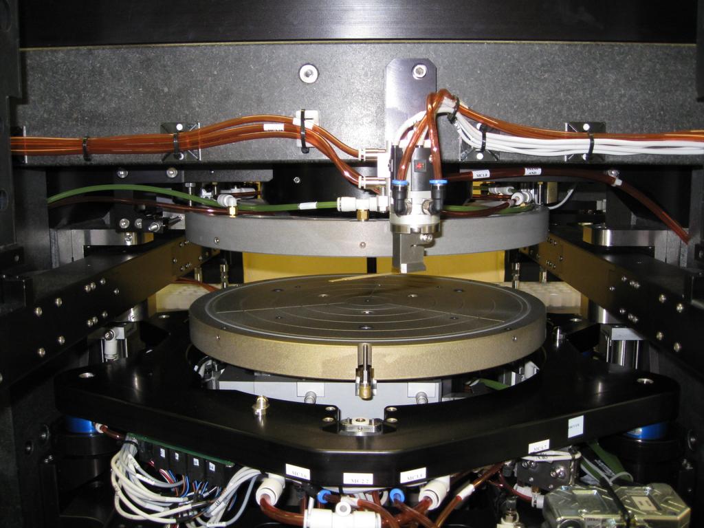
37 Integration into 300mm Production Cluster Test wafers are integrated into SUSS 300mm tooling Global Calibration Device GCD use is integrated into software for tool self characterization, calibration, or test purposes.


38 Ceramic Tooling / Fixture (Patent Pending) Supports Industry Leading Submicron Post Bond Alignment Accuracy Transports aligned pair from BA300 to CB300 Delivers reproducible submicron alignment capabilities Maintains wafer to wafer alignment throughout all process and transfer steps No exclusion zone required for clamping No cutouts in chuck for maximum yield Maintains alignment accuracy through temperature ramp Chuck CTE matches Si CTE Increases throughput by reduction of thermal mass


39 Built-in Global Calibration Global calibration runs a complete bond align cycle Measures the entire process, not just sub-systems Uses the same optics/image processing to calibrate and align Results are fed back to the system for compensation Three different alignment cycle calibration data are stored: Fixture, Fusion, RPP Global Calibration Procedure uses fixture and GCS Wafers Load calibration device/wafers Run alignment cycle Join wafers (Fixture, Fusion, RPP) Re-measure wafer alignment of joined wafers Feedback data to control system Reference = global calibration standard for XYZθ Encompasses correction for all tool movements in XYZ and theta


40 BA300UHP Bond Aligner Module High Density TSV Manufacturing Path to ±350nm post bond alignment accuracy Allows smaller via diameters and higher via densities Alignment accuracy exceeds TSV Roadmap Global calibration system accounts for all errors and motions in the system Closed loop, real time feedback Microscope tracking and correction Stage axis tracking and correction Face to Face alignments Real time with live images, not historical images Allows tooling with zero cutouts for clamps or optical paths RPP - Radial Pressure Propagation system allows engineering control over bond front during direct bonding
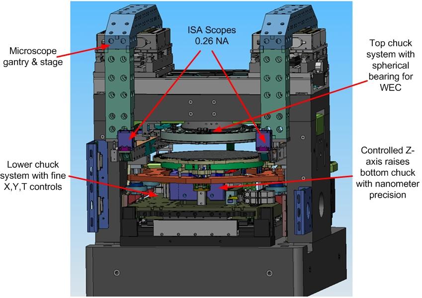
41 BA300 Components
42 BA300 Components


 0.350 0.")
 0.100 0.")
43 Fusion Aligned Wafer Results BA300 LEFT SIDE RIGHT SIDE Left - X Right - X Right - Y Left - Y Post Anneal Alignment Accuracy Wfr Pr1 Wfr Pr2 Lx (um) Ly (um) Rx (um) Ry (um)

44 BA300 Alignment Plot w/ Auto-Metrology


45 Cu-Cu Test Sequence Submicron Post Bond Alignment SUSS 300mm Cu Patterned Wafers 100KN Bond Force 425C Bond Temperature


46 Metrology for Lights Out Manufacturing IR images collected from pre-bond and post bond metrology Lights Out operation A tool monitors its own results and takes corrective action to maximize yield Pre-Bond metrology measures the alignment on wafer pairs BEFORE transfer to permanent bonding Recipe defined alignment spec and actions PASS move wafers to bonder FAIL separate and realign FAIL manual intervention FAIL reject wafers Post Bond measures the final result Recipe defined alignment spec and actions PASS tool continues operation FAIL alarm triggers user intervention to prevent more wafers from bonding Available optionally depending upon wafer and equipment configuration

47 Metrology Gage Study Micron Metrology Repeatability Left X Left Y Right X Right Y Run # Worst case example of metrology Bonded wafer pairs measured repeatedly, one reading each day Mixed target style used Wafer 1 visible target Wafer 2 IR target Stage motion required to focus on each target Illumination type changed for each target Ideal case is when both targets are: In the same plane Visible using the same illumination No need to move stages or refocus
48 Hermiticity Evaluation High resolution SAM image taken after wafer bonding Blue areas show good bond results Green areas at wafer edge show water penetration into die
49 Hermiticity Evaluation High resolution SAM image taken after additional 48 hours of water soaking Blue areas show good bond results Green areas at wafer edge show water penetration into die Water penetrates deeper into compromised die at wafer edge

50 Water Penetration of Edge Die High resolution SAM with zoom into edge die region Six die with seal rings Smallest seal ring width penetrated by water

51 Water Penetration of Edge Die 48 hour exposure to water High resolution SAM with zoom into edge die region Six die with seal rings Two seal rings penetrated by water No other rings penetrated
52 Metrology Challenges Present and Future Measurement standards for 3D alignments Wafer face aligned to wafer back via last approach and via after bonding Wafer back aligned to wafer back Interface measurements through non-transparent wafers Bond quality and alignments IR absorbing layers, metal layers and heavily doped Silicon Targets are on two different planes 3D spatially. May require visible & IR illumination How to measure when traditional forms of radiation (visible or IR) will not penetrate the wafer stack? Acoustic waves? Electrical?
53 Summary An approach to quickly measure and quantify interfaces created by 3D processing has been established for process and equipment qualification The approach uses standardized test wafers which contain features to simply and easily quantify processes and equipment used in the manufacture of 3D-IC Alignment drive minimum via size, electrical resistance Bond Quality voiding and micro-voiding die yield Bond Strength die yield, die lifetime Hermiticity die lifetime Technology has been integrated into SUSS XBC300 wafer bond production platform for automated tool calibration/control Challenges remain for simplified metrology of non-transparent wafers and features which cannot be localized in two dimensions
GST CMP BLANKET and TEST PATTERNED WAFERS
 C M P C h a r a c t e r I z a t I o n S o l u t I o n s GST CMP BLANKET and TEST PATTERNED WAFERS MARCH 20, 2009 PREPARED BY SOOKAP HAHN PRESIDENT SKW ASSOCIATES, INC. 2920 SCOTT BOULEVARD SANTA CLARA,
450mm and Moore s Law Advanced Packaging Challenges and the Impact of 3D
 450mm and Moore s Law Advanced Packaging Challenges and the Impact of 3D Doug Anberg VP, Technical Marketing Ultratech SOKUDO Lithography Breakfast Forum July 10, 2013 Agenda Next Generation Technology
Hiding In Plain Sight. How Ultrasonics Can Help You Find the Smallest Bonded Wafer and Device Defects. A Sonix White Paper
 Hiding In Plain Sight How Ultrasonics Can Help You Find the Smallest Bonded Wafer and Device Defects A Sonix White Paper If You Can See It, You Can Solve It: Understanding Ultrasonic Inspection of Bonded
Part 5-1: Lithography
 Part 5-1: Lithography Yao-Joe Yang 1 Pattern Transfer (Patterning) Types of lithography systems: Optical X-ray electron beam writer (non-traditional, no masks) Two-dimensional pattern transfer: limited
Technology for the MEMS processing and testing environment. SUSS MicroTec AG Dr. Hans-Georg Kapitza
 Technology for the MEMS processing and testing environment SUSS MicroTec AG Dr. Hans-Georg Kapitza 1 SUSS MicroTec Industrial Group Founded 1949 as Karl Süss KG GmbH&Co. in Garching/ Munich San Jose Waterbury
450mm patterning out of darkness Backend Process Exposure Tool SOKUDO Lithography Breakfast Forum July 10, 2013 Doug Shelton Canon USA Inc.
 450mm patterning out of darkness Backend Process Exposure Tool SOKUDO Lithography Breakfast Forum 2013 July 10, 2013 Doug Shelton Canon USA Inc. Introduction Half Pitch [nm] 2013 2014 2015 2016 2017 2018
REVISION #25, 12/12/2012
 HYPRES NIOBIUM INTEGRATED CIRCUIT FABRICATION PROCESS #03-10-45 DESIGN RULES REVISION #25, 12/12/2012 Direct all inquiries, questions, comments and suggestions concerning these design rules and/or HYPRES
SUSS MA/BA Gen4 Series COMPACT MASK ALIGNER PLATFORM FOR RESEARCH AND LOW-VOLUME PRODUCTION
 SEMI-AUTOMATED MASK ALIGNER SUSS MA/BA Gen4 Series COMPACT MASK ALIGNER PLATFORM FOR RESEARCH AND LOW-VOLUME PRODUCTION SEMI-AUTOMATED MASK ALIGNER SUSS MA/BA Gen4 Series SMART FULL-FIELD EXPOSURE TOOL
Fabricating 2.5D, 3D, 5.5D Devices
 Fabricating 2.5D, 3D, 5.5D Devices Bob Patti, CTO rpatti@tezzaron.com Tezzar on Semiconduct or 04/15/2013 1 Gen4 Dis-Integrated 3D Memory DRAM layers 42nm node 2 million vertical connections per lay per
Lecture 5. Optical Lithography
 Lecture 5 Optical Lithography Intro For most of microfabrication purposes the process (e.g. additive, subtractive or implantation) has to be applied selectively to particular areas of the wafer: patterning
Advanced Stepper Lithography Technology to Enable Flexible AMOLED Displays. Keith Best Roger McCleary Elvino M da Silveira 5/19/17
 Advanced Stepper Lithography Technology to Enable Flexible AMOLED Displays Keith Best Roger McCleary Elvino M da Silveira 5/19/17 Agenda About Rudolph JetStep G System overview and performance Display
CMP for More Than Moore
 2009 Levitronix Conference on CMP Gerfried Zwicker Fraunhofer Institute for Silicon Technology ISIT Itzehoe, Germany gerfried.zwicker@isit.fraunhofer.de Contents Moore s Law and More Than Moore Comparison:
Section 2: Lithography. Jaeger Chapter 2. EE143 Ali Javey Slide 5-1
 Section 2: Lithography Jaeger Chapter 2 EE143 Ali Javey Slide 5-1 The lithographic process EE143 Ali Javey Slide 5-2 Photolithographic Process (a) (b) (c) (d) (e) (f) (g) Substrate covered with silicon
Lecture: Integration of silicon photonics with electronics. Prepared by Jean-Marc FEDELI CEA-LETI
 Lecture: Integration of silicon photonics with electronics Prepared by Jean-Marc FEDELI CEA-LETI Context The goal is to give optical functionalities to electronics integrated circuit (EIC) The objectives
Section 2: Lithography. Jaeger Chapter 2 Litho Reader. The lithographic process
 Section 2: Lithography Jaeger Chapter 2 Litho Reader The lithographic process Photolithographic Process (a) (b) (c) (d) (e) (f) (g) Substrate covered with silicon dioxide barrier layer Positive photoresist
Section 2: Lithography. Jaeger Chapter 2 Litho Reader. EE143 Ali Javey Slide 5-1
 Section 2: Lithography Jaeger Chapter 2 Litho Reader EE143 Ali Javey Slide 5-1 The lithographic process EE143 Ali Javey Slide 5-2 Photolithographic Process (a) (b) (c) (d) (e) (f) (g) Substrate covered
Chapter 11 Testing, Assembly, and Packaging
 Chapter 11 Testing, Assembly, and Packaging Professor Paul K. Chu Testing The finished wafer is put on a holder and aligned for testing under a microscope Each chip on the wafer is inspected by a multiple-point
Feature-level Compensation & Control
 Feature-level Compensation & Control 2 Sensors and Control Nathan Cheung, Kameshwar Poolla, Costas Spanos Workshop 11/19/2003 3 Metrology, Control, and Integration Nathan Cheung, UCB SOI Wafers Multi wavelength
Flip chip Assembly with Sub-micron 3D Re-alignment via Solder Surface Tension
 Flip chip Assembly with Sub-micron 3D Re-alignment via Solder Surface Tension Jae-Woong Nah*, Yves Martin, Swetha Kamlapurkar, Sebastian Engelmann, Robert L. Bruce, and Tymon Barwicz IBM T. J. Watson Research
CMOS Digital Integrated Circuits Lec 2 Fabrication of MOSFETs
 CMOS Digital Integrated Circuits Lec 2 Fabrication of MOSFETs 1 CMOS Digital Integrated Circuits 3 rd Edition Categories of Materials Materials can be categorized into three main groups regarding their
Photolithography I ( Part 1 )
") 1 Photolithography I ( Part 1 ) Chapter 13 : Semiconductor Manufacturing Technology by M. Quirk & J. Serda Bjørn-Ove Fimland, Department of Electronics and Telecommunication, Norwegian University of Science
1 Photolithography I ( Part 1 ) Chapter 13 : Semiconductor Manufacturing Technology by M. Quirk & J. Serda Bjørn-Ove Fimland, Department of Electronics and Telecommunication, Norwegian University of Science
Plan Optik AG. Plan Optik AG PRODUCT CATALOGUE
 Plan Optik AG Plan Optik AG PRODUCT CATALOGUE 2 In order to service the high demand of wafers more quickly, Plan Optik provides off the shelf products in sizes from 2 up to 300mm diameter. Therefore Plan
The End of Thresholds: Subwavelength Optical Linewidth Measurement Using the Flux-Area Technique
 The End of Thresholds: Subwavelength Optical Linewidth Measurement Using the Flux-Area Technique Peter Fiekowsky Automated Visual Inspection, Los Altos, California ABSTRACT The patented Flux-Area technique
ESCC2006 European Supply Chain Convention
 ESCC2006 European Supply Chain Convention PCB Paper 20 Laser Technology for cutting FPC s and PCB s Mark Hüske, Innovation Manager, LPKF Laser & Electronics AG, Germany Laser Technology for cutting FPCs
UV Nanoimprint Stepper Technology: Status and Roadmap. S.V. Sreenivasan Sematech Litho Forum May 14 th, 2008
 UV Nanoimprint Stepper Technology: Status and Roadmap S.V. Sreenivasan Sematech Litho Forum May 14 th, 2008 Overview Introduction Stepper technology status: Patterning and CD Control Through Etch Alignment
Electrical Characterization
 Listing and specification of characterization equipment at ISC Konstanz 30.05.2016 Electrical Characterization µw-pcd (Semilab) PV2000 (Semilab) - spatially resolved minority charge carrier lifetime -diffusion
A range of techniques has been devised to quantify the amount of misregistration present in a laminated panel:
 Controlling Multilayer Registration Jim Dermody Operations Technology, Inc. T H E P R 0 B L E M How does one optimize the multilayer fabrication process for best registration of layers and drill patterns?
PRESS KIT. High Accuracy Device Bonder with Robotics.
 PRESS KIT High Accuracy Device Bonder with Robotics Press Announcement SET Introduces FC300R High Accuracy Device Bonder with Robotics FC300R: an Easy-to-Use Production Platform Ideal for High Accuracy
Advanced Packaging Solutions
 Advanced Packaging Solutions by USHIO INC. USHIO s UX Series Providing Advanced Packaging Solutions Page 2 USHIO s UX Series Models Featured @ SEMICON West 2013 Page 2 Large-Size Interposer Stepper UX7-3Di
More Imaging Luc De Mey - CEO - CMOSIS SA
 More Imaging Luc De Mey - CEO - CMOSIS SA Annual Review / June 28, 2011 More Imaging CMOSIS: Vision & Mission CMOSIS s Business Concept On-Going R&D: More Imaging CMOSIS s Vision Image capture is a key
(a) (d) (e) (b) (c) (f) 3D-NAND Flash and Its Manufacturing Process
 (d) (e) (b) (c) (f) 3D-NAND Flash and Its Manufacturing Process") 3D-NAND Flash and Its Manufacturing Process 79 (d) Si Si (b) (c) (e) Si (f) +1-2 (g) (h) Figure 2.33 Top-down view in cap oxide and (b) in nitride_n-2; (c) cross-section near the top of the channel; top-down
3D-NAND Flash and Its Manufacturing Process 79 (d) Si Si (b) (c) (e) Si (f) +1-2 (g) (h) Figure 2.33 Top-down view in cap oxide and (b) in nitride_n-2; (c) cross-section near the top of the channel; top-down
Application-Based Opportunities for Reused Fab Lines
 Application-Based Opportunities for Reused Fab Lines Semicon China, March 17 th 2010 Keith Best Simax Lithography S I M A X A L L I A N C E P A R T N E R S Outline Market: Exciting More than Moore applications
PICO MASTER 200. UV direct laser writer for maskless lithography
 PICO MASTER 200 UV direct laser writer for maskless lithography 4PICO B.V. Jan Tinbergenstraat 4b 5491 DC Sint-Oedenrode The Netherlands Tel: +31 413 490708 WWW.4PICO.NL 1. Introduction The PicoMaster
Lithography. Taking Sides to Optimize Wafer Surface Uniformity. Backside Inspection Applications In Lithography
 Lithography D E F E C T I N S P E C T I O N Taking Sides to Optimize Wafer Surface Uniformity Backside Inspection Applications In Lithography Kay Lederer, Matthias Scholze, Ulrich Strohbach, Infineon Technologies
MANUAL HIGH PRECISION MASK & BOND ALIGNER
 Testing Wet Processing Bonding Lithography MANUAL HIGH PRECISION MASK & BOND ALIGNER www.suss.com Features and benefits Universal Full-Field Exposure Aligner Top / bottom side / infrared alignment Accurate
Lithography. 3 rd. lecture: introduction. Prof. Yosi Shacham-Diamand. Fall 2004
 Lithography 3 rd lecture: introduction Prof. Yosi Shacham-Diamand Fall 2004 1 List of content Fundamental principles Characteristics parameters Exposure systems 2 Fundamental principles Aerial Image Exposure
Okamoto Machine Tool Works, LTD. June 22, th SEMATECH Symposium Japan 1
 Okamoto Machine Tool Works, LTD 1 Contents Solutions for TSV Wafer Thinning Process (Front Side Via) TSV Wafer Thinning Challenges Process Improvement (4-years Development) TSV Wafer Thinning Tool (TSV300)
Zeta-300 3D OPTICAL PROFILER
 Zeta-300 3D OPTICAL PROFILER Technology Toolkit Developed in 2007, the revolutionary Confocal Grid Structured Illumination (CGSI) is the powerful technology in all Zeta Optical Profilers but in a Zeta,
Advanced Packaging Lithography and Inspection Solutions for Next Generation FOWLP-FOPLP Processing
 Advanced Packaging Lithography and Inspection Solutions for Next Generation FOWLP-FOPLP Processing Keith Best, Gurvinder Singh, and Roger McCleary Rudolph Technologies, Inc. 16 Jonspin Rd. Wilmington,
MICROBUMP LITHOGRAPHY FOR 3D STACKING APPLICATIONS
 MICROBUMP LITHOGRAPHY FOR 3D STACKING APPLICATIONS Patrick Jaenen, John Slabbekoorn, Andy Miller IMEC Kapeldreef 75 B-3001 Leuven, Belgium millera@imec.be Warren W. Flack, Manish Ranjan, Gareth Kenyon,
Improving registration metrology by correlation methods based on alias-free image simulation
 Improving registration metrology by correlation methods based on alias-free image simulation D. Seidel a, M. Arnz b, D. Beyer a a Carl Zeiss SMS GmbH, 07745 Jena, Germany b Carl Zeiss SMT AG, 73447 Oberkochen,
Enabling Parallel Testing at Sort for High Power Products
 Enabling Parallel Testing at Sort for High Power Products Abdel Abdelrahman Tim Swettlen 2200 Mission College Blvd. M/S SC2-07 Santa Clara, CA 94536 Abdel.Abdelrahman@intel.com Tim.Swettlen@intel.com Agenda
Silicon Interposers enable high performance capacitors
 Interposers between ICs and package substrates that contain thin film capacitors have been used previously in order to improve circuit performance. However, with the interconnect inductance due to wire
Major Fabrication Steps in MOS Process Flow
 Major Fabrication Steps in MOS Process Flow UV light Mask oxygen Silicon dioxide photoresist exposed photoresist oxide Silicon substrate Oxidation (Field oxide) Photoresist Coating Mask-Wafer Alignment
Optolith 2D Lithography Simulator
 2D Lithography Simulator Advanced 2D Optical Lithography Simulator 4/13/05 Introduction is a powerful non-planar 2D lithography simulator that models all aspects of modern deep sub-micron lithography It
Sensors and Metrology - 2 Optical Microscopy and Overlay Measurements
 Sensors and Metrology - 2 Optical Microscopy and Overlay Measurements 1 Optical Metrology Optical Microscopy What is its place in IC production? What are the limitations and the hopes? The issue of Alignment
GSM OPTICAL MONITORING FOR HIGH PRECISION THIN FILM DEPOSITION
 OPTICAL MONITORING FOR HIGH PRECISION THIN FILM DEPOSITION OPTICAL MONITORING TECHNOLOGIES ENABLING OUR NEW WORLD! - ACHIEVING MORE DEMANDING THIN FILM SPECIFICATIONS - DRIVING DOWN UNIT COSTS THE GSM1101
2.5D Platform (Examples of products produced to date are shown here to demonstrate Amkor's production capabilities)
") Wafer Finishing & Flip Chip Stacking interconnects have emerged to serve a wide range of 2.5D- & 3D- packaging applications and architectures that demand very high performance and functionality at the
Wafer Finishing & Flip Chip Stacking interconnects have emerged to serve a wide range of 2.5D- & 3D- packaging applications and architectures that demand very high performance and functionality at the
Christian Boit TUB Berlin University of Technology Sect. Semiconductor Devices. 1
 Semiconductor Device & Analysis Center Berlin University of Technology Christian Boit TUB Berlin University of Technology Sect. Semiconductor Devices Christian.Boit@TU-Berlin.DE 1 Semiconductor Device
Design Rules for Silicon Photonics Prototyping
 Design Rules for licon Photonics Prototyping Version 1 (released February 2008) Introduction IME s Photonics Prototyping Service offers 248nm lithography based fabrication technology for passive licon-on-insulator
SOLDER BUMP FLIP CHIP BONDING FOR PIXEL DETECTOR HYBRIDIZATION
 SOLDER BUMP FLIP CHIP BONDING FOR PIXEL DETECTOR HYBRIDIZATION Jorma Salmi and Jaakko Salonen VTT Information Technology Microelectronics P.O. Box 1208 FIN-02044 VTT, Finland (visiting: Micronova, Tietotie
Optical Characterization and Defect Inspection for 3D Stacked IC Technology
 Minapad 2014, May 21 22th, Grenoble; France Optical Characterization and Defect Inspection for 3D Stacked IC Technology J.Ph.Piel, G.Fresquet, S.Perrot, Y.Randle, D.Lebellego, S.Petitgrand, G.Ribette FOGALE
A Low-cost Through Via Interconnection for ISM WLP
 A Low-cost Through Via Interconnection for ISM WLP Jingli Yuan, Won-Kyu Jeung, Chang-Hyun Lim, Seung-Wook Park, Young-Do Kweon, Sung Yi To cite this version: Jingli Yuan, Won-Kyu Jeung, Chang-Hyun Lim,
Enabling Areal Density Growth
 Shrinking the Magnetic Spacing for Advanced PMR Heads Diskcon Asia 2007 Enabling Areal Density Growth Shrinking the magnetic spacing remains one of the biggest levers for areal density growth! Areal Density
Application Note AN-1011
 AN-1011 Board Mounting Application Note for 0.800mm Pitch Devices For part numbers IRF6100, IRF6100PBF, IR130CSP, IR130CSPPBF, IR140CSP, IR140CSPPBF, IR1H40CSP, IR1H40CSPPBF By Hazel Schofield and Philip
Zeta-20. Zeta3D OPTICAL PROFILER IMAGING THE IMPOSSIBLE
 Zeta3D OPTICAL PROFILER Zeta-20 IMAGING THE IMPOSSIBLE TRUE COLOR 3D DIC BRIGHT FIELD DARK FIELD POLARIZED LIGHT IMAGE THROUGH TRANSMISSIVE IMAGE WHITE OR BLUE LED LIGHT SOURCE THIN FILM THICKNESS DIAMOND
EUV Micro-Exposure Tool (MET) for Near-Term Development Using a High NA Projection System
 for Near-Term Development Using a High NA Projection System") EUV Micro-Exposure Tool (MET) for Near-Term Development Using a High NA Projection System John S. Taylor, Donald Sweeney, Russell Hudyma Layton Hale, Todd Decker Lawrence Livermore National Laboratory
EUV Micro-Exposure Tool (MET) for Near-Term Development Using a High NA Projection System John S. Taylor, Donald Sweeney, Russell Hudyma Layton Hale, Todd Decker Lawrence Livermore National Laboratory
Confocal Imaging Through Scattering Media with a Volume Holographic Filter
 Confocal Imaging Through Scattering Media with a Volume Holographic Filter Michal Balberg +, George Barbastathis*, Sergio Fantini % and David J. Brady University of Illinois at Urbana-Champaign, Urbana,
EE143 Fall 2016 Microfabrication Technologies. Lecture 3: Lithography Reading: Jaeger, Chap. 2
 EE143 Fall 2016 Microfabrication Technologies Lecture 3: Lithography Reading: Jaeger, Chap. 2 Prof. Ming C. Wu wu@eecs.berkeley.edu 511 Sutardja Dai Hall (SDH) 1-1 The lithographic process 1-2 1 Photolithographic
5. Lithography. 1. photolithography intro: overall, clean room 2. principle 3. tools 4. pattern transfer 5. resolution 6. next-gen
 5. Lithography 1. photolithography intro: overall, clean room 2. principle 3. tools 4. pattern transfer 5. resolution 6. next-gen References: Semiconductor Devices: Physics and Technology. 2 nd Ed. SM
Advanced Plasma Technology. High precision film thickness trimming for the TFH industry. Roth & Rau AG September 2009
 Advanced Plasma Technology High precision film thickness trimming for the TFH industry Roth & Rau AG September 2009 Product Overview IonScan Equipment for ultra-precise Surface Processing IonScan 800 Wafer
CHAPTER 11: Testing, Assembly, and Packaging
 Chapter 11 1 CHAPTER 11: Testing, Assembly, and Packaging The previous chapters focus on the fabrication of devices in silicon or the frontend technology. Hundreds of chips can be built on a single wafer,
Copyright 1997 by the Society of Photo-Optical Instrumentation Engineers.
 Copyright 1997 by the Society of Photo-Optical Instrumentation Engineers. This paper was published in the proceedings of Microlithographic Techniques in IC Fabrication, SPIE Vol. 3183, pp. 14-27. It is
Process Optimization
 Process Optimization Process Flow for non-critical layer optimization START Find the swing curve for the desired resist thickness. Determine the resist thickness (spin speed) from the swing curve and find
Application Note: Precision Displacement Test Stand Rev A
 Radiant Technologies, Inc. 2835D Pan American Freeway NE Albuquerque, NM 87107 Tel: 505-842-8007 Fax: 505-842-0366 e-mail: radiant@ferrodevices.com www.ferrodevices.com Application Note: Precision Displacement
Application Note 5026
 Surface Laminar Circuit (SLC) Ball Grid Array (BGA) Eutectic Surface Mount Assembly Application Note 5026 Introduction This document outlines the design and assembly guidelines for surface laminar circuitry
INSPECTION AND REVIEW PORTFOLIO FOR 3D FUTURE
 INSPECTION AND REVIEW PORTFOLIO FOR 3D FUTURE This week announced updates to four systems the 2920 Series, Puma 9850, Surfscan SP5 and edr-7110 intended for defect inspection and review of 16/14nm node
MICROCHIP MANUFACTURING by S. Wolf
 MICROCHIP MANUFACTURING by S. Wolf Chapter 19 LITHOGRAPHY II: IMAGE-FORMATION and OPTICAL HARDWARE 2004 by LATTICE PRESS CHAPTER 19 - CONTENTS Preliminaries: Wave- Motion & The Behavior of Light Resolution
Design and characterization of 1.1 micron pixel image sensor with high near infrared quantum efficiency
 Design and characterization of 1.1 micron pixel image sensor with high near infrared quantum efficiency Zach M. Beiley Andras Pattantyus-Abraham Erin Hanelt Bo Chen Andrey Kuznetsov Naveen Kolli Edward
PERSPECTIVES FOR DISRUPTIVE 200MM/8-INCH GAN POWER DEVICE AND GAN-IC TECHNOLOGY DR. DENIS MARCON SR. BUSINESS DEVELOPMENT MANAGER
 PERSPECTIVES FOR DISRUPTIVE 200MM/8-INCH GAN POWER DEVICE AND GAN-IC TECHNOLOGY DR. DENIS MARCON SR. BUSINESS DEVELOPMENT MANAGER What I will show you today 200mm/8-inch GaN-on-Si e-mode/normally-off technology
1.6 Beam Wander vs. Image Jitter
 8 Chapter 1 1.6 Beam Wander vs. Image Jitter It is common at this point to look at beam wander and image jitter and ask what differentiates them. Consider a cooperative optical communication system that
BMC s heritage deformable mirror technology that uses hysteresis free electrostatic
 Optical Modulator Technical Whitepaper MEMS Optical Modulator Technology Overview The BMC MEMS Optical Modulator, shown in Figure 1, was designed for use in free space optical communication systems. The
2. Pulsed Acoustic Microscopy and Picosecond Ultrasonics
 1st International Symposium on Laser Ultrasonics: Science, Technology and Applications July 16-18 2008, Montreal, Canada Picosecond Ultrasonic Microscopy of Semiconductor Nanostructures Thomas J GRIMSLEY
Wafer-scale 3D integration of silicon-on-insulator RF amplifiers
 Wafer-scale integration of silicon-on-insulator RF amplifiers The MIT Faculty has made this article openly available. Please share how this access benefits you. Your story matters. Citation As Published
Copyright 2000 Society of Photo Instrumentation Engineers.
 Copyright 2000 Society of Photo Instrumentation Engineers. This paper was published in SPIE Proceedings, Volume 4043 and is made available as an electronic reprint with permission of SPIE. One print or
From Extended Light Source to Collimated Illumination
 Chapter 2 From Extended Light Source to Collimated Illumination 2.1 Introduction The collimation obtained in the manner shown in Fig. 1.10(b) uses a suitable projection lens with diameter-to-focal-length
EUV Substrate and Blank Inspection
 EUV Substrate and Blank Inspection SEMATECH EUV Workshop 10/11/99 Steve Biellak KLA-Tencor RAPID Division *This work is partially funded by NIST-ATP project 98-06, Project Manager Purabi Mazumdar 1 EUV
Hermetic Packaging Solutions using Borosilicate Glass Thin Films. Lithoglas Hermetic Packaging Solutions using Borosilicate Glass Thin Films
 Hermetic Packaging Solutions using Borosilicate Glass Thin Films 1 Company Profile Company founded in 2006 ISO 9001:2008 qualified since 2011 Headquarters and Production in Dresden, Germany Production
Chapter 3 Fabrication
 Chapter 3 Fabrication The total structure of MO pick-up contains four parts: 1. A sub-micro aperture underneath the SIL The sub-micro aperture is used to limit the final spot size from 300nm to 600nm for
Ultra-thin Die Characterization for Stack-die Packaging
 Ultra-thin Die Characterization for Stack-die Packaging Wei Sun, W.H. Zhu, F.X. Che, C.K. Wang, Anthony Y.S. Sun and H.B. Tan United Test & Assembly Center Ltd (UTAC) Packaging Analysis & Design Center
2009 International Workshop on EUV Lithography
 Contents Introduction Absorber Stack Optimization Non-flatness Correction Blank Defect and Its Mitigation Wafer Printing Inspection Actinic Metrology Cleaning and Repair Status Remaining Issues in EUV
Feature-level Compensation & Control. Sensors and Control September 15, 2005 A UC Discovery Project
 Feature-level Compensation & Control Sensors and Control September 15, 2005 A UC Discovery Project 2 Current Milestones Integrated sensor platform development 2 (M26 YII.16) Gather CMP and etching rate
End-of-line Standard Substrates For the Characterization of organic
 FRAUNHOFER INSTITUTe FoR Photonic Microsystems IPMS End-of-line Standard Substrates For the Characterization of organic semiconductor Materials Over the last few years, organic electronics have become
Key Photolithographic Outputs
 Exposure latitude Depth of Focus Exposure latitude Vs DOF plot Linearity and MEEF Isolated-Dense Bias NILS Contrast Swing Curve Reflectivity Curve 1 Exposure latitude:the range of exposure energies (usually
Difrotec Product & Services. Ultra high accuracy interferometry & custom optical solutions
 Difrotec Product & Services Ultra high accuracy interferometry & custom optical solutions Content 1. Overview 2. Interferometer D7 3. Benefits 4. Measurements 5. Specifications 6. Applications 7. Cases
IMAGE SENSOR EVOLUTION AND ENABLING 3D TECHNOLOGIES
 Fig. 5: Scanning Electron Microscopy images (TOP view, 3D view, Zoome including all metal levels of the BSI imager structure. (dashed line shows bonding IMAGE SENSOR EVOLUTION AND ENABLING 3D TECHNOLOGIES
HOTBAR REFLOW SOLDERING
 HOTBAR REFLOW SOLDERING Content 1. Hotbar Reflow Soldering Introduction 2. Application Types 3. Process Descriptions > Flex to PCB > Wire to PCB 4. Design Guidelines 5. Equipment 6. Troubleshooting Guide
Advances in X-Ray Technology for Semicon Applications Keith Bryant and Thorsten Rother
 Advances in X-Ray Technology for Semicon Applications Keith Bryant and Thorsten Rother X-Ray Champions, Telspec, Yxlon International Agenda The x-ray tube, the heart of the system Advances in digital detectors
Applications of Maskless Lithography for the Production of Large Area Substrates Using the SF-100 ELITE. Jay Sasserath, PhD
 Applications of Maskless Lithography for the Production of Large Area Substrates Using the SF-100 ELITE Executive Summary Jay Sasserath, PhD Intelligent Micro Patterning LLC St. Petersburg, Florida Processing
EE-527: MicroFabrication
 EE-57: MicroFabrication Exposure and Imaging Photons white light Hg arc lamp filtered Hg arc lamp excimer laser x-rays from synchrotron Electrons Ions Exposure Sources focused electron beam direct write
Trends and Challenges in VLSI Technology Scaling Towards 100nm
 Trends and Challenges in VLSI Technology Scaling Towards 100nm Stefan Rusu Intel Corporation stefan.rusu@intel.com September 2001 Stefan Rusu 9/2001 2001 Intel Corp. Page 1 Agenda VLSI Technology Trends
Brief Introduction of Sigurd IC package Assembly
 Brief Introduction of Sigurd IC package Assembly Content Package Development Trend Product Brief Sawing type QFN Representative MEMS Product LGA Light Sensor Proximity Sensor High Yield Capability Low
The Design Challenge to Integrate High Performance Organic Packaging into High End ASIC Strategic Space Based Applications.
 The Design Challenge to Integrate High Performance Organic Packaging into High End ASIC Strategic Space Based Applications May 8, 2007 Abstract: The challenge to integrate high-end, build-up organic packaging
Agilent Cary 610/620 FTIR microscopes and imaging systems RESOLUTION FOR EVERY APPLICATION
 Agilent Cary 610/620 FTIR microscopes and imaging systems RESOLUTION FOR EVERY APPLICATION AGILENT CARY 610/620 FTIR MICROSCOPES ADVANCING FTIR MICROSCOPY AND IMAGING Agilent s 610/620 FTIR microscopes
New Optics for Astronomical Polarimetry
 New Optics for Astronomical Polarimetry Located in Colorado USA Topics Components for polarization control and polarimetry Organic materials Liquid crystals Birefringent polymers Microstructures Metrology
ISMI Industry Productivity Driver
 SEMATECH Symposium Japan September 15, 2010 Accelerating Manufacturing Productivity ISMI Industry Productivity Driver Scott Kramer VP Manufacturing Technology SEMATECH Copyright 2010 SEMATECH, Inc. SEMATECH,
Exhibit 2 Declaration of Dr. Chris Mack
 STC.UNM v. Intel Corporation Doc. 113 Att. 5 Exhibit 2 Declaration of Dr. Chris Mack Dockets.Justia.com UNITED STATES DISTRICT COURT DISTRICT OF NEW MEXICO STC.UNM, Plaintiff, v. INTEL CORPORATION Civil
D U A L S T E P H E I G H T. Calibration Standards
 D U A L S T E P H E I G H T Calibration Standards S I M P L Y T H E B E S T PSI Standards Move into the future of step height calibration and ISO compliance with PSI Standards Process Specialties introduces
EE 330 Lecture 11. Capacitances in Interconnects Back-end Processing
 EE 330 Lecture 11 Capacitances in Interconnects Back-end Processing Exam 1 Friday Sept 21 Students may bring 1 page of notes HW assignment for week of Sept 16 due on Wed Sept 19 at beginning of class No
The 3D Silicon Leader
 The 3D Silicon Leader 3D Silicon IPD for smaller and more reliable Implantable Medical Devices ATW on Advanced Packaging for Wireless Medical Devices Mohamed Mehdi Jatlaoui, Sébastien Leruez, Olivier Gaborieau,