Mask Fabrication For Nanoimprint Lithography
|
|
|
- Myrtle George
- 6 years ago
- Views:
Transcription


1 Mask Fabrication For Nanoimprint Lithography Doug Resnick Canon Nanotechnologies 1807C W. Braker Lane Austin, TX * dresnick@cnt.canon.com
2 Template (Imprint Mask) Fabrication: Outline E-beam and Etch Basics Thermal IL Template Fabrication Process Templates for Soft Lithography J-FIL Templates - Processing Challenges - Mask Shop Compatible Process Commercial Path for Templates - Gaussian based templates Resolution and Line Width Roughness (LWR) - Variable Shape Beam templates Resolution, Image Placement, Write Time Mask Replication Template Inspection Template Repair Templates for full wafer/disk, and R2R imprinting Conclusions By the end of the course, you will know how to fabricate (or better yet, order) your own templates

3 First, A Brief History Lesson EUVL: Started late 1980 s EPL: Started ~ 1990 MBDW: Started in the 1980 s 193Immersion: Started ~2001 Gutenberg Press Imprint Lithography 1041 Movable clay type invented in China Gutenberg commenced work on his press Gutenberg completed his press which used metal moving type Gutenberg completed work on his 42 Line Bible Gutenberg was effectively bankrupt Mazarw Bible printed in Mainz The attack on Mainz by soldiers of the Archbishop of Nassau, caused printers to flee and spread their skills around Europe The first book to be printed in England (by Caxton) 1499 Printing established in more than 250 cities in Europe.
 and an aerial image is projected into a photoresist on a silicon wafer")
4 Mask Basics Photomask Chromium (60 100nm) Fused Silica 6.35mm 6 For a photomask, light is projected through the mask, through a lens (with 4x reduction optics) and an aerial image is projected into a photoresist on a silicon wafer For an imprint mask (or template), the final resist image depends almost entirely on the relief feature on the template

 E-beam Systems Gaussian-Beam tool Shaped-Beam")
5 Template Fabrication Fabrication of a template generally requires: - Patterning of a resist (Electron beam writing system) - Pattern transfer of the pattern into an underlying material (RIE) E-beam Systems Gaussian-Beam tool Shaped-Beam Tool
6 Electron Beam Writing Strategies Gaussian Beam Electron Gun Shaped Beam Aperture Pros and Cons Small spot size Dreadfully slow Example: Vistec VB300 Pros and Cons Much faster Resolution limited by blur Example: NuFlare EBM 7000

 2 -forward scattering")

7 Electron Scattering Basics (Subtitle: Why electron beam lithographers are unhappy people) M ( r) Proximity Correction r r exp exp (1 ) 2 -forward scattering coeff. -backscattering coeff. -ratio of backscattering to forward Uncorrected Proximity Corrected
8 Etch Basics: Sputtering Sputtering has an angular dependence (faceting). Sputtering reduces the need for product volatility. Sputtering provides directional anisotropy. Ion Energy (ev) Reaction <3 Physical absorption 4-10 Surface sputtering Sputtering 10,000-20,000 Implantation *After Berkeley Labs Inert gases provide good yields and avoid contamination. Redeposition is an issue. Aspect ratio is limited.


9 Etch Basics: Chemical Etching At higher pressures, substrate removal is accomplished primarily by reactive species generated in the plasma. Reaction rate can be strongly influenced by ions damage clean energy for reaction Low pressure results in normal ion incidence, but also typically lower ion densities. A variety of tool configurations are available on the market to address specific applications. *After Berkeley Labs

10 Thermal IL Template Fabrication Thermal IL Process Template Silicon thermoplastic Thermoset Substrate The most common IL template is simply a patterned silicon wafer silicon E-beam pattern resist Etch silicon S. Chou, Princeton Strip Resist Silicon can be etched with SF 6, CF 4, Cl 2, HBr, etc


 Resist alone is not")

11 Silicon Etch Resist 38nm 32nm 56nm 55nm Silicon HBr etch 57nm 49nm 64nm 68nm Cl 2 and HBr chemistries tend to etch silicon more anistropically SF 6 and CF 4 /0 2 tend to undercut the feature (end product is SiF 4 ) Resist alone is not always a sufficient etch mask. Oxides, nitrides, and chrome are often used as hard masks


12 IL Template Fabrication Another popular IL template scheme uses SiO 2 as the mold SiO 2 silicon Pattern resist After SiO 2 etch Etch oxide After resist strip CF x Strip Resist CHF3 + SiF4 C02 C0 C0F2 Si02 Ion enhanced reaction, selective to Si * Plasma Etching: Daniel Flamm 10 nm Si0 2 pillars on silicon *from Chou
13 Soft Lithography Templates Soft Lithography Whitesides, Harvard 1. PDMS template with thiol Polydimethylsiloxane (PDMS) Elastomeric material: polymer chain of silicon containing oils CH 3 CH 3 CH 3 CH 3 Si O Si O Si CH 3 2. Imprint stamp 3. Transfer molecules 4. Pattern Transfer CH 3 CH 3 CH 3 n Example: Sylgard 184: Dow Corning Tensile strength: 7.1 MPa Elongation at break: 140 % Tear strength: 2.6 kn/m


14 PDMS Fabrication Process Liquid Precursor to PDMS PDMS Stamp Master Master Features Microfluidic device FET

 quartz blank substrate")
 Thick resist over 15")
15 J-FIL Template Layout for Semiconductors 26mm x 33mm Patterned area 6 x 6 x 0.25 (6025) quartz blank substrate Patterned area rests on a mesa (15-30um) Thick resist over 15 nm Cr 15 m high pedestal
16 J-FIL Template Attributes J-FIL Template Template Attributes: Release Layer Etch Barrier Transfer Layer Transparent to UV light Compatible with a release layer Compatible with alignment schemes Mechanically durable Chemically durable (cleaning) Manufacturable Good CD control Good Image Placement Low Defectivity Inspectable: UV, DUV, e-beam Repairable UV Imprint and Expose Base Layer Etch Base layer and transfer layer

17 Conventional Photomask Processing Resist Cr 6025 Quartz Resist applied to 80 nm of Cr Expose/develop e-beam resist Etch chrome (wet or dry), strip resist To fabricate a J-FIL Template, we need to add one more step Etch quartz, Strip chrome This process is currently used in mask shops to fabricate phase shift masks So, What s the Problem? We re making 1X masks, so we must dry etch Dry etching of Cr is subject to undercut and loading effects
18 Chromium Etching Cr + 2O* + 2Cl* CrO 2 Cl 2 Issues: The etch has a large chemical component: undercut The process requires a lot of oxygen (25%): resist loss The process is subject to loading effects: CD variation CD Bias (nm) RIE 3 Sigma ICP 3 Sigma RIE CD Bias ICP CD Bias 7% 34% 50% 71% 90% Exposed Chrome Area (%) CD Bias 3 Sigma (nm) CD Bias (nm) RIE 1:1 ICP 1:1 RIE 1:2 ICP 1: Feature Size ( m)

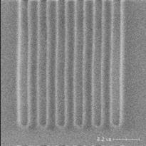
19 J-FIL Template Fabrication Schemes Resist Cr To minimize these effects, reduce the Cr thickness 6025 Quartz Resist applied to <15 nm of Cr Expose/develop e-beam resist, descum Etch chrome, strip resist Etch quartz, Strip chrome Compatible with existing Mask Shop Processes Following Slides: Leica VB6 operating at 100 kv 5 nm address grid ZEP520 positive e-beam resist Track processing on an EVG 150/160 Etching: Unaxis VLR Gas Chemistry: Cr Cl 2 /O 2, SiO 2 CF 4 /O 2
20 ZEP520 Exposure/Descum ZEP520A process latitude is excellent 2.6nm change for every 20 seconds Resist (nm) Resist Descum Cr Etch Quartz Etch Final CD Bias (nm) nm l/s 80 nm l/s 100 nm l/s Exposure Dose ( C/cm 2 ) Descum Time (s)


21 Cr Process CD Results Final CD Bias (nm) s descum s descum 60 s descum Chrome Overetch (%) 60% 80% 100% 120% All results shown are for 80 nm features. Similar to observations made for increasing descum time, a positive CD change of 3.8 nm per 20% of Cr overetch exists.


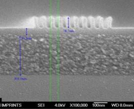
22 FIB/TEM Feature Profile Cross-sectioning the trenches was done using a focused ion beam tool in conjunction with a protective film stack to avoid extreme charging, sample drift, and surface damage. PF PF Using TEM measurements as a basis, sidewall angles of 150 nm features were calculated to be ~ 84 The measured etch depth of 98 nm compares extremely well to profilometer and AFM measurements.
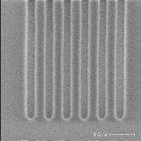
23 Fabrication Window A 20 s descum coupled with a 110% Cr overetch was found to give the best performance in terms of CD control and line edge roughness. CD Bias from Coded (nm) nm features 80 nm features 100 nm features Resist Cr Etch Final Descum Quartz Etch For 60 nm clustered features, the spaces measure ~ 4 nm over coded size. The descum process increases CD by about the same magnitude. Resist erosion during Cr etch results in approximately 7 more nanometers of bias. After quartz etch, CD bias is 1.5 nm less than coded. The quartz sidewall angle is about 5 from the normal Final CD bias ends up approximately 1 nm from coded after the Cr hardmask is stripped.
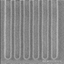
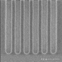
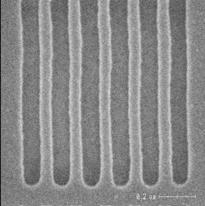
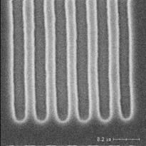
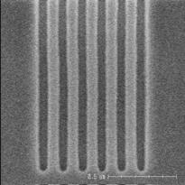
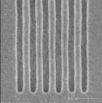
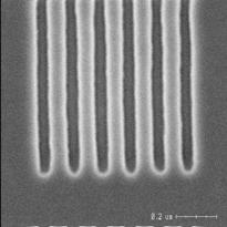
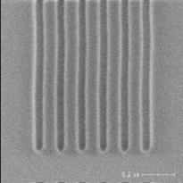
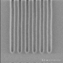
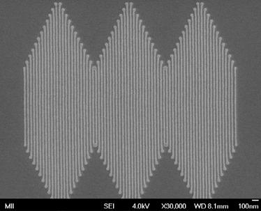
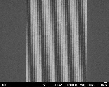
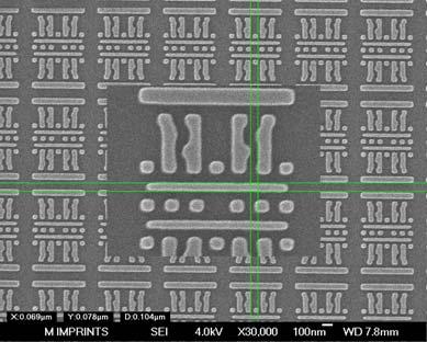
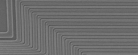
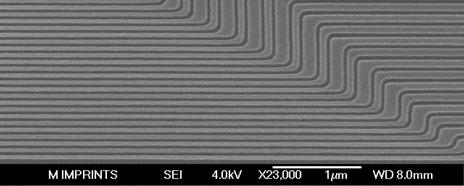
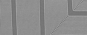
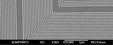
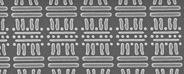
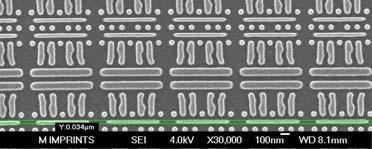
24 Pattern/Pattern Transfer Process Resist Descum Cr Etch Resist Strip Quartz Etch 60 nm 40 nm 30 nm SPIE: Feb 2002


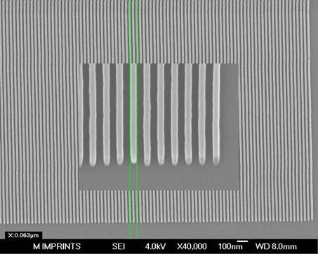
25 Pattern Transfer Process Magnification : 150k PMJ: April 2008
26
27 Electron Beam Pattern Generators There are two methods for generating patterns on a template: 1. Gaussian beam PGs: Great for unit process development and device prototyping 2. Variable Shaped Beam PGs: Needed for full field pattern generation and for image placement How do I get the best result from each tool? Resolution Line Width Roughness CD uniformity Image Placement Write Time
28 Gaussian Beam Pattern Generators
29 ZEP520A Process Development Resist response was studied for a variety of different developers Exposure latitude of the resist was mapped as a function of feature bias Dose ( C/cm2) Relative thickness remaining 1.0E E E Xylenes o-xylene Amyl acetate Hexyl acetate Measured resist CD (nm) Numbers next to curves indicate the digitized CD 40 nm 30 nm 80 nm pitch grating 20 nm CD Dose (uc/cm2) Amyl Acetate developer provides a good combination of contrast and sensitivity Exposure latitude is improves as biasing of critical features increases

 22 20 24 nm 22 nm 18 20 nm 16 18 nm 14 12 200 300 400 500 600 CD normalized dose")
30 Development of ZEP520A resist Sonication of developer bath Dilution of developer Equal mixture of amyl acetate with isopropyl alcohol Negative bias of 12 nm 120 s puddle development s isopropyl alcohol rinse, dry 22 nm half-pitch 18 nm half-pitch CD (nm) nm 22 nm nm nm CD normalized dose ( C/cm2)
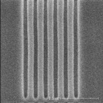
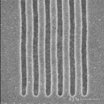
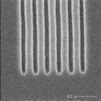
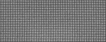
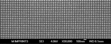
31 Imprint Resolution 28nm half-pitch 25nm Contacts 22nm half-pitch 22nm Fan-out 20nm Half Pitch 20nm Half Pitch
 2007 2010 2013 2016 2019 DRAM Half- Pitch 65 45 32 22 16 LWR 3.4 2.4 1.7 1.2 0.8 Future nodes have no known solutions.")
32 Line Width Roughness (LWR) Variation in CD along the length of a line Results in variation of MOS gate width Affects device speed of individual transistors Leads to IC timing issues ITRS Roadmap for LWR (nm, 3 ) DRAM Half- Pitch LWR Future nodes have no known solutions. 100 nm
 Resolution LWR ~ 6-8 nm (SPIE) So, is imprint lithography immune to this problem? YES!")
33 LWR Example: EUVL Throughput requirements of EUVL require the use of fast chemically amplified resists Low exposure doses required for throughput Too few photons: ~2 / nm 2 Shot noise effects RLS Trade-Off for Chemically Amplified Resists Resolution vs. LWR vs. Sensitivity (Robert Brainard, Gregg Gallatin) Resolution LWR ~ 6-8 nm (SPIE) So, is imprint lithography immune to this problem? YES! And NO!!


34 Pattern formation with J-FIL technology Imprint Mask Fabrication Resolution and LWR Imprint Patterning Throughput Use non-ca resists for best resolution and LWR performance. Utilize existing photomask infrastructure for fabrication and inspection. CD, CDU, LWR, etc. of the patterned resist is determined by the template.
 26 22 18 4 3 2 LWR, 3 (nm)")


35 LWR minimization at 22 nm 34 CD 6 Under Exposed 30 5 LWR=3.29nm Correctly Exposed CD (nm) LWR, 3 (nm) LWR=2.45nm 14 LWR = 2.45 nm, 3 1 Over Exposed Parameter mean LWR=4.27nm Line Width, nm LWR <3 >, nm nm HP nm normalized dose ( C/cm2) 250 C/cm 2 : ~15 electrons / nm 2 Gaussian E-Beam exposure at 100kV 0

36 Template: CD and LWR Analysis 32nm Measured CD (nm) CD LWR, 3 (nm) Parameter Mean, nm Std. dev., nm Line Width LWR <3σ> Left LER <3σ> Right LER <3σ> Pitch Coded CD (nm) CD is linear from 32 to 44nm (to within about 5%) LWR is small, and independent of critical dimension 1 0


37 32nm Imprint Evaluation 32nm #1 LWR=2.55nm #2 LWR=3.05nm Template: LWR = 3.1nm Imprints #1 and #2 are taken from the same location Imprint #3 is located 2mm from Imprint #1 #3 LWR=2.60nm

 = 2.")
38 30 nm and 40 nm design: LWR after etch into SiO 2 30 nm design Field 6 LWR (nm, 3 ) = LER nm design Field 11 LWR (nm, 3 ) = LER 1.01
39 Summary of Line Width Roughness Data LWR (nm, 3sigma) E-beam Template Imprint Etch Fit Measured Feature Size (nm) # lines measured: 170 LWR mean LWR min LWR max 3 = 2.79nm = 1.70nm = 4.39nm = 1.59nm
40 Variable Shape Beam Pattern Generators

41 Variable Shape Beam PGs (VSBs) NuFlare EBM 6000 plus System Architecture VSB systems are e-beam tools of choice for writing 4x photomasks J. Yashima et al, Photomask Japan 2007 Old Wives Tale 9647: VSB tools are the correct choice if you need to write fast, but they don t have great resolution
42 VSB: Commercial Shops CA Resists Logic 80nm 70nm 65 nm grating EIPBN: May 2005


43 Exposure Results: VSBs and ZEP520A ZEP520A Resist Images: EBM nm 45nm 45nm 40nm 50nm 35nm BACUS: September 2007


44 38nm Half Pitch NAND Flash: Gate Level Resolution & LWR both excellent Imprint Results: SPIE: Feb 2008

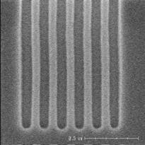
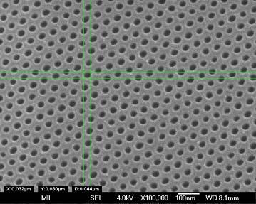
45 VSB: 32nm Imprints 32nm half-pitch 32nm Hor/Vert 32nm x-hatch 32nm HP Pillars 32nm CMOS Test 32nm Metal-1 August 2008


46 Sub-32nm from VSB PGs 22nm Imprint Mask 24nm 28nm 24nm Imprints 26nm 26nm


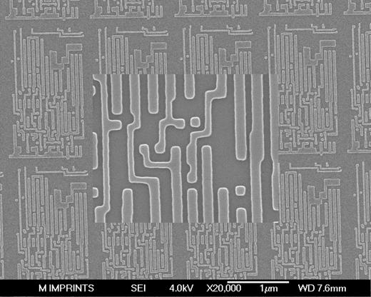
47 Sub 20nm Masks from VSB PGs Current NAND Flash devices are now being fabricated at half pitches of less than 20nm How do we make a sub-20nm mask from a VSB tool? OK, how can they do that?


48 Density Multiplication Density multiplication, also referred to as self aligned spacer double patterning is a standard process of record used to make high density NAND Flash devices SADP SAQP

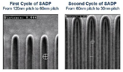
49 Some Density Multiplication Examples SADP SAQP

50 CDU and Image Placement Comparison CD Uniformity Image Placement GB VSB

 Optical mask")

51 Write Time Patterns Reticle A Pattern density: 39.68% Reticle B Pattern density: 15.88% Optical mask A (with OPC) Optical mask B (with OPC) Template A Pattern density: 36.68% Template B Pattern density: 11.78% Template A (without OPC) Template B (without OPC)
52 Write Time Results Pattern A Shot counts [G shot] Writing time [hh:mm:ss] Template, ZEP520A :51:43 4X Mask, FEP :49:18 4X Mask, PRL :24:05 Pattern B Shot counts [G shot] Writing time [hh:mm:ss] Template, ZEP520A :17:29 4X Mask, FEP :48:37 4X Mask, PRL :23:02


53 When all is said and done, e-beam machines are slow! How can we make them write faster? 262,000 beams!!! Probably good for fast mask writing, but maybe never for wafer writing

54 Mask Replication The lifetime of a mask is anticipated to be ~ 50, ,000 imprints An e-beam written master mask will cost ~ $500K If you wanted to print 1M wafers, you would spend ~ $500M on masks Go share that strategy with a fab manager!!! The solution: create a Master Template that can easily be replicated Master Daughter approach Good news! You can use an imprinter to make the Daughter Templates
Development of Nanoimprint Mold Using JBX-9300FS
 Development of Nanoimprint Mold Using JBX-9300FS Morihisa Hoga, Mikio Ishikawa, Naoko Kuwahara Tadahiko Takikawa and Shiho Sasaki Dai Nippon Printing Co., Ltd Research & Development Center Electronic Device
UV Nanoimprint Stepper Technology: Status and Roadmap. S.V. Sreenivasan Sematech Litho Forum May 14 th, 2008
 UV Nanoimprint Stepper Technology: Status and Roadmap S.V. Sreenivasan Sematech Litho Forum May 14 th, 2008 Overview Introduction Stepper technology status: Patterning and CD Control Through Etch Alignment
Major Fabrication Steps in MOS Process Flow
 Major Fabrication Steps in MOS Process Flow UV light Mask oxygen Silicon dioxide photoresist exposed photoresist oxide Silicon substrate Oxidation (Field oxide) Photoresist Coating Mask-Wafer Alignment
Progresses in NIL Template Fabrication Naoya Hayashi
 Progresses in NIL Template Fabrication Naoya Hayashi Electronic Device Operations Dai Nippon Printing Co., Ltd. Contents 1. Introduction Motivation NIL mask fabrication process 2. NIL mask resolution improvement
EUV Interference Lithography in NewSUBARU
 EUV Interference Lithography in NewSUBARU Takeo Watanabe 1, Tae Geun Kim 2, Yasuyuki Fukushima 1, Noki Sakagami 1, Teruhiko Kimura 1, Yoshito Kamaji 1, Takafumi Iguchi 1, Yuuya Yamaguchi 1, Masaki Tada
Section 2: Lithography. Jaeger Chapter 2. EE143 Ali Javey Slide 5-1
 Section 2: Lithography Jaeger Chapter 2 EE143 Ali Javey Slide 5-1 The lithographic process EE143 Ali Javey Slide 5-2 Photolithographic Process (a) (b) (c) (d) (e) (f) (g) Substrate covered with silicon
Design Rules for Silicon Photonics Prototyping
 Design Rules for licon Photonics Prototyping Version 1 (released February 2008) Introduction IME s Photonics Prototyping Service offers 248nm lithography based fabrication technology for passive licon-on-insulator
State-of-the-art device fabrication techniques
 State-of-the-art device fabrication techniques! Standard Photo-lithography and e-beam lithography! Advanced lithography techniques used in semiconductor industry Deposition: Thermal evaporation, e-gun
Section 2: Lithography. Jaeger Chapter 2 Litho Reader. EE143 Ali Javey Slide 5-1
 Section 2: Lithography Jaeger Chapter 2 Litho Reader EE143 Ali Javey Slide 5-1 The lithographic process EE143 Ali Javey Slide 5-2 Photolithographic Process (a) (b) (c) (d) (e) (f) (g) Substrate covered
Electron Multi-Beam Technology for Mask and Wafer Direct Write. Elmar Platzgummer IMS Nanofabrication AG
 Electron Multi-Beam Technology for Mask and Wafer Direct Write Elmar Platzgummer IMS Nanofabrication AG Contents 2 Motivation for Multi-Beam Mask Writer (MBMW) MBMW Tool Principles and Architecture MBMW
Section 2: Lithography. Jaeger Chapter 2 Litho Reader. The lithographic process
 Section 2: Lithography Jaeger Chapter 2 Litho Reader The lithographic process Photolithographic Process (a) (b) (c) (d) (e) (f) (g) Substrate covered with silicon dioxide barrier layer Positive photoresist
EE 143 Microfabrication Technology Fall 2014
 EE 143 Microfabrication Technology Fall 2014 Prof. Clark T.-C. Nguyen Dept. of Electrical Engineering & Computer Sciences University of California at Berkeley Berkeley, CA 94720 EE 143: Microfabrication
TECHNOLOGY ROADMAP 2006 UPDATE LITHOGRAPHY FOR
 INTERNATIONAL TECHNOLOGY ROADMAP FOR SEMICONDUCTORS 2006 UPDATE LITHOGRAPHY THE ITRS IS DEVISED AND INTENDED FOR TECHNOLOGY ASSESSMENT ONLY AND IS WITHOUT REGARD TO ANY COMMERCIAL CONSIDERATIONS PERTAINING
Institute of Solid State Physics. Technische Universität Graz. Lithography. Peter Hadley
 Technische Universität Graz Institute of Solid State Physics Lithography Peter Hadley http://www.cleanroom.byu.edu/virtual_cleanroom.parts/lithography.html http://www.cleanroom.byu.edu/su8.phtml Spin coater
2009 International Workshop on EUV Lithography
 Contents Introduction Absorber Stack Optimization Non-flatness Correction Blank Defect and Its Mitigation Wafer Printing Inspection Actinic Metrology Cleaning and Repair Status Remaining Issues in EUV
Lithography. Development of High-Quality Attenuated Phase-Shift Masks
 Lithography S P E C I A L Development of High-Quality Attenuated Phase-Shift Masks by Toshihiro Ii and Masao Otaki, Toppan Printing Co., Ltd. Along with the year-by-year acceleration of semiconductor device
Part 5-1: Lithography
 Part 5-1: Lithography Yao-Joe Yang 1 Pattern Transfer (Patterning) Types of lithography systems: Optical X-ray electron beam writer (non-traditional, no masks) Two-dimensional pattern transfer: limited
EE143 Fall 2016 Microfabrication Technologies. Lecture 3: Lithography Reading: Jaeger, Chap. 2
 EE143 Fall 2016 Microfabrication Technologies Lecture 3: Lithography Reading: Jaeger, Chap. 2 Prof. Ming C. Wu wu@eecs.berkeley.edu 511 Sutardja Dai Hall (SDH) 1-1 The lithographic process 1-2 1 Photolithographic
Challenges of EUV masks and preliminary evaluation
 Challenges of EUV masks and preliminary evaluation Naoya Hayashi Electronic Device Laboratory Dai Nippon Printing Co.,Ltd. EUV Mask Workshop 2004 1 Contents Recent Lithography Options on Roadmap Challenges
Inspection of templates for imprint lithography
 Inspection of templates for imprint lithography Harald F. Hess, a) Don Pettibone, David Adler, and Kirk Bertsche KLA-Tencor 160 Rio Robles, San Jose, California 95134 Kevin J. Nordquist, David P. Mancini,
Critical Dimension and Image Placement Issues for Step and Flash Imprint Lithography Templates
 Critical Dimension and Image Placement Issues for Step and Flash Imprint Lithography Templates Kevin J. Nordquist 1, David P. Mancini 1, William J. Dauksher 1, Eric S. Ainley 1, Kathy A. Gehoski 1, Douglas
From Possible to Practical The Evolution of Nanoimprint for Patterned Media
 From Possible to Practical The Evolution of Nanoimprint for Patterned Media Paul Hofemann March 13, 2009 HDD Areal Density Industry Roadmap 10,000 Media Technology Roadmap Today Areal Density (Gbit/in
Advanced Patterning Techniques for 22nm HP and beyond
 Advanced Patterning Techniques for 22nm HP and beyond An Overview IEEE LEOS (Bay Area) Yashesh A. Shroff Intel Corporation Aug 4 th, 2009 Outline The Challenge Advanced (optical) lithography overview Flavors
Generating integrated-circuit patterns via cutting and stitching of gratings
 Purdue University Purdue e-pubs Birck and NCN Publications Birck Nanotechnology Center 11-2009 Generating integrated-circuit patterns via cutting and stitching of gratings Lin Zhao Purdue University -
5. Lithography. 1. photolithography intro: overall, clean room 2. principle 3. tools 4. pattern transfer 5. resolution 6. next-gen
 5. Lithography 1. photolithography intro: overall, clean room 2. principle 3. tools 4. pattern transfer 5. resolution 6. next-gen References: Semiconductor Devices: Physics and Technology. 2 nd Ed. SM
Photolithography I ( Part 1 )
") 1 Photolithography I ( Part 1 ) Chapter 13 : Semiconductor Manufacturing Technology by M. Quirk & J. Serda Bjørn-Ove Fimland, Department of Electronics and Telecommunication, Norwegian University of Science
1 Photolithography I ( Part 1 ) Chapter 13 : Semiconductor Manufacturing Technology by M. Quirk & J. Serda Bjørn-Ove Fimland, Department of Electronics and Telecommunication, Norwegian University of Science
Development of a LFLE Double Pattern Process for TE Mode Photonic Devices. Mycahya Eggleston Advisor: Dr. Stephen Preble
 Development of a LFLE Double Pattern Process for TE Mode Photonic Devices Mycahya Eggleston Advisor: Dr. Stephen Preble 2 Introduction and Motivation Silicon Photonics Geometry, TE vs TM, Double Pattern
Holistic View of Lithography for Double Patterning. Skip Miller ASML
 Holistic View of Lithography for Double Patterning Skip Miller ASML Outline Lithography Requirements ASML Holistic Lithography Solutions Conclusions Slide 2 Shrink Continues Lithography keeps adding value
Nanofluidic Diodes based on Nanotube Heterojunctions
 Supporting Information Nanofluidic Diodes based on Nanotube Heterojunctions Ruoxue Yan, Wenjie Liang, Rong Fan, Peidong Yang 1 Department of Chemistry, University of California, Berkeley, CA 94720, USA
Imec pushes the limits of EUV lithography single exposure for future logic and memory
 Edition March 2018 Semiconductor technology & processing Imec pushes the limits of EUV lithography single exposure for future logic and memory Imec has made considerable progress towards enabling extreme
Cost of Ownership Analysis for Patterning Using Step and Flash Imprint Lithography
 Cost of Ownership Analysis for Patterning Using Step and Flash Imprint Lithography S.V. Sreenivasan 1, C.G. Willson 2, N.E. Schumaker 3, D.J. Resnick 4 1 Mechanical Engineering, University of Texas at
Clean Room Technology Optical Lithography. Lithography I. takenfrombdhuey
 Clean Room Technology Optical Lithography Lithography I If the automobile had followed the same development cycle as the computer, a Rolls Royce would today cost $100, get a million miles per gallon, and
Semiconductor Manufacturing Technology. Semiconductor Manufacturing Technology. Photolithography: Resist Development and Advanced Lithography
 Semiconductor Manufacturing Technology Michael Quirk & Julian Serda October 2001 by Prentice Hall Chapter 15 Photolithography: Resist Development and Advanced Lithography Eight Basic Steps of Photolithography
Strategies for low cost imprint molds
 Strategies for low cost imprint molds M.P.C. Watts, Impattern Solutions, 9404 Bell Mountain Drive Austin TX 78730 www.impattern.com ABSTRACT The Cost of ownership (COO) due to the mold can be minimized
Module 11: Photolithography. Lecture 14: Photolithography 4 (Continued)
") Module 11: Photolithography Lecture 14: Photolithography 4 (Continued) 1 In the previous lecture, we have discussed the utility of the three printing modes, and their relative advantages and disadvantages.
Module 11: Photolithography Lecture 14: Photolithography 4 (Continued) 1 In the previous lecture, we have discussed the utility of the three printing modes, and their relative advantages and disadvantages.
Process Optimization
 Process Optimization Process Flow for non-critical layer optimization START Find the swing curve for the desired resist thickness. Determine the resist thickness (spin speed) from the swing curve and find
TECHNOLOGY ROADMAP 2011 EDITION LITHOGRAPHY FOR
 INTERNATIONAL TECHNOLOGY ROADMAP FOR SEMICONDUCTORS 2011 EDITION LITHOGRAPHY THE ITRS IS DEVISED AND INTENDED FOR TECHNOLOGY ASSESSMENT ONLY AND IS WITHOUT REGARD TO ANY COMMERCIAL CONSIDERATIONS PERTAINING
Copyright 2000, Society of Photo-Optical Instrumentation Engineers This paper was published in Optical Microlithography XIII, Volume 4000 and is made
 Copyright 00, Society of Photo-Optical Instrumentation Engineers This paper was published in Optical Microlithography XIII, Volume 4000 and is made available as an electronic reprint with permission of
Copyright 1998 by the Society of Photo-Optical Instrumentation Engineers.
 Copyright 998 by the Society of Photo-Optical Instrumentation Engineers. This paper was published in the proceedings of the 8 th Annual BACUS Symposium on Photomask Technology and Management SPIE Vol.
Multi-beam mask writer MBM-1000 for advanced mask making
 Multi-beam mask writer MBM-1000 for advanced mask making H. Matsumoto NuFlare Technology, Inc. Slide 1 Multi-beam Shaping aperture array (SAA) Blanking aperture array (BAA) Sub deflectors Main deflectors
The Development of Full Field High Resolution Imprint Templates
 The Development of Full Field High Resolution Imprint Templates Shusuke Yoshitake 1, Hitoshi Sunaoshi 1, Kenichi Yasui 1, Hideo Kobayashi 2, Takashi Sato 2, Osamu Nagarekawa 2, Ecron Thompson 3, Gerard
Lecture 7. Lithography and Pattern Transfer. Reading: Chapter 7
 Lecture 7 Lithography and Pattern Transfer Reading: Chapter 7 Used for Pattern transfer into oxides, metals, semiconductors. 3 types of Photoresists (PR): Lithography and Photoresists 1.) Positive: PR
Lithography Roadmap. without immersion lithography. Node Half pitch. 248nm. 193nm. 157nm EUVL. 3-year cycle: 2-year cycle: imec 2005
 Lithography Roadmap without immersion lithography Node Half pitch 180 nm 130 nm 90 nm 65 nm 45 nm 32 nm 22 nm 250 nm 180 nm 130 nm 90 nm 65 nm 45 nm 32 nm 248nm 193nm 157nm EUVL 3-year cycle: 2-year cycle:
Lecture 13 Basic Photolithography
 Lecture 13 Basic Photolithography Chapter 12 Wolf and Tauber 1/64 Announcements Homework: Homework 3 is due today, please hand them in at the front. Will be returned one week from Thursday (16 th Nov).
INTERNATIONAL TECHNOLOGY ROADMAP LITHOGRAPHY FOR SEMICONDUCTORS 2009 EDITION
 INTERNATIONAL TECHNOLOGY ROADMAP FOR SEMICONDUCTORS 2009 EDITION LITHOGRAPHY THE ITRS IS DEVISED AND INTENDED FOR TECHNOLOGY ASSESSMENT ONLY AND IS WITHOUT REGARD TO ANY COMMERCIAL CONSIDERATIONS PERTAINING
Results of Proof-of-Concept 50keV electron multi-beam Mask Exposure Tool (emet POC)
") Results of Proof-of-Concept 50keV electron multi-beam Mask Exposure Tool (emet POC) Elmar Platzgummer *, Christof Klein, and Hans Loeschner IMS Nanofabrication AG Schreygasse 3, A-1020 Vienna, Austria
Results of Proof-of-Concept 50keV electron multi-beam Mask Exposure Tool (emet POC) Elmar Platzgummer *, Christof Klein, and Hans Loeschner IMS Nanofabrication AG Schreygasse 3, A-1020 Vienna, Austria
MAPPER: High throughput Maskless Lithography
 MAPPER: High throughput Maskless Lithography Marco Wieland CEA- Leti Alterative Lithography workshop 1 Today s agenda Introduction Applications Qualification of on-tool metrology by in-resist metrology
Dr. Dirk Meyners Prof. Wagner. Wagner / Meyners Micro / Nanosystems Technology
 Micro/Nanosystems Technology Dr. Dirk Meyners Prof. Wagner 1 Outline - Lithography Overview - UV-Lithography - Resolution Enhancement Techniques - Electron Beam Lithography - Patterning with Focused Ion
* AIT-5: Maskless, High-NA, Immersion, EUV, Imprint
 Advanced Issues and Technology (AIT) Modules Purpose: Explain the top advanced issues and concepts in optical projection printing and electron-beam lithography. AIT-1: LER and CAR AIT-2: Resolution Enhancement
Feature-level Compensation & Control
 Feature-level Compensation & Control 2 Sensors and Control Nathan Cheung, Kameshwar Poolla, Costas Spanos Workshop 11/19/2003 3 Metrology, Control, and Integration Nathan Cheung, UCB SOI Wafers Multi wavelength
Low-Cost Nanostructure Patterning Using Step and Flash Imprint Lithography
 Low-Cost Nanostructure Patterning Using Step and Flash Imprint Lithography S.V. Sreenivasan 1, C.G. Willson 2, N.E. Schumaker 3, D.J. Resnick 4 1 Mechanical Engineering, University of Texas at Austin 2
Micro-Nanofabrication
 Zheng Cui Micro-Nanofabrication TECHNOLOGIES AND APPLICATIONS ^f**"?* ö Springer Higher Education Press -T O Table of Content Preface About the Author Chapter 1 Introduction 1 1.1 Micro-nanotechnologies
Introduction of ADVANTEST EB Lithography System
 Introduction of ADVANTEST EB Lithography System Nanotechnology Business Division ADVANTEST Corporation 1 2 Node [nm] EB Lithography Products < ADVANTEST s Superiority > High Resolution :EB optical technology
Quantized patterning using nanoimprinted blanks
 IOP PUBLISHING Nanotechnology 20 (2009) 155303 (7pp) Quantized patterning using nanoimprinted blanks NANOTECHNOLOGY doi:10.1088/0957-4484/20/15/155303 Stephen Y Chou 1, Wen-Di Li and Xiaogan Liang NanoStructure
High throughput ultra-long (20cm) nanowire fabrication using a. wafer-scale nanograting template
 nanowire fabrication using a. wafer-scale nanograting template") Supporting Information High throughput ultra-long (20cm) nanowire fabrication using a wafer-scale nanograting template Jeongho Yeon 1, Young Jae Lee 2, Dong Eun Yoo 3, Kyoung Jong Yoo 2, Jin Su Kim 2,
Supporting Information High throughput ultra-long (20cm) nanowire fabrication using a wafer-scale nanograting template Jeongho Yeon 1, Young Jae Lee 2, Dong Eun Yoo 3, Kyoung Jong Yoo 2, Jin Su Kim 2,
Lithography. 3 rd. lecture: introduction. Prof. Yosi Shacham-Diamand. Fall 2004
 Lithography 3 rd lecture: introduction Prof. Yosi Shacham-Diamand Fall 2004 1 List of content Fundamental principles Characteristics parameters Exposure systems 2 Fundamental principles Aerial Image Exposure
ECSE 6300 IC Fabrication Laboratory Lecture 3 Photolithography. Lecture Outline
 ECSE 6300 IC Fabrication Laboratory Lecture 3 Photolithography Prof. James J. Q. Lu Bldg. CII, Rooms 6229 Rensselaer Polytechnic Institute Troy, NY 12180 Tel. (518)276 2909 e mails: luj@rpi.edu http://www.ecse.rpi.edu/courses/s18/ecse
DTU DANCHIP an open access micro/nanofabrication facility bridging academic research and small scale production
 DTU DANCHIP an open access micro/nanofabrication facility bridging academic research and small scale production DTU Danchip National Center for Micro- and Nanofabrication DTU Danchip DTU Danchip is Denmark
Optolith 2D Lithography Simulator
 2D Lithography Simulator Advanced 2D Optical Lithography Simulator 4/13/05 Introduction is a powerful non-planar 2D lithography simulator that models all aspects of modern deep sub-micron lithography It
Machine-Aligned Fabrication of Submicron SIS Tunnel Junctions Using a Focused Ion Beam
 Machine-Aligned Fabrication of Submicron SIS Tunnel Junctions Using a Focused Ion Beam Robert. B. Bass, Jian. Z. Zhang and Aurthur. W. Lichtenberger Department of Electrical Engineering, University of
Evaluation of the Imprio 100 Step and Flash Imprint Lithography Tool
 Evaluation of the Imprio 100 Step and Flash Imprint Lithography Tool Kathleen A. Gehoski, David P. Mancini, Douglas J. Resnick Microelectronics and Physical Sciences Laboratories, Motorola Labs, Tempe,
Monolithically integrated InGaAs nanowires on 3D. structured silicon-on-insulator as a new platform for. full optical links
 Monolithically integrated InGaAs nanowires on 3D structured silicon-on-insulator as a new platform for full optical links Hyunseok Kim 1, Alan C. Farrell 1, Pradeep Senanayake 1, Wook-Jae Lee 1,* & Diana.
CRITICAL DIMENSION CONTROL, OVERLAY, AND THROUGHPUT BUDGETS IN UV NANOIMPRINT STEPPER TECHNOLOGY
 CRITICAL DIMENSION CONTROL, OVERLAY, AND THROUGHPUT BUDGETS IN UV NANOIMPRINT STEPPER TECHNOLOGY S.V. Sreenivasan 1, 2, P.D. Schumaker 2, B.J. Choi 2 1 Department of Mechanical Engineering University of
EG2605 Undergraduate Research Opportunities Program. Large Scale Nano Fabrication via Proton Lithography Using Metallic Stencils
 EG2605 Undergraduate Research Opportunities Program Large Scale Nano Fabrication via Proton Lithography Using Metallic Stencils Tan Chuan Fu 1, Jeroen Anton van Kan 2, Pattabiraman Santhana Raman 2, Yao
Image placement issues for ITO-based step and flash imprint lithography templates
 Image placement issues for ITO-based step and flash imprint lithography templates K. J. Nordquist, a) E. S. Ainley, D. P. Mancini, W. J. Dauksher, K. A. Gehoski, J. Baker, and D. J. Resnick Motorola Labs,
INTERNATIONAL TECHNOLOGY ROADMAP SEMICONDUCTORS 2001 EDITION LITHOGRAPHY FOR
 INTERNATIONAL TECHNOLOGY ROADMAP FOR SEMICONDUCTORS 2001 EDITION LITHOGRAPHY TABLE OF CONTENTS Scope...1 Difficult Challenges...1 Lithography Technology Requirements...3 Potential Solutions...14 Crosscut
Toward 5nm node ; Untoward Scaling with Multi-patterning
 1 st International Symposium on DSA Toward 5nm node ; Untoward Scaling with Multi-patterning 27 th OCT 2015 H. Yaegashi Chief Engineer Tokyo Electron Limited Down-caling trend towards N5 N20 N14 N10 N7
Micro- and Nano- Fabrication and Replication Techniques
 Micro- and Nano- Fabrication and Replication Techniques Why do we have to write thing small and replicate fast? Plenty of Room at the Bottom Richard P. Feynman, December 1959 How do we write it? We have
What s So Hard About Lithography?
 What s So Hard About Lithography? Chris A. Mack, www.lithoguru.com, Austin, Texas Optical lithography has been the mainstay of semiconductor patterning since the early days of integrated circuit production.
Optical Bus for Intra and Inter-chip Optical Interconnects
 Optical Bus for Intra and Inter-chip Optical Interconnects Xiaolong Wang Omega Optics Inc., Austin, TX Ray T. Chen University of Texas at Austin, Austin, TX Outline Perspective of Optical Backplane Bus
Optical Lithography. Keeho Kim Nano Team / R&D DongbuAnam Semi
 Optical Lithography Keeho Kim Nano Team / R&D DongbuAnam Semi Contents Lithography = Photolithography = Optical Lithography CD : Critical Dimension Resist Pattern after Development Exposure Contents Optical
Copyright 2000 by the Society of Photo-Optical Instrumentation Engineers.
 Copyright 2000 by the Society of Photo-Optical Instrumentation Engineers. This paper was published in the proceedings of the 20 th Annual BACUS Symposium on Photomask Technology SPIE Vol. 4186, pp. 503-507.
immersion optics Immersion Lithography with ASML HydroLith TWINSCAN System Modifications for Immersion Lithography by Bob Streefkerk
 immersion optics Immersion Lithography with ASML HydroLith by Bob Streefkerk For more than 25 years, many in the semiconductor industry have predicted the end of optical lithography. Recent developments,
Lecture 8. Microlithography
 Lecture 8 Microlithography Lithography Introduction Process Flow Wafer Exposure Systems Masks Resists State of the Art Lithography Next Generation Lithography (NGL) Recommended videos: http://www.youtube.com/user/asmlcompany#p/search/1/jh6urfqt_d4
Defect inspection of imprinted 32 nm half pitch patterns
 Defect inspection of imprinted 32 nm half pitch patterns Kosta Selinidis, Ecron Thompson, Ian McMackin, Joseph Perez, S.V. Sreenivasan, Douglas J. Resnick Molecular Imprints, Inc., 1807 West Braker Lane,
Multiple Patterning for Immersion Extension and EUV Insertion. Chris Bencher Distinguished Member of Technical Staff Applied Materials CTO group
 Multiple Patterning for Immersion Extension and EUV Insertion Chris Bencher Distinguished Member of Technical Staff Applied Materials CTO group Abstract Multiple Patterning for Immersion Extension and
Nanoscale Lithography. NA & Immersion. Trends in λ, NA, k 1. Pushing The Limits of Photolithography Introduction to Nanotechnology
 15-398 Introduction to Nanotechnology Nanoscale Lithography Seth Copen Goldstein Seth@cs.cmu.Edu CMU Pushing The Limits of Photolithography Reduce wavelength (λ) Use Reducing Lens Increase Numerical Aperture
FABRICATION OF CMOS INTEGRATED CIRCUITS. Dr. Mohammed M. Farag
 FABRICATION OF CMOS INTEGRATED CIRCUITS Dr. Mohammed M. Farag Outline Overview of CMOS Fabrication Processes The CMOS Fabrication Process Flow Design Rules Reference: Uyemura, John P. "Introduction to
Optical Lithography. Here Is Why. Burn J. Lin SPIE PRESS. Bellingham, Washington USA
 Optical Lithography Here Is Why Burn J. Lin SPIE PRESS Bellingham, Washington USA Contents Preface xiii Chapter 1 Introducing Optical Lithography /1 1.1 The Role of Lithography in Integrated Circuit Fabrication
Photolithography Technology and Application
 Photolithography Technology and Application Jeff Tsai Director, Graduate Institute of Electro-Optical Engineering Tatung University Art or Science? Lind width = 100 to 5 micron meter!! Resolution = ~ 3
Real time plasma etch control by means of physical plasma parameters with HERCULES
 Real time plasma etch control by means of physical plasma parameters with HERCULES A. Steinbach 1) S. Bernhard 1) M. Sussiek 4) S. Wurm 2) Ch. Koelbl 3) D. Knobloch 1) Siemens, Dresden Siemens at International
Contrast Enhancement Materials CEM 365HR
 INTRODUCTION In 1989 Shin-Etsu Chemical acquired MicroSi, Inc. including their Contrast Enhancement Material (CEM) technology business*. A concentrated effort in the technology advancement of a CEM led
University of California, Berkeley Department of Mechanical Engineering. ME 290R Topics in Manufacturing, Fall 2014: Lithography
 University of California, Berkeley Department of Mechanical Engineering ME 290R Topics in Manufacturing, Fall 2014: Lithography Class meetings: TuTh 3.30 5pm in 1165 Etcheverry Tentative class schedule
Multi-Beam activity from the 1980s. Apr 18, 2013 Panel Discussion Photomask Japan 2013
 Multi-Beam activity from the 1980s 1 Panel Discussion Multi-Beam Mask Writer Hans Loeschner IMS Nanofabrication AG Vienna, Austria Jiun Sonja (1718-1805) Buji Kore Kinin Only those who live simply, live
Device Fabrication: Photolithography
 Device Fabrication: Photolithography 1 Objectives List the four components of the photoresist Describe the difference between +PR and PR Describe a photolithography process sequence List four alignment
Status and Challenges for Multibeam DW lithography. L. PAIN CEA - LETI Silicon Technology Department
 Status and Challenges for Multibeam DW lithography L. PAIN CEA - LETI Silicon Technology Department Outline Introduction Challenges Current program status KLA-TENCOR MAPPER Demonstration capability IMAGINE
EUVL getting ready for volume introduction
 EUVL getting ready for volume introduction SEMICON West 2010 Hans Meiling, July 14, 2010 Slide 1 public Outline ASML s Lithography roadmap to support Moore s Law Progress on 0.25NA EUV systems Progress
Sub-12nm Optical Lithography with 4x Pitch Division and SMO-Lite
 Sub-12nm Optical Lithography with 4x Pitch Division and SMO-Lite Michael C. Smayling* a, Koichiro Tsujita b, Hidetami Yaegashi c, Valery Axelrad d Tadashi Arai b, Kenichi Oyama c, Arisa Hara c a Tela Innovations,
AOARD REPORT The Photomask Japan '94 Held 22 April 94 at Kawasaki Science Park, Kanagawa, Japan
 > AOARD-TR-94-22 AOARD REPORT The Photomask Japan '94 Held 22 April 94 at Kawasaki Science Park, Kanagawa, Japan 22 April 1994 S. J. Yakura AOARD The Photomask Japan '94 symposium, the first photomask
Mask Technology Development in Extreme-Ultraviolet Lithography
 Mask Technology Development in Extreme-Ultraviolet Lithography Anthony Yen September 6, 2013 Projected End of Optical Lithography 2013 TSMC, Ltd 1976 1979 1982 1985 1988 1991 1994 1997 2000 2003 2007 2012
Fabrication Techniques of Optical ICs
 Fabrication Techniques of Optical ICs Processing Techniques Lift off Process Etching Process Patterning Techniques Photo Lithography Electron Beam Lithography Photo Resist ( Microposit MP1300) Electron
DOE Project: Resist Characterization
 DOE Project: Resist Characterization GOAL To achieve high resolution and adequate throughput, a photoresist must possess relatively high contrast and sensitivity to exposing radiation. The objective of
COMPARISON OF ULTIMATE RESOLUTION ACHIEVED BY E-BEAM WRITERS WITH SHAPED BEAM AND WITH GAUSSIAN BEAM
 COMPARISON OF ULTIMATE RESOLUTION ACHIEVED BY E-BEAM WRITERS WITH SHAPED BEAM AND WITH GAUSSIAN BEAM Stanislav KRÁTKÝ a, Vladimír KOLAŘÍK a, Milan MATĚJKA a, Michal URBÁNEK a, Miroslav HORÁČEK a, Jana
Shot noise and process window study for printing small contacts using EUVL. Sang Hun Lee John Bjorkohlm Robert Bristol
 Shot noise and process window study for printing small contacts using EUVL Sang Hun Lee John Bjorkohlm Robert Bristol Abstract There are two issues in printing small contacts with EUV lithography (EUVL).
A process for, and optical performance of, a low cost Wire Grid Polarizer
 1.0 Introduction A process for, and optical performance of, a low cost Wire Grid Polarizer M.P.C.Watts, M. Little, E. Egan, A. Hochbaum, Chad Jones, S. Stephansen Agoura Technology Low angle shadowed deposition
Sub-50 nm period patterns with EUV interference lithography
 Microelectronic Engineering 67 68 (2003) 56 62 www.elsevier.com/ locate/ mee Sub-50 nm period patterns with EUV interference lithography * a, a a b b b H.H. Solak, C. David, J. Gobrecht, V. Golovkina,
Micro- and Nano-Technology... for Optics
 Micro- and Nano-Technology...... for Optics 3.2 Lithography U.D. Zeitner Fraunhofer Institut für Angewandte Optik und Feinmechanik Jena Printing on Stones Map of Munich Stone Print Shadow Printing Photomask
Lithographic Performance and Mix-and-Match Lithography using 100 kv Electron Beam System JBX-9300FS
 Lithographic Performance and Mix-and-Match Lithography using 100 kv Electron Beam System JBX-9300FS Yukinori Ochiai, Takashi Ogura, Mitsuru Narihiro, and Kohichi Arai Silicon Systems Research Laboratories,
Low-power carbon nanotube-based integrated circuits that can be transferred to biological surfaces
 SUPPLEMENTARY INFORMATION Articles https://doi.org/10.1038/s41928-018-0056-6 In the format provided by the authors and unedited. Low-power carbon nanotube-based integrated circuits that can be transferred
Exhibit 2 Declaration of Dr. Chris Mack
 STC.UNM v. Intel Corporation Doc. 113 Att. 5 Exhibit 2 Declaration of Dr. Chris Mack Dockets.Justia.com UNITED STATES DISTRICT COURT DISTRICT OF NEW MEXICO STC.UNM, Plaintiff, v. INTEL CORPORATION Civil