Sensors and Metrology - 2 Optical Microscopy and Overlay Measurements
|
|
|
- Arthur Morgan
- 6 years ago
- Views:
Transcription
1 Sensors and Metrology - 2 Optical Microscopy and Overlay Measurements 1
2 Optical Metrology Optical Microscopy What is its place in IC production? What are the limitations and the hopes? The issue of Alignment Control Needs in the industry Basic technology Precision and Accuracy of existing tools How the future looks 2
3 Optical Microscopy Optical Microscopes have limited resolution, but are still useful instruments for human (or even automated) inspection: R = 0.61λ/NA NA = n sinα Overview of Optical Microscopy and Optical Microspectroscopy, Joel W. Ager III, Characterization and Metrology for ULSI Technology, 1998 International Conference. 3

4 General Configuration Practical magnification levels are limited by the diffractionlimited resolution... 4
5 Typical Resolution Limits Resolution defined as the minimum distance at which two bright spots can be distinguished. 5
6 Confocal Microscopy for Enhanced Resolution Focused laser beam is scanned across field of view, image is reconstructed electronically. 6
7 Ultraviolet Microscopy with NA>1 (!) UV illumination NA > 1 (achieved by immersing lens in high n medium (glycerin) Very high resolution, and very, very thin depth of focus. Can be useful in detecting buried defects! Contamination concerns limit use in IC production 7
.")
8 Near-field Scanning Optical Microscopy Use very narrow fiber (50-100nm) to illuminate at near field, and detect at far field, or a focused laser to illuminate at far field and narrow fiber to detect at near field. Either case requires AFM-like scanning and feedback control for position (terrain following). Approach limited by speed and surface topography. 8

9 Microscopy can help in Contamination Analysis 9
10 Raman Microspectroscopy Microspectroscopy is considered a very promising technique for defect classification 10
11 Raman Spectroscopy for Defect Classification 11


12 The Issue of Image Placement 12
 Random (pattern dependent, CMP effects, etc.")
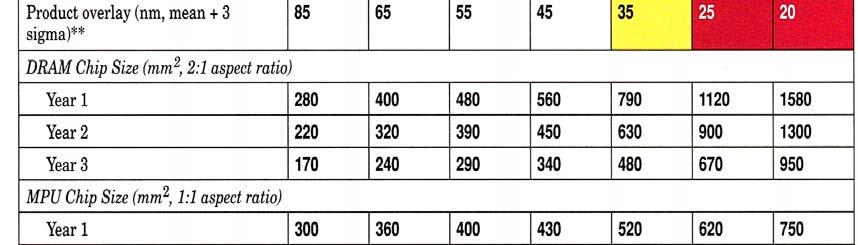
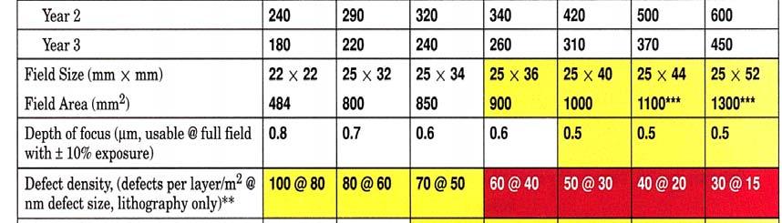
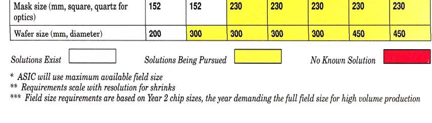
13 Overlay Requirements 0.5μm technology needed 150nm of overlay 0.25μm technology needs <100nm of overlay 3-5% of overlay budget can be allowed for metrology errors. Systematic (lens aberrations, illumination problems, wafer related problems, resist slope, processing asymmetry, etc.) Random (pattern dependent, CMP effects, etc.) Ugly (interactions among process steps, strange sensitivity to focus position, etc.) 13
14 Image Placement Metrology of Image Placement, Alexander Starikov, Ultratech Stepper, Inc., San Jose, California CP449, Characterization and Metrology for ULSI Technology: 1998 International Conference, edited by D. G. Seiler, A. C. Diebold, W. M. Bullis, T. J. Shaffner, R. McDonald, and E. J. Walters 14
15 Typical redundant target Overlay Metrology: The systematic, the random and the ugly, Neal Sullivan, Jennifer Shin, Advanced Process Tool Development Group, Digital Semiconductor, Hudson, MA CP449, Characterization and Metrology for ULSI Technology: 1998 International Conference edited by D. G. Seiler, A. C. Diebold, W. M. Bullis, T. J. Shaffner, R. McDonald, and E. J. Walters The American Institute of Physics l /98/$
16 Standard SEMI Targets Modern targets exploit dimensional redundancy TIS (Tool Induced Shift) can be measured by comparing readings to 180 degree rotation. WIS (Wafer induced Shift) is subject to topography and other target problems. It is much harder to measure. 16

17 Target Asymmetry can be a Problem 17
18 An Illustration of TIS and WIS effects 18
19 Tool-to-Tool matching is an issue 19
20 Imaged-based Error Correction helps... 20
21 Other issues contribute to variability 21

22 W CMP Case Study CMP is meant to planarize We need visible edges to measure centerlines and adjust position. Some undesirable CMP artifacts help us find position. 22


23 Optical and Electronic Tricks help Placement error is proportional to square root of noise... 23

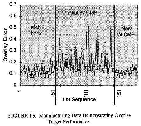
24 Results of W CMP study 24
25 W-CMP Study 1) Substrate bar formed by isolated space to avoid erosion. 2) Maximize edge definition by maximizing post W CMP Step height: a) Minimized deposited W thickness b) Optimize trench width to 6-8 times minimum feature size (Max width determined by dishing). c) maximize trench depth (remove etch stops). Note conflicting process/metrology requirements! 25


26 Modern Tools are big, dedicated and expensive 26
27 Approach for Metrology Improvement use a comprehensive (system-wide) approach; analyze processes, sub-processes and points of hand-off; establish quantitative measures of metrology quality; automate gathering and analyses of quality feedback; assess quality of typical metrology (benchmarking); assess the failures of control (frequency and magnitude); establish the absolute values of error (to standard); account for technology limitations; rank the impact and cost to remove (Pareto analysis); remove the largest detractors first and re-assess. 27
28 Metrology The ultimate goal of IC manufacturing is to make high quality product at reasonable cost, so that the people in metrology and processing make their living. When the social contract of the various groups involved in IC manufacture is seen this way, a solution is always found. 28
29 What is next In-situ possibilities Reflectometry, Ellipsometry and Scatterometry OES, Temperature, Pressure Sensors What is the future in process/wafer sensors? 29
Managing Within Budget
 Overlay M E T R O L OProcess G Y Control Managing Within Budget Overlay Metrology Accuracy in a 0.18 µm Copper Dual Damascene Process Bernd Schulz and Rolf Seltmann, AMD Saxony Manufacturing GmbH, Harry
attocfm I for Surface Quality Inspection NANOSCOPY APPLICATION NOTE M01 RELATED PRODUCTS G
 APPLICATION NOTE M01 attocfm I for Surface Quality Inspection Confocal microscopes work by scanning a tiny light spot on a sample and by measuring the scattered light in the illuminated volume. First,
Microscopic Structures
 Microscopic Structures Image Analysis Metal, 3D Image (Red-Green) The microscopic methods range from dark field / bright field microscopy through polarisation- and inverse microscopy to techniques like
UV Nanoimprint Stepper Technology: Status and Roadmap. S.V. Sreenivasan Sematech Litho Forum May 14 th, 2008
 UV Nanoimprint Stepper Technology: Status and Roadmap S.V. Sreenivasan Sematech Litho Forum May 14 th, 2008 Overview Introduction Stepper technology status: Patterning and CD Control Through Etch Alignment
Optical Microlithography XXVIII
 PROCEEDINGS OF SPIE Optical Microlithography XXVIII Kafai Lai Andreas Erdmann Editors 24-26 February 2015 San Jose, California, United States Sponsored by SPIE Cosponsored by Cymer, an ASML company (United
Part 5-1: Lithography
 Part 5-1: Lithography Yao-Joe Yang 1 Pattern Transfer (Patterning) Types of lithography systems: Optical X-ray electron beam writer (non-traditional, no masks) Two-dimensional pattern transfer: limited
Section 2: Lithography. Jaeger Chapter 2. EE143 Ali Javey Slide 5-1
 Section 2: Lithography Jaeger Chapter 2 EE143 Ali Javey Slide 5-1 The lithographic process EE143 Ali Javey Slide 5-2 Photolithographic Process (a) (b) (c) (d) (e) (f) (g) Substrate covered with silicon
The End of Thresholds: Subwavelength Optical Linewidth Measurement Using the Flux-Area Technique
 The End of Thresholds: Subwavelength Optical Linewidth Measurement Using the Flux-Area Technique Peter Fiekowsky Automated Visual Inspection, Los Altos, California ABSTRACT The patented Flux-Area technique
Optical Characterization and Defect Inspection for 3D Stacked IC Technology
 Minapad 2014, May 21 22th, Grenoble; France Optical Characterization and Defect Inspection for 3D Stacked IC Technology J.Ph.Piel, G.Fresquet, S.Perrot, Y.Randle, D.Lebellego, S.Petitgrand, G.Ribette FOGALE
Section 2: Lithography. Jaeger Chapter 2 Litho Reader. The lithographic process
 Section 2: Lithography Jaeger Chapter 2 Litho Reader The lithographic process Photolithographic Process (a) (b) (c) (d) (e) (f) (g) Substrate covered with silicon dioxide barrier layer Positive photoresist
Process Optimization
 Process Optimization Process Flow for non-critical layer optimization START Find the swing curve for the desired resist thickness. Determine the resist thickness (spin speed) from the swing curve and find
Section 2: Lithography. Jaeger Chapter 2 Litho Reader. EE143 Ali Javey Slide 5-1
 Section 2: Lithography Jaeger Chapter 2 Litho Reader EE143 Ali Javey Slide 5-1 The lithographic process EE143 Ali Javey Slide 5-2 Photolithographic Process (a) (b) (c) (d) (e) (f) (g) Substrate covered
Opto-Mechanical Equipment of KBTEM: Present Day and the Future
 KBTEM JSC, Minsk, Belarus Opto-Mechanical Equipment of KBTEM: Present Day and the Future Quality Management System Certificate ISO-9001 since 2001 SPIE Member since 2003 www.kb-omo.by Dr. S.Avakaw SEMI
Lithography. Taking Sides to Optimize Wafer Surface Uniformity. Backside Inspection Applications In Lithography
 Lithography D E F E C T I N S P E C T I O N Taking Sides to Optimize Wafer Surface Uniformity Backside Inspection Applications In Lithography Kay Lederer, Matthias Scholze, Ulrich Strohbach, Infineon Technologies
Optical Microscopy and Imaging ( Part 2 )
") 1 Optical Microscopy and Imaging ( Part 2 ) Chapter 7.1 : Semiconductor Science by Tudor E. Jenkins Saroj Kumar Patra, Department of Electronics and Telecommunication, Norwegian University of Science and
1 Optical Microscopy and Imaging ( Part 2 ) Chapter 7.1 : Semiconductor Science by Tudor E. Jenkins Saroj Kumar Patra, Department of Electronics and Telecommunication, Norwegian University of Science and
Near-field optical photomask repair with a femtosecond laser
 Journal of Microscopy, Vol. 194, Pt 2/3, May/June 1999, pp. 537 541. Received 6 December 1998; accepted 9 February 1999 Near-field optical photomask repair with a femtosecond laser K. LIEBERMAN, Y. SHANI,
Semiconductor Manufacturing Technology. Semiconductor Manufacturing Technology. Photolithography: Resist Development and Advanced Lithography
 Semiconductor Manufacturing Technology Michael Quirk & Julian Serda October 2001 by Prentice Hall Chapter 15 Photolithography: Resist Development and Advanced Lithography Eight Basic Steps of Photolithography
What s So Hard About Lithography?
 What s So Hard About Lithography? Chris A. Mack, www.lithoguru.com, Austin, Texas Optical lithography has been the mainstay of semiconductor patterning since the early days of integrated circuit production.
Advanced 3D Optical Profiler using Grasshopper3 USB3 Vision camera
 Advanced 3D Optical Profiler using Grasshopper3 USB3 Vision camera Figure 1. The Zeta-20 uses the Grasshopper3 and produces true color 3D optical images with multi mode optics technology 3D optical profiling
Zeta-20. Zeta3D OPTICAL PROFILER IMAGING THE IMPOSSIBLE
 Zeta3D OPTICAL PROFILER Zeta-20 IMAGING THE IMPOSSIBLE TRUE COLOR 3D DIC BRIGHT FIELD DARK FIELD POLARIZED LIGHT IMAGE THROUGH TRANSMISSIVE IMAGE WHITE OR BLUE LED LIGHT SOURCE THIN FILM THICKNESS DIAMOND
Development of Orderly Micro Asperity on Polishing Pad Surface for Chemical Mechanical Polishing (CMP) Process using Anisotropic Etching
 Process using Anisotropic Etching") AIJSTPME (2010) 3(3): 29-34 Development of Orderly Micro Asperity on Polishing Pad Surface for Chemical Mechanical Polishing (CMP) Process using Anisotropic Etching Khajornrungruang P., Kimura K. and Baba
AIJSTPME (2010) 3(3): 29-34 Development of Orderly Micro Asperity on Polishing Pad Surface for Chemical Mechanical Polishing (CMP) Process using Anisotropic Etching Khajornrungruang P., Kimura K. and Baba
Agilent Cary 610/620 FTIR microscopes and imaging systems RESOLUTION FOR EVERY APPLICATION
 Agilent Cary 610/620 FTIR microscopes and imaging systems RESOLUTION FOR EVERY APPLICATION AGILENT CARY 610/620 FTIR MICROSCOPES ADVANCING FTIR MICROSCOPY AND IMAGING Agilent s 610/620 FTIR microscopes
Overlay accuracy a metal layer study
 Overlay accuracy a metal layer study Andrew Habermas 1, Brad Ferguson 1, Joel Seligson 2, Elyakim Kassel 2, Pavel Izikson 2 1 Cypress Semiconductor, 2401 East 86 th St, Bloomington, MN 55425, USA 2 KLA-Tencor,
nanovea.com PROFILOMETERS 3D Non Contact Metrology
 PROFILOMETERS 3D Non Contact Metrology nanovea.com PROFILOMETER INTRO Nanovea 3D Non-Contact Profilometers are designed with leading edge optical pens using superior white light axial chromatism. Nano
Zeta-300 3D OPTICAL PROFILER
 Zeta-300 3D OPTICAL PROFILER Technology Toolkit Developed in 2007, the revolutionary Confocal Grid Structured Illumination (CGSI) is the powerful technology in all Zeta Optical Profilers but in a Zeta,
Standard Operating Procedure of Atomic Force Microscope (Anasys afm+)
") Standard Operating Procedure of Atomic Force Microscope (Anasys afm+) The Anasys Instruments afm+ system incorporates an Atomic Force Microscope which can scan the sample in the contact mode and generate
Standard Operating Procedure of Atomic Force Microscope (Anasys afm+) The Anasys Instruments afm+ system incorporates an Atomic Force Microscope which can scan the sample in the contact mode and generate
Major Fabrication Steps in MOS Process Flow
 Major Fabrication Steps in MOS Process Flow UV light Mask oxygen Silicon dioxide photoresist exposed photoresist oxide Silicon substrate Oxidation (Field oxide) Photoresist Coating Mask-Wafer Alignment
Comparison of actinic and non-actinic inspection of programmed defect masks
 Comparison of actinic and non-actinic inspection of programmed defect masks Funded by Kenneth Goldberg, Anton Barty Hakseung Han*, Stefan Wurm*, Patrick Kearney, Phil Seidel Obert Wood*, Bruno LaFontaine
Advanced Packaging Lithography and Inspection Solutions for Next Generation FOWLP-FOPLP Processing
 Advanced Packaging Lithography and Inspection Solutions for Next Generation FOWLP-FOPLP Processing Keith Best, Gurvinder Singh, and Roger McCleary Rudolph Technologies, Inc. 16 Jonspin Rd. Wilmington,
Inspection. Wafer Inspection Technology Challenges for ULSI Manufacturing Part II F E A T U R E S
 Inspection F E A T U R E S Wafer Inspection Technology Challenges for ULSI Manufacturing Part II by Stan Stokowski, Ph.D., Chief Scientist; Mehdi Vaez-Irvani, Ph.D., Principal Research Scientist Continued
Lithography. 3 rd. lecture: introduction. Prof. Yosi Shacham-Diamand. Fall 2004
 Lithography 3 rd lecture: introduction Prof. Yosi Shacham-Diamand Fall 2004 1 List of content Fundamental principles Characteristics parameters Exposure systems 2 Fundamental principles Aerial Image Exposure
Difrotec Product & Services. Ultra high accuracy interferometry & custom optical solutions
 Difrotec Product & Services Ultra high accuracy interferometry & custom optical solutions Content 1. Overview 2. Interferometer D7 3. Benefits 4. Measurements 5. Specifications 6. Applications 7. Cases
Measurement of Surface Profile and Layer Cross-section with Wide Field of View and High Precision
 Hitachi Review Vol. 65 (2016), No. 7 243 Featured Articles Measurement of Surface Profile and Layer Cross-section with Wide Field of View and High Precision VS1000 Series Coherence Scanning Interferometer
Cutting-edge Atomic Force Microscopy techniques for large and multiple samples
 Cutting-edge Atomic Force Microscopy techniques for large and multiple samples Study of up to 200 mm samples using the widest set of AFM modes Industrial standards of automation A unique combination of
Discovering Electrical & Computer Engineering. Carmen S. Menoni Professor Week 3 armain.
 Discovering Electrical & Computer Engineering Carmen S. Menoni Professor Week 3 http://www.engr.colostate.edu/ece103/semin armain.html TOP TECH 2012 SPECIAL REPORT IEEE SPECTRUM PAGE 28, JANUARY 2012 P.E.
Application Note #548 AcuityXR Technology Significantly Enhances Lateral Resolution of White-Light Optical Profilers
 Application Note #548 AcuityXR Technology Significantly Enhances Lateral Resolution of White-Light Optical Profilers ContourGT with AcuityXR TM capability White light interferometry is firmly established
The spectral colours of nanometers
 Reprint from the journal Mikroproduktion 3/2005 Berthold Michelt and Jochen Schulze The spectral colours of nanometers Precitec Optronik GmbH Raiffeisenstraße 5 D-63110 Rodgau Phone: +49 (0) 6106 8290-14
Outline. 1 Introduction. 2 Basic IC fabrication processes. 3 Fabrication techniques for MEMS. 4 Applications. 5 Mechanics issues on MEMS MDL NTHU
 Outline 1 Introduction 2 Basic IC fabrication processes 3 Fabrication techniques for MEMS 4 Applications 5 Mechanics issues on MEMS 2.2 Lithography Reading: Runyan Chap. 5, or 莊達人 Chap. 7, or Wolf and
Chapter 2 The Study of Microbial Structure: Microscopy and Specimen Preparation
 Chapter 2 The Study of Microbial Structure: Microscopy and Specimen Preparation 1 Lenses and the Bending of Light light is refracted (bent) when passing from one medium to another refractive index a measure
immersion optics Immersion Lithography with ASML HydroLith TWINSCAN System Modifications for Immersion Lithography by Bob Streefkerk
 immersion optics Immersion Lithography with ASML HydroLith by Bob Streefkerk For more than 25 years, many in the semiconductor industry have predicted the end of optical lithography. Recent developments,
Microscopy: Fundamental Principles and Practical Approaches
 Microscopy: Fundamental Principles and Practical Approaches Simon Atkinson Online Resource: http://micro.magnet.fsu.edu/primer/index.html Book: Murphy, D.B. Fundamentals of Light Microscopy and Electronic
2009 International Workshop on EUV Lithography
 Contents Introduction Absorber Stack Optimization Non-flatness Correction Blank Defect and Its Mitigation Wafer Printing Inspection Actinic Metrology Cleaning and Repair Status Remaining Issues in EUV
Technology for the MEMS processing and testing environment. SUSS MicroTec AG Dr. Hans-Georg Kapitza
 Technology for the MEMS processing and testing environment SUSS MicroTec AG Dr. Hans-Georg Kapitza 1 SUSS MicroTec Industrial Group Founded 1949 as Karl Süss KG GmbH&Co. in Garching/ Munich San Jose Waterbury
A simple null-field ellipsometric imaging system (NEIS) for in situ monitoring of EUV-induced deposition on EUV optics
 for in situ monitoring of EUV-induced deposition on EUV optics") A simple null-field ellipsometric imaging system (NEIS) for in situ monitoring of EUV-induced deposition on EUV optics Rashi Garg 1, Nadir Faradzhev 2, Shannon Hill 3, Lee Richter 3, P. S. Shaw 3, R. Vest
A simple null-field ellipsometric imaging system (NEIS) for in situ monitoring of EUV-induced deposition on EUV optics Rashi Garg 1, Nadir Faradzhev 2, Shannon Hill 3, Lee Richter 3, P. S. Shaw 3, R. Vest
Metrology challenges for highly parallel micro-manufacture
 Metrology challenges for highly parallel micro-manufacture Professor Richard Leach FInstP FIoN Dimensional Nanometrology Team 4M, San Sebastian, Spain October 2013 Content of talk Introduction to HDR metrology
Reducing Proximity Effects in Optical Lithography
 INTERFACE '96 This paper was published in the proceedings of the Olin Microlithography Seminar, Interface '96, pp. 325-336. It is made available as an electronic reprint with permission of Olin Microelectronic
:... resolution is about 1.4 μm, assumed an excitation wavelength of 633 nm and a numerical aperture of 0.65 at 633 nm.
 PAGE 30 & 2008 2007 PRODUCT CATALOG Confocal Microscopy - CFM fundamentals :... Over the years, confocal microscopy has become the method of choice for obtaining clear, three-dimensional optical images
Feature-level Compensation & Control
 Feature-level Compensation & Control 2 Lithography Andrew Neureuther and Costas Spanos, UCB Workshop & Review 04/15/2004 11/19/2003 - Lithography 3 Lithography: Andy Neureuther, UCB Research Themes: Linking
Photolithography Technology and Application
 Photolithography Technology and Application Jeff Tsai Director, Graduate Institute of Electro-Optical Engineering Tatung University Art or Science? Lind width = 100 to 5 micron meter!! Resolution = ~ 3
Reticle defect size calibration using low voltage SEM and pattern recognition techniques for sub-200 nm defects
 Reticle defect size calibration using low voltage EM and pattern recognition techniques for sub-2 nm defects Larry Zurbricka, teve Khannaa, Jay Leea, Jim Greed", Ellen Laird', Rene Blanquies" a - KLA-Tencor
Lecture 20: Optical Tools for MEMS Imaging
 MECH 466 Microelectromechanical Systems University of Victoria Dept. of Mechanical Engineering Lecture 20: Optical Tools for MEMS Imaging 1 Overview Optical Microscopes Video Microscopes Scanning Electron
EE-527: MicroFabrication
 EE-57: MicroFabrication Exposure and Imaging Photons white light Hg arc lamp filtered Hg arc lamp excimer laser x-rays from synchrotron Electrons Ions Exposure Sources focused electron beam direct write
Bandpass Edge Dichroic Notch & More
 Edmund Optics BROCHURE Filters COPYRIGHT 217 EDMUND OPTICS, INC. ALL RIGHTS RESERVED 1/17 Bandpass Edge Dichroic Notch & More Contact us for a Stock or Custom Quote Today! USA: +1-856-547-3488 EUROPE:
5. Lithography. 1. photolithography intro: overall, clean room 2. principle 3. tools 4. pattern transfer 5. resolution 6. next-gen
 5. Lithography 1. photolithography intro: overall, clean room 2. principle 3. tools 4. pattern transfer 5. resolution 6. next-gen References: Semiconductor Devices: Physics and Technology. 2 nd Ed. SM
Ion Beam Lithography next generation nanofabrication
 Ion Beam Lithography next generation nanofabrication EFUG Bordeaux 2011 ion beams develop Lloyd Peto IBL sales manager Copyright 2011 by Raith GmbH ionline new capabilities You can now Apply an ion beam
Metrology in the context of holistic Lithography
 Metrology in the context of holistic Lithography Jeroen Ottens Product System Engineer YieldStar, ASML Lithography is at the heart of chip manufacturing Slide 2 25.April.2017 Repeat 30 to 40 times to build
Optotop. 3D Topography. Roughness (Ra opt, Rq opt, and Rz opt) Height Distribution. Porosity Distribution. Effective Contact Area
 Height Distribution. Porosity Distribution. Effective Contact Area") Optotop 3D Topography Roughness (Ra opt, Rq opt, and Rz opt) Height Distribution Porosity Distribution Effective Contact Area Basic Functions Highlights Big measurement area up to 60mm x 60mm Easy operation
Optotop 3D Topography Roughness (Ra opt, Rq opt, and Rz opt) Height Distribution Porosity Distribution Effective Contact Area Basic Functions Highlights Big measurement area up to 60mm x 60mm Easy operation
Improving the Collection Efficiency of Raman Scattering
 PERFORMANCE Unparalleled signal-to-noise ratio with diffraction-limited spectral and imaging resolution Deep-cooled CCD with excelon sensor technology Aberration-free optical design for uniform high resolution
Confocal Imaging Through Scattering Media with a Volume Holographic Filter
 Confocal Imaging Through Scattering Media with a Volume Holographic Filter Michal Balberg +, George Barbastathis*, Sergio Fantini % and David J. Brady University of Illinois at Urbana-Champaign, Urbana,
Integrated into Nanowire Waveguides
 Supporting Information Widely Tunable Distributed Bragg Reflectors Integrated into Nanowire Waveguides Anthony Fu, 1,3 Hanwei Gao, 1,3,4 Petar Petrov, 1, Peidong Yang 1,2,3* 1 Department of Chemistry,
200mm and 300mm Test Patterned Wafers for Bonding Process Applications SKW ASSOCIATES, INC.
 C M P C h a r a c t e r I z a t I o n S o l u t I o n s 200mm and 300mm Test Patterned Wafers for Bonding Process Applications SKW ASSOCIATES, INC. 2920 Scott Blvd., Santa Clara, CA 95054 Tel: 408-919-0094,
Measurement of Microscopic Three-dimensional Profiles with High Accuracy and Simple Operation
 238 Hitachi Review Vol. 65 (2016), No. 7 Featured Articles Measurement of Microscopic Three-dimensional Profiles with High Accuracy and Simple Operation AFM5500M Scanning Probe Microscope Satoshi Hasumura
High Resolution Backside Imaging and Thermography using a Numerical Aperture Increasing Lens
 High Resolution Backside Imaging and Thermography using a Numerical Aperture Increasing Lens Shawn A. Thorne, Steven B. Ippolito, Mesut G. Eraslan, Bennett B. Goldberg, and M. Selim Ünlü, Boston University,
Practical Flatness Tech Note
 Practical Flatness Tech Note Understanding Laser Dichroic Performance BrightLine laser dichroic beamsplitters set a new standard for super-resolution microscopy with λ/10 flatness per inch, P-V. We ll
Optical Lithography. Here Is Why. Burn J. Lin SPIE PRESS. Bellingham, Washington USA
 Optical Lithography Here Is Why Burn J. Lin SPIE PRESS Bellingham, Washington USA Contents Preface xiii Chapter 1 Introducing Optical Lithography /1 1.1 The Role of Lithography in Integrated Circuit Fabrication
Analysis of Focus Errors in Lithography using Phase-Shift Monitors
 Draft paper for SPIE Conference on Microlithography (Optical Lithography) 6/6/2 Analysis of Focus Errors in Lithography using Phase-Shift Monitors Bruno La Fontaine *a, Mircea Dusa **b, Jouke Krist b,
ASM Webinar Digital Microscopy for Materials Science
 Digital Microscopy Defined The term Digital Microscopy applies to any optical platform that integrates a digital camera and software to acquire images; macroscopes, stereomicroscopes, compound microscopes
CHAPTER TWO METALLOGRAPHY & MICROSCOPY
 CHAPTER TWO METALLOGRAPHY & MICROSCOPY 1. INTRODUCTION: Materials characterisation has two main aspects: Accurately measuring the physical, mechanical and chemical properties of materials Accurately measuring
Mask Technology Development in Extreme-Ultraviolet Lithography
 Mask Technology Development in Extreme-Ultraviolet Lithography Anthony Yen September 6, 2013 Projected End of Optical Lithography 2013 TSMC, Ltd 1976 1979 1982 1985 1988 1991 1994 1997 2000 2003 2007 2012
Zeta-20. 3D Optical Profiler
 Zeta-20 3D Optical Profiler KLA-Tencor pioneered the science of multi -mode metrology, packing fi ve powerful techniques into one compact opti cal package. Technology Toolkit Developed in 2007, the revolutionary
VISUAL PHYSICS ONLINE DEPTH STUDY: ELECTRON MICROSCOPES
 VISUAL PHYSICS ONLINE DEPTH STUDY: ELECTRON MICROSCOPES Shortly after the experimental confirmation of the wave properties of the electron, it was suggested that the electron could be used to examine objects
Microscope anatomy, image formation and resolution
 Microscope anatomy, image formation and resolution Ian Dobbie Buy this book for your lab: D.B. Murphy, "Fundamentals of light microscopy and electronic imaging", ISBN 0-471-25391-X Visit these websites:
Resolution. Diffraction from apertures limits resolution. Rayleigh criterion θ Rayleigh = 1.22 λ/d 1 peak at 2 nd minimum. θ f D
 Microscopy Outline 1. Resolution and Simple Optical Microscope 2. Contrast enhancement: Dark field, Fluorescence (Chelsea & Peter), Phase Contrast, DIC 3. Newer Methods: Scanning Tunneling microscopy (STM),
EUV Substrate and Blank Inspection
 EUV Substrate and Blank Inspection SEMATECH EUV Workshop 10/11/99 Steve Biellak KLA-Tencor RAPID Division *This work is partially funded by NIST-ATP project 98-06, Project Manager Purabi Mazumdar 1 EUV
Light Microscopy. Upon completion of this lecture, the student should be able to:
 Light Light microscopy is based on the interaction of light and tissue components and can be used to study tissue features. Upon completion of this lecture, the student should be able to: 1- Explain the
EE143 Fall 2016 Microfabrication Technologies. Lecture 3: Lithography Reading: Jaeger, Chap. 2
 EE143 Fall 2016 Microfabrication Technologies Lecture 3: Lithography Reading: Jaeger, Chap. 2 Prof. Ming C. Wu wu@eecs.berkeley.edu 511 Sutardja Dai Hall (SDH) 1-1 The lithographic process 1-2 1 Photolithographic
Prepare Sample 3.1. Place Sample in Stage. Replace Probe (optional) Align Laser 3.2. Probe Approach 3.3. Optimize Feedback 3.4. Scan Sample 3.
 Align Laser 3.2. Probe Approach 3.3. Optimize Feedback 3.4. Scan Sample 3.") CHAPTER 3 Measuring AFM Images Learning to operate an AFM well enough to get an image usually takes a few hours of instruction and practice. It takes 5 to 10 minutes to measure an image if the sample is
CHAPTER 3 Measuring AFM Images Learning to operate an AFM well enough to get an image usually takes a few hours of instruction and practice. It takes 5 to 10 minutes to measure an image if the sample is
Correlation of Wafer Backside Defects to Photolithography Hot Spots Using Advanced Macro Inspection
 Correlation of Wafer Defects to Photolithography Hot Spots Using Advanced Macro Inspection Alan Carlson* a, Tuan Le* a a Rudolph Technologies, 4900 West 78th Street, Bloomington, MN, USA 55435; Presented
Optical Requirements
 Optical Requirements Transmission vs. Film Thickness A pellicle needs a good light transmission and long term transmission stability. Transmission depends on the film thickness, film material and any anti-reflective
Semiconductor wafer defect detection using digital holography
 Semiconductor wafer defect detection using digital holography Mark A. Schulze, Martin A. Hunt, Edgar Voelkl, Joel D. Hickson, William Usry, Randall G. Smith, Robert Bryant, C. E. (Tommy) Thomas Jr. nline
Photolithography II ( Part 2 )
") 1 Photolithography II ( Part 2 ) Chapter 14 : Semiconductor Manufacturing Technology by M. Quirk & J. Serda Saroj Kumar Patra, Department of Electronics and Telecommunication, Norwegian University of Science
1 Photolithography II ( Part 2 ) Chapter 14 : Semiconductor Manufacturing Technology by M. Quirk & J. Serda Saroj Kumar Patra, Department of Electronics and Telecommunication, Norwegian University of Science
Performance data of a new 248 nm CD metrology tool proved on COG reticles and PSM s
 Performance data of a new 248 nm CD metrology tool proved on COG reticles and PSM s Gerhard Schlueter a, Walter Steinberg a, John Whittey b a Leica Microsystems Wetzlar GmbH Ernst-Leitz-Str. 17-37, D-35578
Photolithography I ( Part 1 )
") 1 Photolithography I ( Part 1 ) Chapter 13 : Semiconductor Manufacturing Technology by M. Quirk & J. Serda Bjørn-Ove Fimland, Department of Electronics and Telecommunication, Norwegian University of Science
1 Photolithography I ( Part 1 ) Chapter 13 : Semiconductor Manufacturing Technology by M. Quirk & J. Serda Bjørn-Ove Fimland, Department of Electronics and Telecommunication, Norwegian University of Science
Theory and Applications of Frequency Domain Laser Ultrasonics
 1st International Symposium on Laser Ultrasonics: Science, Technology and Applications July 16-18 2008, Montreal, Canada Theory and Applications of Frequency Domain Laser Ultrasonics Todd W. MURRAY 1,
Christian Boit TUB Berlin University of Technology Sect. Semiconductor Devices. 1
 Semiconductor Device & Analysis Center Berlin University of Technology Christian Boit TUB Berlin University of Technology Sect. Semiconductor Devices Christian.Boit@TU-Berlin.DE 1 Semiconductor Device
Extending Acoustic Microscopy for Comprehensive Failure Analysis Applications
 Extending Acoustic Microscopy for Comprehensive Failure Analysis Applications Sebastian Brand, Matthias Petzold Fraunhofer Institute for Mechanics of Materials Halle, Germany Peter Czurratis, Peter Hoffrogge
Wireless Metrology in Semiconductor Manufacturing
 1 Wireless Metrology in Semiconductor Manufacturing Costas J. Spanos Seminar 2 Outline Historical perspective Hardware and software applications Breakthroughs that have yet to be realized Distributed control
Figure 7 Dynamic range expansion of Shack- Hartmann sensor using a spatial-light modulator
 Figure 4 Advantage of having smaller focal spot on CCD with super-fine pixels: Larger focal point compromises the sensitivity, spatial resolution, and accuracy. Figure 1 Typical microlens array for Shack-Hartmann
Holistic Lithography. Christophe Fouquet. Executive Vice President, Applications. 24 November 2014
 Holistic Lithography Christophe Fouquet Executive Vice President, Applications 24 Holistic Lithography Introduction Customer Problem: Beyond 20nm node scanner and non scanner contributions must be addressed
Outline: Introduction: What is SPM, history STM AFM Image treatment Advanced SPM techniques Applications in semiconductor research and industry
 1 Outline: Introduction: What is SPM, history STM AFM Image treatment Advanced SPM techniques Applications in semiconductor research and industry 2 Back to our solutions: The main problem: How to get nm
Packaging Fault Isolation Using Lock-in Thermography
 Packaging Fault Isolation Using Lock-in Thermography Edmund Wright 1, Tony DiBiase 2, Ted Lundquist 2, and Lawrence Wagner 3 1 Intersil Corporation; 2 DCG Systems, Inc.; 3 LWSN Consulting, Inc. Addressing
Get the full picture of your sample. Applications
 Follow the Experts Get the full picture of your sample The new generation of confocal Raman microscopes offers a non-destructive and non-contact method of sample analysis at the sub-micron level. More
Surface Finish Measurement Methods and Instrumentation
 125 years of innovation Surface Finish Measurement Methods and Instrumentation Contents Visual Inspection Surface Finish Comparison Plates Contact Gauges Inductive / Variable Reluctance (INTRA) Piezo Electric
2. Pulsed Acoustic Microscopy and Picosecond Ultrasonics
 1st International Symposium on Laser Ultrasonics: Science, Technology and Applications July 16-18 2008, Montreal, Canada Picosecond Ultrasonic Microscopy of Semiconductor Nanostructures Thomas J GRIMSLEY
Microscopy. Matti Hotokka Department of Physical Chemistry Åbo Akademi University
 Microscopy Matti Hotokka Department of Physical Chemistry Åbo Akademi University What s coming Anatomy of a microscope Modes of illumination Practicalities Special applications Basic microscope Ocular
Reflecting optical system to increase signal intensity. in confocal microscopy
 Reflecting optical system to increase signal intensity in confocal microscopy DongKyun Kang *, JungWoo Seo, DaeGab Gweon Nano Opto Mechatronics Laboratory, Dept. of Mechanical Engineering, Korea Advanced
Bringing Answers to the Surface
 3D Bringing Answers to the Surface 1 Expanding the Boundaries of Laser Microscopy Measurements and images you can count on. Every time. LEXT OLS4100 Widely used in quality control, research, and development
Market and technology trends in advanced packaging
 Close Market and technology trends in advanced packaging Executive OVERVIEW Recent advances in device miniaturization trends have placed stringent requirements for all aspects of product manufacturing.
You won t be able to measure the incident power precisely. The readout of the power would be lower than the real incident power.
 1. a) Given the transfer function of a detector (below), label and describe these terms: i. dynamic range ii. linear dynamic range iii. sensitivity iv. responsivity b) Imagine you are using an optical
D U A L S T E P H E I G H T. Calibration Standards
 D U A L S T E P H E I G H T Calibration Standards S I M P L Y T H E B E S T PSI Standards Move into the future of step height calibration and ISO compliance with PSI Standards Process Specialties introduces